Texas Instruments UC3726DWPTR, UC3726DWP, UC3726N, UC2726N, UC2726DWPTR Datasheet
...
UC1726
UC2726
UC3726
Isolated Drive Transmitter
FEATURES
∙750mA Output Drive, Source or Sink
∙8 to 35V Operation
∙Transmits Drive Logic and Power through Low Cost Transformer
∙Programmable Operating Frequency
∙Up to 750kHz Operation
∙Improved Output Control Algorithm Minimizes Output Jitter
∙Fault Logic Monitors Isolated High Side IGBT Driver UC1727 for Faults
∙User Programmable Fault Timing Screens False Fault Signals
∙Shutdown Mode Disables On Chip Logic Reference for Low Standby Power
∙Optional External Biasing of Logic Circuitry can Reduce Overall Power Dissipation
DESCRIPTION
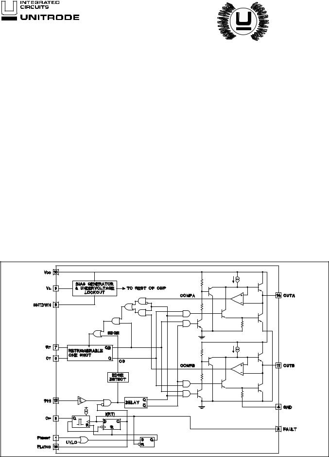
The UC1726 Isolated Drive Transmitter, and its companion chip, the UC1727 Isolated High Side IGBT Driver, provide a unique solution to driving isolated power IGBTs. They are particularly suited to drive the high side devices on a high voltage H-bridge. The UC1726 device transmits the drive logic and drive power, along with transferring and receiving fault information with the isolated gate circuit using a low cost pulse transformer.
This drive system utilizes a duty cycle modulation technique that gives instantaneous response to the drive control transitions, and reliably passes steady state, or DC conditions. High frequency operation, up to 750kHz, allows the cost and size of the coupling transformer to be minimized.
The UC1726 can be powered from a single VCC supply which internally generates a voltage reference for the logic circuitry. It can also be placed into a low power shutdown mode that disables the internal reference. The IC’s logic circuitry can be powered from an external supply, VL, to minimize overall power dissipation. Fault logic monitors the Isolated High Side IGBT Driver UC1727 for faults. Based on user defined timing, the UC1726 distinguishes valid faults, which it responds to by setting the fault latch pin. This also disables the gate drive information until the fault reset pin is toggled to a logic one.
The UC1726 operates over an 8 to 35 volt supply range. The typical VCC voltage will be greater than 28 volts to be compatible with the UC1727. The undervoltage lockout circuitry of the Isolated High Side IGBT Driver UC1727 locks out the drive information during its undervoltage lockout.
BLOCK DIAGRAM
UDG-94004-1 |
7/95 |

ABSOLUTE MAXIMUM RATINGS
Supply Voltage VCC . . . . . . . . . . . . . . . . . . . . . . . . . . . . . 40V Source/Sink Current (Pulsed). . . . . . . . . . . . . . . . . . . . . . 1.5A Source/Sink Current (Continuous) . . . . . . . . . . . . . . . . . . 1.0A Output Voltage (pins 12, 14). . . . . . . . . . −0.3 to (VCC + 0.3)V CF, FRESET, FAULT, SHTDWN,
FLATCH, VL, PHI, RT . . . . . . . . . . . . . . . . . . . . . . . −0.3 to 6.0V CT . . . . . . . . . . . . . . . . . . . . . . . . . . . . . . . . . . . . . . 1.0 to 6.0V Operating Junction Temperature (Note 2) . . . . . . . . . . 150°C Storage Temperature Range . . . . . . . . . . . . . −65°C to 150°C Lead Temperature (Soldering, 10 seconds). . . . . . . . . 300°C
Note 1: All voltages are with respect to GND (Pin 2); all currents are positive into, negative out of part.
UC1726
UC2726
UC3726
RECOMMENDED OPERATING CONDITIONS (Note 3)
Input Voltage. . . . . . . . . . . . . . . . . . . . . . . . . . . . . . . +9 to +35.0V Sink/Source Current (each output) . . . . . . . . . . . . . . . 0 to 750mA Timing Resistor. . . . . . . . . . . . . . . . . . . . . . . . . . . . 2.4k to 200kΩ Timing Capacitor (CT). . . . . . . . . . . . . . . . . . . . . . . 75pF to 2.0nF Timing Capacitor (CF). . . . . . . . . . . . . . . . . . . . . . . 75pF to 3.0nF
Note 2: See Unitrode Integrated Circuits databook for information regarding thermal specifications and limitations of packages.
Note 3: Range over which the device is functional and parameter limits are guaranteed.
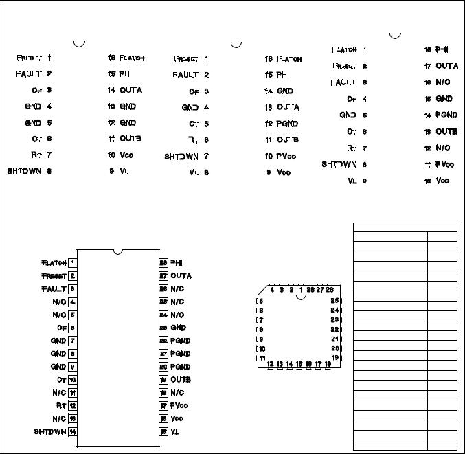
CONNECTION DIAGRAMS
DIL-16 (Top View) |
|
|
|
|
|
|
|
|
|
|
|
|
|
|
|
|
|
|
|
|
|
|
DIL-16 (Top View) |
|
|
|
|
|
|
|
|
|
|
|
|
|
|
|
|
|
|
|
|
|
DIL-18 (Top View) |
|
|
|
|
||||||||||||||||||||||||||||||||||||||||||||||||||||||||||||||||||||||||||||
N Package |
|
|
|
|
|
|
|
|
|
|
|
|
|
|
|
|
|
|
|
|
|
|
SP Package |
|
|
|
|
|
|
|
|
|
|
|
|
|
|
|
|
|
|
|
|
|
J Package |
|
|
|
|
||||||||||||||||||||||||||||||||||||||||||||||||||||||||||||||||||||||||||||
|
|
|
|
|
|
|
|
|
|
|
|
|
|
|
|
|
|
|
|
|
|
|
|
|
|
|
|
|
|
|
|
|
|
|
|
|
|
|
|
|
|
|
|
|
|
|
|
|
|
|
|
|
|
|
|
|
|
|
|
|
|
|
|
|
|
|
|
|
|
|
|
|
|
|
|
|
|
|
|
|
|
|
|
|
|
|
|
|
|
|
|
|
|
|
|
|
|
|
|
|
|
|
|
|
|
|
|
|
|
|
|
|
|
|
|
|
|
|
|
|
|
|
|
|
|
|
|
|
|
|
|
|
|
|
|
|
|
|
|
|
|
|
|
|
|
|
|
|
|
|
|
|
|
|
|
|
|
|
|
|
|
|
|
|
|
|
|
|
|
|
|
|
|
|
|
|
|
|
|
|
|
|
|
|
|
|
|
|
|
|
|
|
|
|
|
|
|
|
|
|
|
|
|
|
|
|
|
|
|
|
|
|
|
|
|
|
|
|
|
|
|
|
|
|
|
|
|
|
|
|
|
|
|
|
|
|
|
|
|
|
|
|
|
|
|
|
|
|
|
|
|
|
|
|
|
|
|
|
|
|
|
|
|
|
|
|
|
|
|
|
|
|
|
|
|
|
|
|
|
|
|
|
|
|
|
|
|
|
|
|
|
|
|
|
|
|
|
|
|
|
|
|
|
|
|
|
|
|
|
|
|
|
|
|
|
|
|
|
|
|
|
|
|
|
|
|
|
|
|
|
|
|
|
|
|
|
|
|
|
|
|
|
|
|
|
|
|
|
|
|
|
|
|
|
|
|
|
|
|
|
|
|
|
|
|
|
|
|
|
|
|
|
|
|
|
|
|
|
|
|
|
|
|
|
|
|
|
|
|
|
|
|
|
|
|
|
|
|
|
|
|
|
|
|
|
|
|
|
|
|
|
|
|
|
|
|
|
|
|
|
|
|
|
|
|
|
|
|
|
|
|
|
|
|
|
|
|
|
|
|
|
|
|
|
|
|
|
|
|
|
|
|
|
|
|
|
|
|
|
|
|
|
|
|
|
|
|
|
|
|
|
|
|
|
|
|
|
|
|
|
|
|
|
|
|
|
|
|
|
|
|
|
|
|
|
|
|
|
|
|
|
|
|
|
|
|
|
|
|
|
|
|
|
|
|
|
|
|
|
|
|
|
|
|
|
|
|
|
|
|
|
|
|
|
|
|
|
|
|
|
|
|
|
|
|
|
|
|
|
|
|
|
|
|
|
|
|
|
|
|
|
|
|
|
|
|
|
|
|
|
|
|
|
|
|
|
|
|
|
|
|
|
|
|
|
|
|
|
|
|
|
|
|
|
|
|
|
|
|
|
|
|
|
|
|
|
|
|
|
|
|
|
|
|
|
|
|
|
|
|
|
|
|
|
|
|
|
|
|
|
|
|
|
|
|
|
|
|
|
|
|
|
|
|
|
|
|
|
|
|
|
|
|
|
|
|
|
|
|
|
|
|
|
|
|
|
|
|
|
|
|
|
|
|
|
|
|
|
|
|
|
|
|
|
|
|
|
|
|
|
|
|
|
|
|
|
|
|
|
|
|
|
|
|
|
|
|
|
|
|
|
|
|
|
|
|
|
|
|
|
|
|
|
|
|
|
|
|
|
|
|
|
|
|
|
|
|
|
|
|
|
|
|
|
|
|
|
|
|
|
|
|
|
|
|
|
|
|
|
|
|
|
|
|
|
|
|
|
|
|
|
|
|
|
|
|
|
|
|
|
|
|
|
|
|
|
|
|
|
|
|
|
|
|
|
|
|
|
|
|
|
|
|
|
|
|
|
|
|
|
|
|
|
|
|
|
|
|
|
|
|
|
|
|
|
|
|
|
|
|
|
|
|
|
|
|
|
|
|
|
|
|
|
|
|
|
|
|
|
|
|
|
|
|
|
|
|
|
|
|
|
|
|
|
|
|
|
|
|
|
|
|
|
|
|
|
|
|
|
|
|
SOIC-28 (Top View) |
PLCC-28 (Top View) |
PACKAGE PIN FUNCTION |
|
DWP Package |
QP Package |
FUNCTION |
PIN |
|
|
GND |
1 |
|
|
CT |
2 |
|
|
N/C |
3-4 |
|
|
RT |
5 |
|
|
SHTDWN |
6 |
|
|
VL |
7 |
|
|
VCC |
8 |
|
|
N/C |
9 |
|
|
PVCC |
10 |
|
|
OUTB |
11 |
|
|
PGND |
12-18 |
|
|
GND |
19 |
|
|
OUTA |
20 |
|
|
PHI |
21 |
|
|
FLATCH |
22 |
|
|
FRESET |
23 |
|
|
FAULT |
24 |
|
|
N/C |
25 |
|
|
CF |
26 |
|
|
N/C |
27 |
|
|
N/C |
28 |
2
 Loading...