


Texas Instruments UC3854BQ, UC3854BN, UC3854BDWTR, UC3854BDW, UC3854AN Datasheet
...
UC1854A/B
UC2854A/B
UC3854A/B
Enhanced High Power Factor Preregulator
FEATURES
∙Controls Boost PWM to Near Unity Power Factor
∙Limits Line Current Distortion To <3%
∙World-Wide Operation Without Switches
∙Accurate Power Limiting
∙Fixed Frequency Average Current Mode Control
∙High Bandwidth (5MHz), Low Offset Current Amplifier
∙Integrated Current and Voltage Amp Output Clamps
∙Multiplier Improvements: Linearity, 500mV VAC Offset (eliminates external resistor), 0-5V Multout Common Mode Range
∙VREF "GOOD" Comparator
∙Faster and Improved Accuracy ENABLE Comparator
∙UVLO Threshold Options (16/10V / 10.5/10V)
∙300μA Startup Supply Current
|
UVLO Turn on |
UVLO Turn off |
UC1854A |
16V |
10V |
UC1854B |
10.5V |
10V |
DESCRIPTION
The UC1854A/B products are pin compatible enhanced versions of the UC1854. Like the UC1854, these products provide all of the functions necessary for active power factor corrected preregulators. The controller achieves near unity power factor by shaping the AC input line current waveform to correspond to the AC input line voltage. To do this the UC1854A/B uses average current mode control. Average current mode control maintains stable, low distortion sinusoidal line current without the need for slope compensation, unlike peak current mode control.
The UC1854A/B products improve upon the UC1854 by offering a wide bandwidth, low offset Current Amplifier, a faster responding and improved accuracy enable comparator, a VREF "good" comparator, UVLO threshold options (16/10V for offline, 10.5/10V for startup from an auxiliary 12V regulator), lower startup supply current, and an enhanced multiply/divide circuit. New features like the amplifier output clamps, improved amplifier current sinking capability, and low offset VAC pin reduce the external component count while improving performance. Improved common mode input range of the Multiplier output/Current Amp input allow the designer greater flexibility in choosing a method for current sensing. Unlike its predecessor, RSET controls only oscillator charging current and has no effect on clamping the maximum multiplier output current. This current is now clamped to a maximum of 2 * IAC at all times which simplifies the design process and provides foldback power limiting during brownout and extreme low line conditions.
A 1% 7.5V reference, fixed frequency oscillator, PWM, Voltage Amplifier with softstart, line voltage feedforward (VRMS squarer), input supply voltage clamp, and over current comparator round out the list of features.
BLOCK DIAGRAM
UDG-93001-1 |
6/98 |
ABSOLUTE MAXIMUM RATINGS
Supply Voltage VCC . . . . . . . . . . . . . . . . . . . . . . . . . . . . . . 22V
GT Drv Current, Continuous . . . . . . . . . . . . . . . . . . . . . . . 0.5A
GT Drv Current, 50% Duty Cycle. . . . . . . . . . . . . . . . . . . . 1.5A
Input Voltage, VSENSE, VRMS . . . . . . . . . . . . . . . . . . . . . . . 11V
Input Voltage, ISENSE, Mult Out . . . . . . . . . . . . . . . . . . . . . 11V
Input Voltage, PKLMT . . . . . . . . . . . . . . . . . . . . . . . . . . . . . 5V
Input Current, RSET, IAC, PKLMT, ENA . . . . . . . . . . . . . . 10mA
Power Dissipation . . . . . . . . . . . . . . . . . . . . . . . . . . . . . . . . 1W
Storage Temperature . . . . . . . . . . . . . . . –65°C to +150°C
Lead Temperature (Soldering, 10 Seconds) . . . . . . . . . +300°C
UC1854A/B
UC2854A/B
UC3854A/B
Note 1: All voltages with respect to Gnd (Pin 1).
Note 2: All currents are positive into the specified terminal. Note 3: ENA imput is internally clamped to approximately 10V. Note 4: Consult Unitrode Integrated Circuits databook for information regarding thermal specifications and limitations of packages.
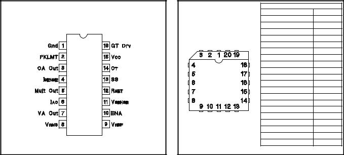
CONNECTION DIAGRAMS
DIL–16 & SOIC-16 |
PLCC-20 & LCC-20 |
PACKAGE PIN FUNCTION |
|
(Top View) |
(Top View) |
FUNCTION |
PIN |
J, N & DW Packages |
Q & L Packages |
N/C |
1 |
|
|
Gnd |
2 |
|
|
PKLMT |
3 |
|
|
CA Out |
4 |
|
|
ISENSE |
5 |
|
|
N/C |
6 |
|
|
Mult Out |
7 |
|
|
IAC |
8 |
|
|
VA Out |
9 |
|
|
VRMS |
10 |
|
|
N/C |
11 |
|
|
VREF |
12 |
|
|
ENA |
13 |
|
|
VSENSE |
14 |
|
|
RSET |
15 |
|
|
N/C |
16 |
|
|
SS |
17 |
|
|
CT |
18 |
|
|
VCC |
19 |
|
|
GT Drv |
20 |
ELECTRICAL CHARACTERISTICS Unless otherwise stated, VCC=18V, RT=8.2k, CT=1.5nF, PKLMT=1V, VRMS=1.5V, |
|||||
|
IAC=100μA, ISENSE=0V, CA Out=3.5V, VA Out=5V, VSENSE=3V, –55oC<TA<125oC |
||||
|
for the UC1854A/B, –40oC<TA<85oC for the UC2854A/B, and 0oC<TA<70oC for the |
||||
|
UC3854A/B, and TA=TJ. |
|
|
|
|
|
|
|
|
|
|
PARAMETER |
TEST CONDITIONS |
MIN |
TYP |
MAX |
UNITS |
OVERALL |
|
|
|
|
|
Supply Current, Off |
CAO, VAO = 0V, VCC = UVLO - 0.3V |
|
250 |
400 |
μA |
Supply Current, On |
|
|
12 |
18 |
mA |
VCC Turn-On Threshold |
UC1854A |
|
16 |
17.5 |
V |
|
UC1854B |
|
10.5 |
11.2 |
V |
VCC Turn-Off Threshold |
UC1854A / B |
9 |
10 |
|
V |
VCC Clamp |
I(VCC) = ICC(on) + 5mA |
18 |
20 |
22 |
V |
|
|
|
|
|
|
VOLTAGE AMPLIFIER |
|
|
|
|
|
Input Voltage |
|
2.9 |
3.0 |
3.1 |
V |
VSENSE Bias Current |
|
–500 |
–25 |
500 |
nA |
Open Loop Gain |
VOUT = 2 to 5V |
70 |
100 |
|
dB |
VOUT High |
ILOAD = –500μA |
|
6 |
|
V |
VOUT Low |
ILOAD = 500μA |
|
0.3 |
0.5 |
V |
Output Short Circuit Current |
VOUT = 0V |
|
1.5 |
3.5 |
mA |
|
|
|
|
|
|
Gain Bandwidth Product |
Fin = 100kHz, 10mV p-p, (Note 1) |
|
1 |
|
mHz |
2

ELECTRICAL
CHARACTERISTICS (cont.)
UC1854A/B
UC2854A/B
UC3854A/B
Unless otherwise stated, VCC=18V, RT=8.2k, CT=1.5nF, PKLMT=1V, VRMS=1.5V,
IAC=100μA, ISENSE=0V, CA Out=3.5V, VA Out=5V, VSENSE=3V, –55oC<TA<125oC for the UC1854A/B, –40oC<TA<85oC for the UC2854A/B, and 0oC<TA<70oC for the UC3854A/B, and TA=TJ.
PARAMETER |
TEST CONDITIONS |
|
MIN |
TYP |
MAX |
UNITS |
CURRENT AMPLIFIER |
|
|
|
|
|
|
Input Offset Voltage |
VCM = 0V |
TA = +25°C |
−4 |
|
0 |
mV |
|
|
OverTemp |
–5.5 |
|
0 |
mV |
Input Bias Current(sense) |
VCM = 0V |
|
–500 |
|
500 |
nA |
Open Loop Gain |
VCM = 0V, VOUT = 2 to 6V |
|
80 |
110 |
|
dB |
VOUT High |
ILOAD = –500μA |
|
|
8 |
|
V |
VOUT Low |
ILOAD = 500μA |
|
|
0.3 |
0.5 |
V |
Output Short Circuit Current |
VOUT = 0V |
|
|
1.5 |
3.5 |
mA |
Common Mode Range |
|
|
–0.3 |
|
5 |
V |
Gain Bandwidth Product |
Fin = 100kHz, 10mV p-p, (Note 1) |
|
3 |
5 |
|
mHz |
REFERENCE |
|
|
|
|
|
|
Output Voltage |
IREF = 0mA, TA = 25oC |
|
7.4 |
7.5 |
7.6 |
V |
|
IREF = 0mA |
|
7.35 |
7.5 |
7.65 |
V |
Load Regulation |
IREF = 1 to 10mA |
|
0 |
8 |
20 |
mV |
Line Regulation |
VCC = 12 to 18V |
|
0 |
14 |
25 |
mV |
Short Circuit Current |
VREF = 0V |
|
25 |
35 |
60 |
mA |
OSCILLATOR |
|
|
|
|
|
|
Initial Accuracy |
TA = 25oC |
|
85 |
100 |
115 |
kHz |
Voltage Stability |
VCC = 12 to 18V |
|
|
1 |
|
% |
Total Variation |
Line, Temp |
|
80 |
|
120 |
kHz |
Ramp Amplitude (p-p) |
|
|
4.9 |
|
5.9 |
V |
Ramp Valley Voltage |
|
|
0.8 |
|
1.3 |
V |
ENABLE / SOFTSTART / CURRENT LIMIT |
|
|
|
|
|
|
Enable Threshold |
|
|
2.35 |
2.55 |
2.8 |
V |
Enable Hysteresis |
VFAULT = 2.5V |
|
|
500 |
600 |
mV |
Enable Input Bias Current |
VENABLE = 0V |
|
|
–2 |
–5 |
μA |
Propagation Delay to Disable |
Enable Overdrive = –100mV,(Note 1) |
|
300 |
|
ns |
|
SS Charge Current |
VSOFTSTART = 2.5V |
|
10 |
14 |
24 |
|
PKLMT Offset Voltage |
|
|
–15 |
|
15 |
mV |
|
|
|
|
|
|
|
PKLMT Input Current |
VPKLMT = –0.1V |
|
–200 |
–100 |
|
μA |
PKLMT Propagation Delay |
(Note 1) |
|
|
150 |
|
ns |
MULTIPLIER |
|
|
|
|
|
|
Output Current - IAC Limited |
IAC=100μA, VRMS = 1V, RSET = 10k |
–220 |
–200 |
–170 |
μA |
|
Output Current - Zero |
IAC=0μA, RSET = 10k |
|
–2.0 |
–0.2 |
2.0 |
μA |
Output Current - Power Limited |
VRMS = 1.5V, Va = 6V |
|
–230 |
–200 |
–170 |
μA |
Output Current |
VRMS = 1.5V, Va = 2V |
|
|
–22 |
|
μA |
|
|
|
|
|
|
|
|
VRMS = 1.5V, Va = 5V |
|
|
–156 |
|
μA |
|
VRMS = 5V, Va = 2V |
|
|
–2 |
|
μA |
|
VRMS = 5V, Va = 5V |
|
|
–14 |
|
μA |
Gain Constant |
(Note 2) VRMS = 1.5V, TJ = 25°C, Va = 6V |
–1.1 |
–1.0 |
–0.9 |
A/A |
|
|
|
|
|
|
|
|
Note 1: Guaranteed by design, not 100% tested in production.
IAC × (Va − 1.5V)
VRMS 2 × IMO
3
 Loading...