


Texas Instruments UCC3581Q, UCC3581N, UCC3581DTR, UCC3581D, UCC2581Q Datasheet
...
UCC1581
UCC2581
UCC3581
Micropower Voltage Mode PWM
FEATURES |
BLOCK DIAGRAM |
∙ Low 85μA Startup Current |
|
∙ Low 300μA Operating Current |
|
∙ Automatically Disabled |
|
Startup Preregulator |
|
∙ Programmable Minimum Duty |
|
Cycle with Cycle Skipping |
|
∙ Programmable Maximum |
|
Duty Cycle |
|
∙ Output Current 1A Peak |
|
Source and Sink |
|
∙ Programmable Soft Start |
|
∙ Programmable Oscillator |
|
Frequency |
|
∙ External Oscillator |
|
Synchronization Capability |
|
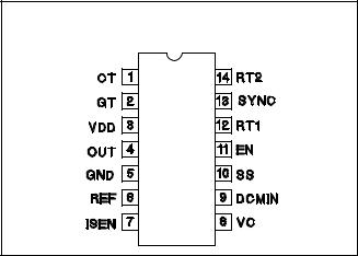
Note: Pin Connection shown for 14-pin Package |
UDG-95011-1 |
|
DESCRIPTION
The UCC3581 voltage mode pulse width modulator is designed to control low power isolated DC - DC converters in applications such as Subscriber Line Power (ISDN I.430). Primarily used for single switch forward and flyback converters, the UCC3581 features BiCMOS circuitry for low startup and operating current, while maintaining the ability to drive power MOSFETs at frequencies up to 100kHz. The UCC3581 oscillator allows the flexibility to program both the frequency and the maximum duty cycle with two resistors and a capacitor. A TTL level input is also provided to allow synchronization to an external frequency source.
The UCC3581 includes programmable soft start circuitry, overcurrent detection, a 7.5V linear preregulator to control chip VDD during startup, and an on-board 4.0V logic supply.
The UCC3581 provides functions to maximize light load efficiency that are not normally found in PWM controllers.
A linear preregulator driver in conjunction with an external depletion mode N-MOSFET provides initial controller power. Once the bootstrap supply is functional, the preregulator is shut down to conserve power. During light load, power is saved by providing a programmable minimum duty cycle clamp. When a duty cycle below the minimum is called for, the modulator skips cycles to provide the correct average duty cycle required for output regulation. This effectively reduces the switching frequency, saving significant gate drive and power stage losses.
The UCC3581 is available in 14-pin plastic and ceramic dual-in-line packages and in a 14-pin narrow body small outline IC package (SOIC). The UCC1581 is specified for operation from −55°C to +125°C, the UCC2581 is specified for operation from −40°C to +85°C, and the UCC3581 is specified for operation from 0°C to +70°C.
SLUS295 - MARCH 1999
ABSOLUTE MAXIMUM RATINGS
Supply Voltage (IDD ≤ 10mA). . . . . . . . . . . . . . . . . . . . . . . . 15V Supply Current . . . . . . . . . . . . . . . . . . . . . . . . . . . . . . . . . 30mA
VREF Current. . . . . . . . . . . . . . . . . . . . . . . . . . . . . . . . . . –10mA OUT Current . . . . . . . . . . . . . . . . . . . . . . . . . . . . . . . . . . . . ± 1A
Analog Inputs
EN . . . . . . . . . . . . . . . . . . . . . . . . . . . . –0.3V to (VDD + 0.3V)
VC, ISEN, SYNC, DCMIN. . . . . . . . . . –0.3V to (VREF + 0.3V) Power Dissipation at TD = 25°C
(N, J, Q, L Package) . . . . . . . . . . . . . . . . . . . . . . . . . . . . . 1W (D Package) . . . . . . . . . . . . . . . . . . . . . . . . . . . . . . . . . 0.65W Storage Temperature . . . . . . . . . . . . . . . . . . . –65°C to +150°C Junction Temperature . . . . . . . . . . . . . . . . . . . –55C to +150°C Lead Temperature (Soldering, 10 sec.) . . . . . . . . . . . . . +300°C
Unless otherwise specified, all voltages are with respect to Ground. Currents positive into, negative out of the specified terminal. Consult Packaging Section of Databook for thermal limitations and considerations of packages.
UCC1581
UCC2581
UCC3581
CONNECTION DIAGRAMS
DIL-14, SOIC-14 (Top View)
N or J, D Packages
ORDERING INFORMATION
|
TEMPERATURE RANGE |
PACKAGE |
UCC1581J |
–55°C to +125°C |
CDIP |
UCC2581D |
–40°C to +85°C |
SOIC |
UCC2581N |
–40°C to +85°C |
PDIP |
UCC3581D |
0°C to +70°C |
SOIC |
UCC3581N |
0°C to +70°C |
PDIP |
ELECTRICAL CHARACTERISTICS: Unless otherwise stated, these specifications apply for VDD = 10V, 0.1μF capacitor from VDD to GND, 1.0μF capacitor from REF to GND, RT1 = 680kΩ, RT2 = 12kΩ, CT = 750pF and TA = TJ.
PARAMETER |
TEST CONDITIONS |
MIN |
TYP |
MAX |
UNITS |
Reference Section |
|
|
|
|
|
Output Voltage |
I = –0.2mA |
3.94 |
4.0 |
4.06 |
V |
Load Regulation |
–5.0mA < I < –0.2mA |
|
10 |
30 |
mV |
Undervoltage Lockout Section |
|
|
|
|
|
Start Threshold |
|
6.7 |
7.3 |
7.9 |
V |
Minimum Operating Voltage After Start |
|
6.2 |
6.8 |
7.4 |
V |
Hysteresis |
|
0.2 |
0.5 |
0.8 |
V |
Linear Preregulator Section |
|
|
|
|
|
Regulated VDD Voltage |
|
7.0 |
7.5 |
8.0 |
V |
Regulated VDD to UVLO Delta |
|
100 |
230 |
600 |
mV |
VDD Override Threshold |
|
|
|
8.2 |
V |
Oscillator Section |
|
|
|
|
|
Frequency |
25°C |
18 |
19.5 |
21 |
kHz |
Temperature Stability |
(Note 1) |
|
3.0 |
|
% |
CT Peak Voltage |
(Note 1) |
|
2.5 |
|
V |
CT Valley Voltage |
(Note 1) |
|
1.0 |
|
V |
SYNC VIH |
|
1.9 |
2.1 |
2.3 |
V |
SYNC VIL |
(Note 1) |
|
1.8 |
|
V |
PWM SECTION |
|
|
|
|
|
Maximum Duty Cycle |
|
80 |
83 |
86 |
% |
Minimum Duty Cycle |
(VC < 1.0V) DCMIN = 0V |
|
|
0 |
% |
|
(VC > 1.0V at start of cycle) DCMIN = 1.18V |
8 |
10.5 |
13 |
% |
Input Bias Current |
(DCMIN), (Note 1) |
–150 |
20 |
150 |
nA |
|
(VC), (Note 1) |
–150 |
20 |
150 |
nA |
2

UCC1581
UCC2581
UCC3581
ELECTRICAL CHARACTERISTICS: Unless otherwise stated, these specifications apply for VDD = 10V, 0.1μF capacitor from VDD to GND, 1.0μF capacitor from REF to GND, RT1 = 680kΩ, RT2 = 12kΩ, CT = 750pF and TA = TJ.
PARAMETER |
TEST CONDITIONS |
MIN |
TYP |
MAX |
UNITS |
Current Sense Section |
|
|
|
|
|
Input Bias Current |
|
–150 |
20 |
150 |
nA |
Overcurrent Threshold |
|
0.4 |
0.5 |
0.6 |
V |
Output Section |
|
|
|
|
|
OUT Low Level |
I = 100mA |
|
0.6 |
1.2 |
V |
OUT High Level |
I = –100mA, VDD – OUT |
|
0.6 |
1.2 |
V |
Rise/Fall Time |
(Note 1) |
|
20 |
100 |
ns |
Soft start Section |
|
|
|
|
|
Soft start Current |
SS = 2V |
–9 |
–11.5 |
–14 |
μA |
Chip Enable Section |
|
|
|
|
|
VIH |
|
1.9 |
2.0 |
2.1 |
V |
VIL |
|
1.7 |
1.8 |
1.9 |
V |
Hysteresis |
|
180 |
230 |
280 |
mV |
Source Current |
|
5 |
10 |
15 |
μA |
Overall Section |
|
|
|
|
|
Start-Up Current |
VDD < Start Threshold |
|
85 |
130 |
μA |
Operating Supply Current |
VC = 0V |
|
300 |
600 |
μA |
VDD Zener Shunt Voltage |
IDD = 10mA |
13.5 |
15 |
16.5 |
V |
IDD Stand-by Shunt Voltage |
EN = 0V |
|
100 |
150 |
μA |
Note 1: Guaranteed by design. Not 100% tested in production
PIN DESCRIPTIONS
CT: Oscillator timing capacitor pin. Minimum value is 100pF.
DCMIN: Input for programming minimum duty cycle where pulse skipping begins. This pin can be grounded to disable minimum duty cycle feature and pulse skipping.
EN: Enable input. This pin has an internal 10mA pull-up. A logic low input inhibits the PWM output and causes the soft start capacitor to be discharged.
GND: Circuit ground.
GT: Pin for controlling the gate of an external depletion mode N-MOSFET for the startup supply. The external N-MOSFET regulates VDD to 7.5V until the bootstrap supply comes up, then GT goes low.
ISEN: Input for overcurrent comparator. This function can be used for pulse-by-pulse current limiting. The threshold is 0.5V nominal.
OUT: Gate drive output to external N-MOSFET.
REF: 4.0V reference output. A minimum value bypass capacitor of 1.0mF is required for stability.
RT1: Resistor pin to program oscillator charging current.
æ 2.0V ö The oscillator charging current is 9.2 · çè RT1 ÷ø .
See Application Diagram Fig. 1.
æ 2.0V ö The current into this pin is çè RT1 ÷ø .
The value of RT1 should be between 220k and 1MW.
RT2: Resistor pin to program oscillator discharge time. The minimum value of RT2 is 10kW. See Application Diagram Fig. 1.
SS: Soft start capacitor pin. The charging current out of SS is 3.75X the current in RT1.
SYNC: Oscillator synchronization pin. Rising edge triggered CMOS/TTL compatible input with a 2.1V threshold. SYNC should be grounded if not used. The minimum pulse width of the SYNC signal is 100ns.
VC: Control voltage input to PWM comparator. The nominal control range of VC is 1.0V to 2.5V.
VDD: Chip input power with an 15V internal clamp. VDD is regulated by startup FET to 7.5V until the bootstrap voltage comes up. VDD should be bypassed at the chip with a 0.1mF minimum capacitor.
3
 Loading...