


Texas Instruments UC3879N, UC3879J, UC3879DWTR, UC3879DW, UC2879N Datasheet
...
UC1879
UC2879
UC3879
Phase Shift Resonant Controller
FEATURES
∙Programmable Output Turn On Delay; Zero Delay Available
∙Compatible with Voltage Mode or Current Mode Topologies
∙Practical Operation at Switching Frequencies to 300kHz
∙Four 100mA Totem Pole Outputs
∙10MHz Error Amplifier
∙Pin Programmable Undervoltage Lockout
∙Low Startup Current - 150μA
∙Soft Start Control
∙Outputs Active Low During UVLO
BLOCK DIAGRAM
DESCRIPTION
The UC3879 controls a bridge power stage by phase shifting the switching of one half-bridge with respect to the other. This allows constant frequency pulse width modulation in combination with resonant, zero-voltage switching for high efficiency performance. The UC3879 can be configured to provide control in either voltage mode or current mode operation, with overcurrent shutdown for fast fault protection.
Independently programmable time delays provide dead-time at the turn-on of each output stage, allowing time for each resonant switching interval.
With the oscillator capable of operating in excess of 600kHz, overall output switching frequencies to 300kHz are practical. In addition to the standard free running mode, with the CLKSYNC pin, the user may configure the UC3879 to accept an external clock synchronization signal. Alternatively, up to three units can be locked together with the operational frequency determined by the fastest device.
Protective features include an undervoltage lockout and overcurrent protection. Additional features include a 10MHz error amplifier, a 5V precision reference, and soft start. The UC3879 is available in 20 pin N, J, DW, and Q and 28 pin L packages.
UDG-94070-1 |
6/98 |
ABSOLUTE MAXIMUM RATINGS
Supply Voltage (VC, VIN) . . . . . . . . . . . . . . . . . . . . . . . . . . 20V Output Current, Source or Sink, DC . . . . . . . . . . . . . . . . . 20mA Analog I/0s
(Pins 1, 2, 3, 4, 5, 6, 14, 15, 17, 18, 19) . . . . . . −0.3 to 5.3V (Pin 16) . . . . . . . . . . . . . . . . . . . . . . . . . . . . . . . −.03V to VIN Storage Temperature Range . . . . . . . . . . . . . −65°C to +150°C Junction Temperature . . . . . . . . . . . . . . . . . . . −55°C to +150°C Lead Temperature (Soldering, 10 sec.) . . . . . . . . . . . . +300°C
Notes: Pin references are to 20 pin DIL and SOIC packages. All voltages are with respect to ground unless otherwise stated. Currents are positive into, negative out of the specified terminal. Consult Packaging Section of Databook for thermal limitations and considerations of packages.
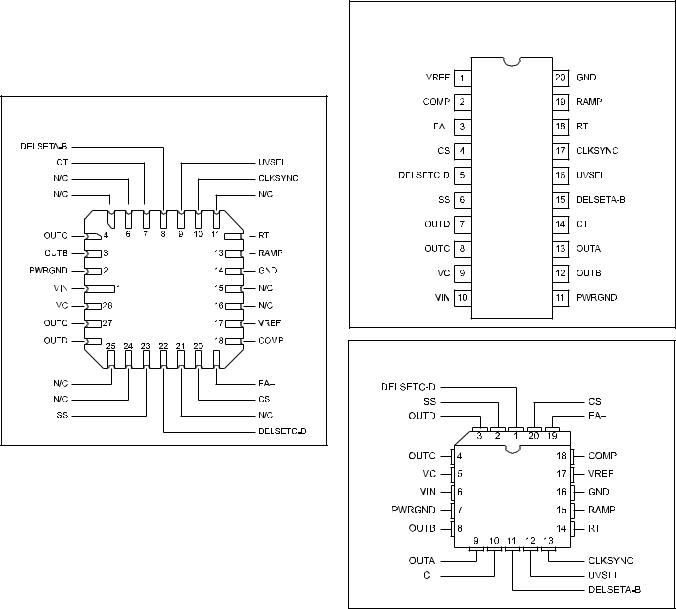
CLCC-28 (Top View)
L Package
UC1879
UC2879
UC3879
Table I. Product Selection Guide
|
TEMPERATURE |
AVAILABLE |
|
RANGE |
PACKAGES |
UCC1879 |
– 55°C to +125°C |
J, L |
UCC2879 |
– 40°C to +85°C |
N, DW, Q, J, L |
UCC3879 |
0°C to +70°C |
N, DW, Q |
CONNECTION DIAGRAMS
DIL-20, SOIC-20 (Top View)
J or N Package, DW Package
PLCC-20 (Top View)
Q Package
2
UC1879
UC2879
UC3879
ELECTRICAL CHARACTERISTICS Unless specified; VC = VIN = VUVSEL =12V, CT = 470pF, RT = 9.53k, RDELSETA-B = RDELSEC-D = 4.8k, CDELSETA-B = CDELSETC-D = 0.01μF, TA = TJ.
PARAMETER |
TEST CONDITIONS |
MIN |
TYP |
MAX |
UNITS |
Undervoltage Lockout |
|
|
|
|
|
Start Threshold |
VUVSEL = VIN |
9 |
10.75 |
12.5 |
V |
|
VUVSEL = Open |
12.5 |
15.25 |
16.5 |
V |
UVLO Hysteresis |
VUVSEL = VIN |
1.15 |
1.75 |
2.15 |
V |
|
VUVSEL = Open |
5.2 |
6 |
7.4 |
V |
Input Bias, UVSEL Pin |
VUVSEL = VIN = 8V |
|
30 |
|
μA |
Supply Current |
|
|
|
|
|
IVIN Startup |
VIN = VUVSEL = 8V, VC = 18V, IDELSETA-B = |
|
150 |
600 |
μA |
|
IDELSETC-D = 0 |
|
|
|
|
IVC Startup |
VIN = VUVSEL = 8V, VC = 18V, IDELSETA-B = |
|
10 |
100 |
μA |
|
IDELSETC-D = 0 |
|
|
|
|
IVIN Operating |
UC3879, UC2879 |
|
23 |
33 |
mA |
|
UC1879 |
|
23 |
36 |
mA |
IVC Operating |
|
|
4 |
8 |
mA |
Voltage Reference |
|
|
|
|
|
Output Voltage |
TJ = +25°C |
4.92 |
5 |
5.08 |
V |
Line Regulation |
11V < VIN < 18V |
|
1 |
10 |
mV |
Load Regulation |
IVREF = –10mA |
|
5 |
20 |
mV |
Total Variation |
Line, Load, Temperature |
4.875 |
|
5.125 |
V |
Short Circuit Current |
VREF = 0V, TJ = 25°C |
|
–60 |
–15 |
mA |
Error Amplifier |
|
|
|
|
|
Error Amplifier Input Voltage |
|
2.4 |
2.5 |
2.6 |
V |
Input Bias Current |
|
|
0.6 |
3 |
μA |
AVOL |
1V < VCOMP < 4V |
60 |
90 |
|
dB |
PSRR |
11V < VIN < 18V |
85 |
100 |
|
dB |
Output Sink Current |
VCOMP = 1V |
1 |
2.5 |
|
mA |
Output Source Current |
VCOMP = 4V |
|
−1.3 |
−0.5 |
mA |
Output Voltage High |
ICOMP = –0.5mA |
4 |
4.7 |
5 |
V |
Output Voltage Low |
ICOMP = 1mA |
0 |
0.5 |
1 |
V |
Slew Rate |
TA = +25°C |
6 |
11 |
|
V/ μs |
PWM Comparator |
|
|
|
|
|
RAMP Offset Voltage |
TJ = 25°C, Note 3 |
1.1 |
1.25 |
1.4 |
V |
PWM Phase Shift, |
VCOMP > VRAMPpeak + VRAMPoffset |
98 |
99.7 |
102 |
% |
TDELSETA-B, TDELSETC-D = 0, Note 1 |
VCOMP < Zero Phase Shift Voltage |
0 |
0.3 |
2 |
% |
Output Skew, |
VCOMP > VRAMPpeak + VRAMPoffset |
|
10 |
|
ns |
TDELSETA-B, TDELSETC-D = 0, Note 1 |
VCOMP < Zero Phase Shift Voltage |
|
10 |
|
ns |
Ramp to Output Delay, TDELSETA-B = 0, |
UC3879, UC2879 |
|
115 |
250 |
ns |
TDELSETC-D = 0 |
UC1879 |
|
115 |
300 |
ns |
Oscillator |
|
|
|
|
|
Initial Accuracy |
TA = 25°C |
180 |
200 |
220 |
kHz |
Voltage Stability |
11V < VIN < 18V |
|
1 |
2 |
% |
Total Variation |
Line, Temperature |
160 |
200 |
240 |
kHz |
CLKSYNC Threshold |
|
2.3 |
2.5 |
2.7 |
V |
Clock Out High |
|
2.8 |
4 |
|
V |
Clock Out Low |
|
0.5 |
1 |
1.5 |
V |
Clock Out Pulse Width |
|
|
400 |
600 |
ns |
Ramp Valley Voltage |
|
|
0.2 |
0.4 |
V |
3
 Loading...