


Texas Instruments UCC3889D, UCC3889N, UCC3889DTR, UCC2889N, UCC2889DTR Datasheet
...
UCC1889
UCC2889
UCC3889
Off-line Power Supply Controller
FEATURES
∙Transformerless Off-line Applications
∙Ideal Primary-side Bias Supply
∙Efficient BiCMOS Design
∙Wide Input Range
∙Fixed or Adjustable Low Voltage Output
∙Uses Low Cost SMD Inductors
∙Short Circuit Protected
∙Optional Isolation Capability
TYPICAL APPLICATION
DESCRIPTION
The UCC1889 controller is optimized for use as an off-line, low power, low voltage, regulated bias supply. The unique circuit topology utilized in this device can be visualized as two cascaded flyback converters, each operating in the discontinuous mode, and both driven from a single external power switch. The significant benefit of this approach is the ability to achieve voltage conversion ratios of 400V to 12V with no transformer and low internal losses.
The control algorithm utilized by the UCC1889 is to force the switch on time to be inversely proportional to the input line voltage while the switch off time is made inversely proportional to the output voltage. This action is automatically controlled by an internal feedback loop and reference. The cascaded configuration allows a voltage conversion from 400V to 12V to be achieved with a switch duty cycle greater than 10%. This topology also offers inherent short circuit protection since as the output voltage falls to zero, the switch off time approaches infinity.
The output voltage can be easily set to 12V or 18V. Moreover, it can be programmed for other output voltages less than 18V with a few additional components. An isolated version can be achieved with this topology as described further in Unitrode Application Note U-149.
OPERATION
With reference to the application diagram below, when input voltage is first applied, the RON current into TON is directed to VCC where it charges the external capacitor, C3, connected to VCC. As voltage builds on VCC, an internal undervoltage lockout holds the circuit off and the output at DRIVE low until VCC reaches 8.4V. At this time, DRIVE goes high turning on the power switch, Q1, and redirecting the current into TON to the timing capacitor, CT. CT charges to a fixed threshold with a current ICHG=0.8 ∙ (VIN - 4.5V)/RON. Since DRIVE will only be high for as long as CT charges, the power switch on time will be inversely proportional to line voltage. This provides a constant line voltage-switch on time product.
Note: This device incorporates patented technology used under license from Lambda Electronics, Inc.
UDG-93060-1
2/95
OPERATION (cont.)
At the end of the on time, Q1 is turned off and the RON current into TON is again diverted to VCC. Thus the current through RON, which charges CT during the on time, contributes to supplying control power during the off time.
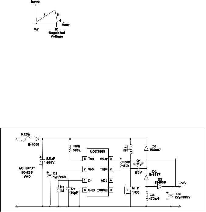
The power switch off time is controlled by the discharge of CT which, in turn, is programmed by the regulated output voltage. The relationship between CT discharge current, IDCHG, and output voltage is illustrated as follows:
1.When VOUT = 0, the off time is infinite. This feature provides inherent short circuit protection. However, to ensure output voltage startup when the output is not a short, a high value resistor, RS, is placed in parallel with CT to establish a minimum switching frequency.
2.As VOUT rises above approximately 0.7V to its regulated value, IDCHG is defined by ROFF, and therefore is equal to:
UCC1889
UCC2889
UCC3889
IDCHG = (VOUT - 0.7V) / ROFF
As VOUT increases, IDCHG increases resulting in the reduction of off time. The frequency of operation increases and VOUT rises quickly to its regulated value.
3.In this region, a transconductance amplifier reduces IDCHG in order to maintain VOUT in regulation.
4.If VOUT should rise above its regulation range, IDCHG falls to zero and the circuit returns to the minimum frequency established by RS and CT.
The range of switching frequencies is established by RON, ROFF, RS, and CT as follows:
Frequency = 1/(TON + TOFF)
TON = RON ∙ CT ∙ 4.6 V/(VIN - 4.5V)
TOFF (max) = 1.4 ∙ RS ∙ CT
Regions 1 and 4
TOFF = ROFF ∙ CT ∙ 3.7V /(VOUT - 0.7V) Region 2, excluding the effects of RS which have a minimal impact on TOFF.
The above equations assume that VCC equals 9V. The voltage at TON increases from approximately 2.5V to 6.5V while CT is charging. To take this into account, VIN is adjusted by 4.5V in the calculation of TON. The voltage at TOFF is approximately 0.7V.
DESIGN EXAMPLE
The UCC3889 regulates a 12 volt, 1 Watt nonisolated DC output from AC inputs between 80 and 265 volts. In this example, the IC is programmed to deliver a maximum on time gate drive pulse width of 2.4 microseconds which occurs at 80 VAC. The corresponding switching frequency is approximately 100kHz at low line, and overall efficiency is approximately 50%. Additional design information is available in Unitrode Application Note U-149.
UDG-93062-3 |
2 |

ABSOLUTE MAXIMUM RATINGS
ICC . . . . . . . . . . . . . . . . . . . . . . . . . . . . . . . . . . . . . . . . . . . . 5mA Current into TON Pin . . . . . . . . . . . . . . . . . . . . . . . . . . . . . 1.5mA Voltage on VOUT Pin. . . . . . . . . . . . . . . . . . . . . . . . . . . . . . . 20V Current into TOFF Pin . . . . . . . . . . . . . . . . . . . . . . . . . . . . 250μA Storage Temperature . . . . . . . . . . . . . . . . . . . . -65°C to +150°C
Note: Unless otherwise indicated, voltages are referenced to ground and currents are positive into, negative out of, the specified terminals.
UCC1889
UCC2889
UCC3889
CONNECTION DIAGRAM
DIL-8, SOIC-8 (Top View)
N or J, D Package
ELECTRICAL CHARACTERISTICS Unless otherwise stated, these specifications hold for TA = 0°C to 70°C for the UCC3889, -40°C to +85°C for the UCC2889, and -55°C to +125°C for the UCC1889.
No load at DRIVE pin (CLOAD=0).
PARAMETER |
TEST CONDITIONS |
MIN |
TYP |
MAX |
UNITS |
General |
|
|
|
|
|
VCC Zener Voltage |
ICC < 1.5mA |
8.6 |
9.0 |
9.3 |
V |
Startup Current |
VOUT = 0 |
|
150 |
250 |
μA |
Operating Current I(VOUT) |
VOUT = 11V, F = 150kHz |
|
1.2 |
2.5 |
mA |
Under-Voltage-Lockout |
|
|
|
|
|
Start Threshold |
VOUT = 0 |
8.0 |
8.4 |
8.8 |
V |
Minimum Operating Voltage after Start |
VOUT = 0 |
6.0 |
6.3 |
6.6 |
V |
Hysteresis |
VOUT = 0 |
1.8 |
|
|
V |
Oscillator |
|
|
|
|
|
Amplitude |
VCC = 9V |
3.5 |
3.7 |
3.9 |
V |
CT to DRIVE high Propagation Delay |
Overdrive = 0.2V |
|
100 |
200 |
ns |
CT to DRIVE low Propagation Delay |
Overdrive = 0.2V |
|
50 |
100 |
ns |
Driver |
|
|
|
|
|
VOL |
I = 20mA, VCC = 9V |
|
0.15 |
0.4 |
V |
|
I = 100mA, VCC = 9V |
|
0.7 |
1.8 |
V |
VOH |
I = −20mA, VCC = 9V |
8.5 |
8.8 |
|
V |
|
I = −100mA, VCC = 9V |
6.1 |
7.8 |
|
V |
Rise Time |
CLOAD = 1nF |
|
35 |
70 |
ns |
Fall Time |
CLOAD = 1nF |
|
30 |
60 |
ns |
Line Voltage Detection |
|
|
|
|
|
Charge Coefficient: ICHG / I(TON) |
VCT = 3V, DRIVE = High, I(TON) = 1mA |
0.73 |
0.79 |
0.85 |
|
Minimum Line Voltage for Fault |
RON = 330k |
60 |
80 |
100 |
V |
Minimum Current I(TON) for Fault |
RON = 330k |
|
220 |
|
μA |
On Time During Fault |
CT = 150pF, VLINE = Min − 1V |
|
2 |
|
μs |
Oscillator Restart Delay after Fault |
|
|
0.5 |
|
ms |
VOUT Error Amp |
|
|
|
|
|
VOUT Regulated 12V (ADJ Open) |
VCC = 9V, IDCHG = I(TOFF)/2 |
11.2 |
11.9 |
12.8 |
V |
VOUT Regulated 18V (ADJ = 0V) |
VCC = 9V, IDCHG = I(TOFF)/2 |
16.5 |
17.5 |
19.5 |
V |
Discharge Ratio: IDCHG / I(TOFF) |
I(TOFF) = 50μA |
0.95 |
1.01 |
1.07 |
|
Voltage at TOFF |
I(TOFF) = 50μA |
0.6 |
0.95 |
1.3 |
V |
Regulation gm (Note 1) |
Max IDCHG = 50μA |
|
1.0 |
|
mA/V |
|
Max IDCHG = 125μA |
0.8 |
1.7 |
2.9 |
mA/V |
IDCHG
when VOUT is in regulation. The two points used to calculate gm are for
VOUT
IDCHG at 65% and 35% of its maximum value.
3
 Loading...