Texas Instruments UCC3752N, UCC3752DTR, UCC3752D, UCC2752N, UCC2752DTR Datasheet
...
Resonant Ring Generator Controller
UCC2752
UCC3752
PRELIMINARY
FEATURES
•Novel Topology for Low-Cost, Efficient Generation of Ring Voltage
•Suitable for Multi-Line Operation
•Selectable 20, 25 and 50 Hz Ring Frequency
•Secondary (AC) Current Limiting Generates an Off-Hook Detect Signal
•Primary Current Limiting to Turn Power Stage Off Under Fault Conditions
•Operates from a Single 12V Supply
DESCRIPTION
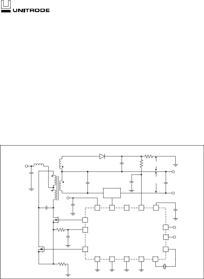
The UCC3752 controller is designed for driving a power stage that generates low frequency, high voltage sinusoidal signals for telephone ringing applications. The controller and the power stage are most suitable for up to 5 line applications where low cost, high efficiency and minimum parts count are critical. A semi-regulated DC voltage is added as an offset to the ringing signal. The ring generator operation is non-isolated and open loop.
The UCC3752 directly drives primary side switches used to implement a push-pull resonant converter topology and transformer coupled sampling switches located on the secondary of the converter. For normal ring signal generation, the primary switching frequency and secondary sampling frequency are precisely offset from each other by the ringing frequency to produce a high voltage low frequency alias signal at the output. The off-hook condition is detected by sensing the AC current and when AC limit is exceeded, a flag is generated on the OFFHOOK pin.
The drive signal frequencies are derived from a high frequency (3579545 Hz) crystal. The primary switching frequency is 89.489 kHz and the sampling frequency is 20, 25 or 50 Hz less depending on the status of frequency select pins FS0 and FS1.
The circuits described in this datasheet are covered under US Patent #5,663,878 and other patents pending.
TYPICAL APPLICATION |
|
|
|
|
|
|
|
|
|
|
|
|
D1 |
|
RSENSE |
|
|
|
|
|
|
|
|
|
||
LIN |
T1 |
|
|
|
CDC |
|
DC SIGNAL |
|
VIN |
|
|
|
|
|
|||
|
|
|
|
|
|
|
|
|
12V |
|
|
|
|
|
|
|
V1 |
|
|
|
|
|
|
|
|
|
LR |
|
|
CR2 |
|
|
|
AC SIGNAL |
CF |
|
|
|
|
|
|
|
||
|
|
|
|
SAMPLING |
|
|
|
VOUT |
LR |
|
|
|
CIRCUIT |
|
|
|
|
|
12V |
|
|
|
|
|
|
|
|
|
|
|
|
|
|
|
|
|
N:1 |
CBYP1 |
|
|
|
|
|
|
|
|
9 |
12 |
2 |
6 |
4 |
|
|
|
|
|
CBYP2 |
|||||
CR1 |
|
|
VS12 |
DRVS |
N/C |
OHD |
VDD |
|
|
|
|
||||||
Q1 |
|
11 |
DRV1 |
|
|
|
|
|
|
|
5 |
DCLIM |
|
UCC3752 |
|
ENABLE |
10 |
|
|
|
|
|
|
|||
|
|
|
|
|
|
|
OFFHOOK |
1 |
Q2 |
|
13 |
DRV2 |
|
|
|
XTAL2 |
15 |
|
|
|
GND |
PGND |
FS0 |
FS1 |
XTAL1 |
|
|
|
|
3 |
14 |
7 |
8 |
16 |
|
|
|
|
|
|
|
|
3.579545MHz |
|
UDG-98058
SLUS269 - JULY 1999

ABSOLUTE MAXIMUM RATINGS
Input Supply Voltage . . . . . . . . . . . . . . . . . . . . . . . . . . . . 13.2V Analog Inputs (OHD, DCLIM, XTAL1, XTAL2)
Maximum Forced Voltage. . . . . . . . . . . . . . . . . . . . –0.3 to 5V Logic Inputs
Maximum Forced Voltage . . . . . . . . . . . . . . . . . . –0.3 to 7.5V Reference Output Current (VDD) . . . . . . . . . . . Internally Limited Output Current (DRV1, DRV2, DRVS) Pulsed . . . . . . . . . . 1.5A Operating Junction Temperature . . . . . . . . . . –40°C to +125°C Storage Temperature . . . . . . . . . . . . . . . . . . . –65°C to +150°C
Note: Unless otherwise indicated, voltages are referenced to ground and currents are positive into, negative out of, the specific terminals. Pulsed is defined as a less than 10% duty cycle with a maximum duration of 500 S.
S.
Table I. Frequency selectability decoding.
FS1 |
|
|
FS0 |
|
MODE |
|
Sine Wave |
|
|
|
|
|
|
|
|
|
Frequency (Hz) |
0 |
|
|
0 |
|
1 |
|
20 |
|
0 |
|
|
1 |
|
1 |
|
25 |
|
1 |
|
|
0 |
|
1 |
|
50 |
|
1 |
|
|
1 |
|
3 |
|
0 |
|
|
|
|
|
|
|
|||
FS1 |
FS0 |
FDRVS |
|
|
FDRV – FDRVS |
|||
0 |
0 |
89.469kHz |
|
|
|
20Hz |
||
0 |
1 |
89.464kHz |
|
|
|
25Hz |
||
1 |
0 |
89.439kHz |
|
|
|
50Hz |
||
UCC2752
UCC3752
CONNECTION DIAGRAMS
(TOP VIEW) DIL-16, SOIC-16 N or D Packages
|
|
|
|
|
|
|
|
|
|
|
|
|
|
|
|
|
|
OFFHOOK |
1 |
|
|
|
|
|
16 |
XTAL1 |
|
|
|
|
|
|
|
|
|
|
|
|
|
|
|
|
|
|
N/C |
2 |
|
|
|
|
|
15 |
XTAL2 |
|
|
|
|
|
|
|
|
|
|
|
|
|
|
|
|
|
|
GND |
3 |
|
|
|
|
|
14 |
PGND |
|
|
|
|
|
|
|
|
|
|
|
|
|
|
|
|
|
|
VDD |
4 |
|
|
|
|
|
13 |
DRV2 |
|
|
|
|
|
|
|
|
|
|
|
|
|
|
|
|
|
|
DCLIM |
5 |
|
|
|
|
|
12 |
DRVS |
|
|
|
|
|
|
|
|
|
|
|
|
|
|
|
|
|
|
OHD |
6 |
|
|
|
|
|
11 |
DRV1 |
|
|
|
|
|
|
|
|
|
|
|
|
|
|
|
|
|
|
FS0 |
7 |
|
|
|
|
|
10 |
ENABLE |
|
|
|
|
|
|
|
|
|
|
|
|
|
|
|
|
|
|
FS1 |
8 |
|
|
|
|
|
9 |
VS12 |
|
|
|
|
|
|
|
|
|
|
|
|
|
|
|
|
|
|
ELECTRICAL CHARACTERISTICS: Unless otherwise stated, these specifications hold for TA = 0°C to 70°C for the UCC3752 and –40°C to +85°C for the UCC2752, TA = TJ.
PARAMETER |
TEST CONDITIONS |
MIN |
TYP |
MAX |
UNITS |
V12 Supply Current Section |
|
|
|
|
|
Supply Current |
ENABLE = 0V |
|
0.5 |
3 |
mA |
|
ENABLE = 5V |
|
0.5 |
3 |
mA |
Internal Reference with External Bypass Section |
|
|
|
|
|
Output Voltage (VDD) |
|
4.85 |
5 |
5.15 |
V |
Load Regulation |
0mA ≤ IVDD ≤ 2mA |
|
5 |
|
mV |
Line Regulation |
10V < VS12 < 13V, IVDD = 1mA |
|
3 |
|
mV |
Short Circuit Current |
VDD = 0 |
5 |
10 |
|
mA |
Output Drivers Section (DRV1, DRV2) |
|
|
|
|
|
Pull Up Resistance |
ILOAD = 10mA to 20mA |
|
6 |
15 |
|
Pull Down Resistance |
ILOAD = 10mA to 20mA |
|
6 |
15 |
|
Rise Time |
CLOAD = 1nF |
|
50 |
100 |
nS |
Fall Time |
CLOAD = 1nF |
|
50 |
100 |
nS |
Output Drivers Section (DRVS) |
|
|
|
|
|
Pull Up Resistance |
ILOAD = 10mA to 20mA |
|
4 |
10 |
|
Pull Down Resistance |
ILOAD = 10mA to 20mA |
|
4 |
10 |
|
Sample Pulse-Width |
Mode 1 (Table 1) |
|
280 |
|
nS |
Rise Time |
CLOAD = 1nF |
|
50 |
100 |
nS |
Fall Time |
CLOAD = 1nF |
|
50 |
100 |
nS |
2
 Loading...