


Texas Instruments UC39432N, UC39432DTR, UC39432D, UC39432BN, UC39432BDTR Datasheet
...
Precision Analog Controller
UC19432
UC29432
UC39432
UC39432B
FEATURES
∙Programmable Transconductance for Optimum Current Drive
∙Accessible 1.3V Precision Reference
∙Both Error Amplifier Inputs Available
∙0.7% Overall Reference Tolerance
∙0.4% Initial Accuracy
∙2.2V to 36.0V Operating Supply Voltage and User Programmable Reference
∙Reference Accuracy Maintained for Entire Range of Supply Voltage
∙Superior Accuracy and Easier Compensation for Optoisolator Application
∙Low Quiescent Current (0.50mA Typ)
DESCRIPTION
The UC39432 is an adjustable precision analog controller with 100mA sink capability if the ISET pin is grounded. A resistor between ISET and ground will modify the transconductance while decreasing the maximum current sink. This will add further control in the optocoupler configuration. The trimmed precision reference along with the non-inverting error amplifier inputs are accessible for custom configuration. A sister device, the UC39431 adjustable shunt regulator, has an on-board resistor network providing six preprogrammed voltage levels, as well as external programming capability.
BLOCK DIAGRAM
UDG-95093 |
03/99 |
ABSOLUTE MAXIMUM RATINGS
Supply Voltage: VCC. . . . . . . . . . . . . . . . . . . . . . . . . . . . . . 36V
Regulated Output: VCOLL. . . . . . . . . . . . . . . . . . . . . . . . . . . 36V EA Input: SENSE, EA+ . . . . . . . . . . . . . . . . . . . . . . . . . . . . . 6V
EA Compensation: COMP. . . . . . . . . . . . . . . . . . . . . . . . . . . 6V Reference Output: REF . . . . . . . . . . . . . . . . . . . . . . . . . . . . . 6V
Output Sink Current: ICOLL . . . . . . . . . . . . . . . . . . . . . . . 140mA Output Source Current: ISET . . . . . . . . . . . . . . . . . . . . –140mA
Power Dissipation at TA ≤ 25°C (DIL-8) . . . . . . . . . . . . . . . . 1W Derate 8mW/°C for T A > 25°C
Storage Temperature Range . . . . . . . . . . . . . –65°C to +150°C Junction Temperature. . . . . . . . . . . . . . . . . . . –55°C to +150°C Lead Temperature (Soldering, 10 sec.) . . . . . . . . . . . . . +300°C
Currents are positive into, negative out of the specified terminal. Consult Packaging Section of Databook for thermal limitations and considerations of packages.
|
|
|
|
|
|
|
|
|
|
|
|
|
|
|
|
|
|
|
|
|
UC19432 |
|
|
|
|
|
|
|
|
|
|
|
|
|
|
|
|
|
|
|
|
|
|
UC29432 |
|
|
|
|
|
|
|
|
|
|
|
|
|
|
|
|
|
|
|
|
|
|
UC39432 |
|
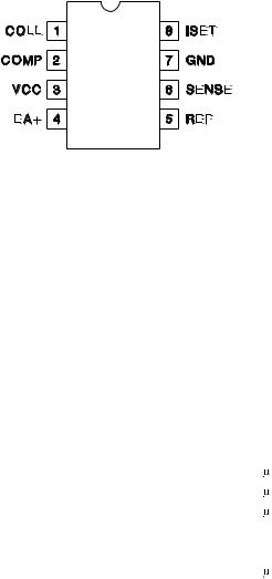
CONNECTION DIAGRAM |
|
|
|
|
|
|
|
UC39432B |
||||||||||||||
|
|
|
|
|
|
|
|
|
|
|
|
|
|
|
||||||||
DIL-8, SOIC-8 (Top View) |
|
|
|
|
|
|
|
|
|
|
|
|
||||||||||
N or J, D Package |
|
|
|
|
|
|
|
|
|
|
|
|
||||||||||
|
|
|
|
|
|
|
|
|
|
|
|
|
|
|
|
|
|
|
|
|
|
|
|
|
|
|
|
|
|
|
|
|
|
|
|
|
|
|
|
|
|
|
|
|
|
|
|
|
|
|
|
|
|
|
|
|
|
|
|
|
|
|
|
|
|
|
|
|
|
|
|
|
|
|
|
|
|
|
|
|
|
|
|
|
|
|
|
|
|
|
|
ELECTRICAL CHARACTERISTICS: Unless otherwise stated, these specifications apply for TA = –55°C to +125°C and COLL Output = 2.4V to 36.0V for the UC19432, TA = –25°C to +85°C and COLL Output = 2.3V to 36.0V for the UC29432, and T A = 0°C to +70°C and COLL Output = 2.3V to 36.0V for the UC39432, VCC = 15V, I COLL = 10mA, TA = TJ.
PARAMETER |
TEST CONDITIONS |
|
MIN |
TYP |
MAX |
UNITS |
Reference Voltage Tolerance |
TA = 25°C |
19432* |
1.295 |
1.3 |
1.305 |
V |
|
|
39432B |
1.29 |
1.3 |
1.31 |
V |
Reference Temperature Tolerance |
VCOLL = 5.0V |
19432* |
1.291 |
1.3 |
1.309 |
V |
|
|
39432B |
1.286 |
1.3 |
1.314 |
V |
Reference Line Regulation |
VCC = 2.4V to 36.0V, VCOLL = 5V |
19432* |
|
10 |
38 |
mV |
|
|
39432B |
|
10 |
57 |
mV |
Reference Load Regulation |
ICOLL = 10mA to 50mA, VCOLL = 5V |
19432* |
|
10 |
38 |
mV |
|
|
39432B |
|
10 |
57 |
mV |
Reference Sink Current |
|
|
|
|
10 |
A |
Reference Source Current |
|
|
|
|
–10 |
A |
EA Input Bias Current |
|
|
–0.5 |
–0.2 |
|
A |
EA Input Offset Voltage |
|
19432* |
|
|
4.0 |
mV |
|
|
39432B |
|
|
4.0 |
mV |
EA Output Current Sink (Internally Limited) |
|
|
|
|
16 |
A |
EA Output Current Source |
|
|
|
|
–1 |
mA |
Minimum Operating Current |
VCC = 36.0V, VCOLL = 5V |
|
|
0.50 |
0.80 |
mA |
Collector Current Limit (Note) |
VCOLL = VCC = 36.0V, Ref = 1.35V |
|
|
130 |
145 |
mA |
|
ISET = GND |
|
|
|
|
|
Collector Saturation |
ICOLL = 20mA |
|
0.7 |
1.1 |
1.5 |
V |
Transconductance (gm) (Note) |
VCC = 2.4V to 36.0V, |
19432* |
–170 |
–140 |
–110 |
mS |
|
VCOL = 3V, ICOLL = 20mA |
39432B |
–180 |
–140 |
–100 |
mS |
|
ISET = GND |
|
|
|
|
|
Error Amplifier AVOL |
|
|
60 |
90 |
|
dB |
Error Amplifier GBW |
(Note 1) |
|
3.0 |
5 |
|
MHz |
Transconductance Amplifier GBW |
|
|
|
3 |
|
MHz |
* Also applies to the UC29432 and UC39432
Note: Programmed transconductance and collector current limit equations are specified in the ISET pin description. Note 1: Guaranteed by design. Not 100% tested in production.
2
 Loading...