


Texas Instruments UCC3813PWTR-5, UCC3813PWTR-4, UCC3813PWTR-3, UCC3813D-2, UCC3813D-1 Datasheet
...
UCC2813-0/-1/-2/-3/-4/-5
UCC3813-0/-1/-2/-3/-4/-5
Low Power Economy BiCMOS Current Mode PWM
FEATURES
100 A Typical Starting Supply Current
500 A Typical Operating Supply Current
Operation to 1MHz
Internal Soft Start
Internal Fault Soft Start
Internal Leading-Edge Blanking of the
Current Sense Signal
1 Amp Totem-Pole Output
70ns Typical Response from Current-Sense to Gate Drive Output
1.5% Tolerance Voltage Reference
Same Pinout as UCC3802, UC3842, and
UC3842A
ORDERING INFORMATION
DESCRIPTION
The UCC3813-0/-1/-2/-3/-4/-5 family of high-speed, low-power integrated circuits contain all of the control and drive components required for off-line and DC-to-DC fixed frequency current-mode switching power supplies with minimal parts count.
These devices have the same pin configuration as the UC3842/3/4/5 family, and also offer the added features of internal full-cycle soft start and internal leading-edge blanking of the current-sense input.
The UCC3813-0/-1/-2/-3/-4/-5 family offers a variety of package options, temperature range options, choice of maximum duty cycle, and choice of critical voltage levels. Lower reference parts such as the UCC3813-3 and UCC3813-5 fit best into battery operated systems, while the higher reference and the higher UVLO hysteresis of the UCC3813-2 and UCC3813-4 make these ideal choices for use in off-line power supplies.
The UCC2813-x series is specified for operation from –40°C to +85°C and the UCC3813-x series is specified for operation from 0°C to +70°C.
Part Number |
Maximum Duty Cycle |
Reference Voltage |
Turn-On Threshold |
Turn-Off Threshold |
UCCx813-0 |
100% |
5V |
7.2V |
6.9V |
UCCx813-1 |
50% |
5V |
9.4V |
7.4V |
UCCx813-2 |
100% |
5V |
12.5V |
8.3V |
UCCx813-3 |
100% |
4V |
4.1V |
3.6V |
UCCx813-4 |
50% |
5V |
12.5V |
8.3V |
UCCx813-5 |
50% |
4V |
4.1V |
3.6V |
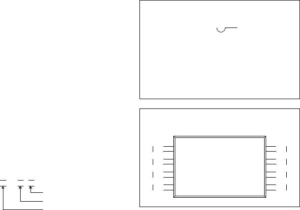
BLOCK DIAGRAM
UDG-96134 |
04/99 |
ABSOLUTE MAXIMUM RATINGS (Note 1)
VCC Voltage (Note 2) . . . . . . . . . . . . . . . . . . . . . . . . . . . 12.0V VCC Current . . . . . . . . . . . . . . . . . . . . . . . . . . . . . . . . . 30.0mA OUT Current . . . . . . . . . . . . . . . . . . . . . . . . . . . . . . . . . . 1.0A OUT Energy (Capacitive Load) . . . . . . . . . . . . . . . . . . . 20.0 J Analog Inputs (FB, CS) . . . . . . . . . . . . . . . . . . . . –0.3V to 6.3V Power Dissipation at TA < +25°C (N Package). . . . . . . . . 1.0W Power Dissipation at TA < +25°C (D Package). . . . . . . . 0.65W Storage Temperature . . . . . . . . . . . . . . . . . . . –65 C to +150°C Junction Temperature. . . . . . . . . . . . . . . . . . . –55 C to +150°C Lead Temperature (Soldering, 10 Seconds). . . . . . . . . +300°C
Note 1: All voltages are with respect to GND. All currents are positive into the specified terminal. Consult Unitrode Integrated Circuits databook for information regarding thermal specifications and limitations of packages.
Note 2: In normal operation VCC is powered through a current limiting resistor. Absolute maximum of 12V applies when VCC is driven from a low impedance source such that ICC does not exceed 30mA.
|
TEMPERATURE RANGE |
PACKAGES |
UCC2813 |
–40°C TO +85°C |
N, D, PW |
UCC3813 |
0°C TO +70°C |
N, D, PW |
ORDERING INFORMATION
UCC 
 813
813 
 –
– 

PRODUCT OPTION
PACKAGE
TEMPERATURE RANGE
UCC2813-0/-1/-2/-3/-4/-5
UCC3813-0/-1/-2/-3/-4/-5
CONNECTION DIAGRAMS
DIL-8 or SOIC-8 (TOP VIEW)
N or D PACKAGE
COMP |
|
|
|
|
REF |
1 |
|
|
8 |
||
|
|
|
|
|
VCC |
|
|
|
|
|
|
FB |
2 |
|
|
7 |
|
|
|
|
|
|
|
|
|
|
|
|
|
CS |
3 |
|
|
6 |
OUT |
|
|
|
|
|
GND |
|
|
|
|
|
|
RC |
4 |
|
|
5 |
|
|
|
|
|
|
|
|
|
|
|
|
|
TSSOP-8 (TOP VIEW) |
|
|
|
PW PACKAGE |
|
|
|
1 |
COMP |
REF |
8 |
2 |
FB |
VCC |
7 |
3 |
CS |
OUT |
6 |
4 |
RC |
GND |
5 |
ELECTRICAL CHARACTERISTICS Unless otherwise stated, these specifications apply for –40°C ≤ TA ≤ +85°C for UCC2813-x; 0°C ≤ TA ≤ +70°C for UCC3813-x; VCC = 10V (Note 3); RT = 100k from REF to RC; CT=330pF from RC to GND; 0.1 F capacitor from VCC to GND; 0.1 F capacitor from VREF to GND. TA = TJ.
|
|
UCC2813-x |
|
||
PARAMETER |
TEST CONDITIONS |
UCC3813-x |
UNITS |
||
|
|
MIN |
TYP |
MAX |
|
Reference Section |
|
|
|
|
|
Output Voltage |
TJ = +25°C, I = 0.2mA, UCCx813-0/-1/-2/-4 |
4.925 |
5.00 |
5.075 |
V |
|
TJ = +25°C, I = 0.2mA, UCCx813-5 |
3.94 |
4.00 |
4.06 |
V |
Load Regulation |
0.2mA < I < 5mA |
|
10 |
30 |
mV |
Total Variation |
UCCx813 -0-1/-2/-4 (Note 7) |
4.84 |
5.00 |
5.10 |
V |
|
UCCx813-5 (Note 7) |
3.84 |
4.00 |
4.08 |
V |
Output Noise Voltage |
10Hz ≤ f ≤ 10kHz, TJ = +25°C (Note 9) |
|
70 |
|
V |
Long Term Stability |
TA = +125 C, 1000 Hours (Note 9) |
|
5 |
|
mV |
Output Short Circuit |
|
–5 |
|
–35 |
mA |
Oscillator Section |
|
|
|
|
|
Oscillator Frequency |
UCCx813-0/-1/-2/-4 (Note 4) |
40 |
46 |
52 |
kHz |
|
UCCx813-5 (Note 4) |
26 |
31 |
36 |
kHz |
Temperature Stability |
(Note 9) |
|
2.5 |
|
% |
Amplitude Peak-to-Peak |
|
2.25 |
2.40 |
2.55 |
V |
Oscillator Peak Voltage |
|
|
2.45 |
|
V |
2
UCC2813-0/-1/-2/-3/-4/-5
UCC3813-0/-1/-2/-3/-4/-5
ELECTRICAL CHARACTERISTICS Unless otherwise stated, these specifications apply for –40°C ≤ TA ≤ +85°C for UCC2813-x; 0°C ≤ TA ≤ +70°C for UCC3813-x; VCC = 10V (Note 3); RT = 100k from REF to RC; CT=330pF from RC to GND; 0.1 F capacitor from VCC to GND; 0.1 F capacitor from VREF to GND. TA = TJ.
|
|
UCC2813-x |
|
||
PARAMETER |
TEST CONDITIONS |
UCC3813-x |
UNITS |
||
|
|
MIN |
TYP |
MAX |
|
Error Amplifier Section |
|
|
|
|
|
Input Voltage |
COMP = 2.5V; UCCx813-0/-1/-2/-4 |
2.42 |
2.50 |
2.56 |
V |
|
COMP = 2.0V; UCCx813-3/-5 |
1.92 |
2.0 |
2.05 |
V |
Input Bias Current |
|
–2 |
|
2 |
A |
Open Loop Voltage Gain |
|
60 |
80 |
|
dB |
COMP Sink Current |
FB = 2.7V, COMP = 1.1V |
0.4 |
|
2.5 |
mA |
COMP Source Current |
FB = 1.8V, COMP = REF – 1.2V |
–0.2 |
–0.5 |
–0.8 |
mA |
Gain Bandwidth Product |
(Note 9) |
|
2 |
|
MHz |
PWM Section |
|
|
|
|
|
Maximum Duty Cycle |
UCCx813-0/-2/-3 |
97 |
99 |
100 |
% |
|
UCCx813-1/-4/-5 |
48 |
49 |
50 |
|
Minimum Duty Cycle |
COMP = 0V |
|
|
0 |
% |
Current Sense Section |
|
|
|
|
|
Gain |
(Note 5) |
1.10 |
1.65 |
1.80 |
V/V |
Maximum Input Signal |
COMP = 5V (Note 6) |
0.9 |
1.0 |
1.1 |
V |
Input Bias Current |
|
–200 |
|
200 |
nA |
CS Blank Time |
|
50 |
100 |
150 |
ns |
Over-Current Threshold |
|
1.32 |
1.55 |
1.70 |
V |
COMP to CS Offset |
CS = 0V |
0.45 |
0.90 |
1.35 |
V |
Output Section |
|
|
|
|
|
OUT Low Level |
I = 20mA, all parts |
|
0.1 |
0.4 |
V |
|
I = 200mA, all parts |
|
0.35 |
0.90 |
V |
|
I = 50mA, VCC = 5V, UCCx813-3/-5 |
|
0.15 |
0.40 |
V |
|
I = 20mA, VCC = 0V, all parts |
|
0.7 |
1.2 |
V |
OUT High VSAT |
I = –20mA, all parts |
|
0.15 |
0.40 |
V |
(VCC-OUT) |
I = –200mA, all parts |
|
1.0 |
1.9 |
V |
|
I = –50mA,VCC = 5V, UCCx813-3/-5 |
|
0.4 |
0.9 |
V |
Rise Time |
CL = 1nF |
|
41 |
70 |
ns |
Fall Time |
CL = 1nF |
|
44 |
75 |
ns |
Undervoltage Lockout Section |
|
|
|
|
|
Start Threshold (Note 8) |
UCCx813-0 |
6.6 |
7.2 |
7.8 |
V |
|
UCCx813-1 |
8.6 |
9.4 |
10.2 |
V |
|
UCCx813-2/-4 |
11.5 |
12.5 |
13.5 |
V |
|
UCCx813-3/-5 |
3.7 |
4.1 |
4.5 |
V |
Stop Threshold (Note 8) |
UCC1813-0 |
6.3 |
6.9 |
7.5 |
V |
|
UCC1813-1 |
6.8 |
7.4 |
8.0 |
V |
|
UCCx813-2/-4 |
7.6 |
8.3 |
9.0 |
V |
|
UCCx813-3/-5 |
3.2 |
3.6 |
4.0 |
V |
Start to Stop Hysteresis |
UCCx813-0 |
0.12 |
0.3 |
0.48 |
V |
|
UCCx813-1 |
1.6 |
2 |
2.4 |
V |
|
UCCx813-2/-4 |
3.5 |
4.2 |
5.1 |
V |
|
UCCx813-3/-5 |
0.2 |
0.5 |
0.8 |
V |
3
 Loading...