


Texas Instruments UC3847J, UC3847DWTR, UC3847DW, UC3846QTR, UC3846Q Datasheet
...
UC1846/7
UC2846/7
UC3846/7
Current Mode PWM Controller
FEATURES
∙Automatic Feed Forward Compensation
∙Programmable Pulse-by-Pulse Current Limiting
∙Automatic Symmetry Correction in Push-pull Configuration
∙Enhanced Load Response Characteristics
∙Parallel Operation Capability for Modular Power Systems
∙Differential Current Sense Amplifier with Wide Common Mode Range
∙Double Pulse Suppression
∙500mA (Peak) Totem-pole Outputs
∙±1% Bandgap Reference
∙Under-voltage Lockout
∙Soft Start Capability
∙Shutdown Terminal
∙500kHZ Operation
DESCRIPTION
The UC1846/7 family of control ICs provides all of the necessary features to implement fixed frequency, current mode control schemes while maintaining a minimum external parts count. The superior performance of this technique can be measured in improved line regulation, enhanced load response characteristics, and a simpler, easier-to-design control loop. Topological advantages include inherent pulse-by-pulse current limiting capability, automatic symmetry correction for push-pull converters, and the ability to parallel “power modules" while maintaining equal current sharing.
Protection circuitry includes built-in under-voltage lockout and programmable current limit in addition to soft start capability. A shutdown function is also available which can initiate either a complete shutdown with automatic restart or latch the supply off.
Other features include fully latched operation, double pulse suppression, deadline adjust capability, and a ±1% trimmed bandgap reference.
The UC1846 features low outputs in the OFF state, while the UC1847 features high outputs in the OFF state.
BLOCK DIAGRAM
1/97 |
UC1846/7
UC2846/7
UC3846/7
ABSOLUTE MAXIMUM RATINGS (Note 1)
Supply Voltage (Pin 15) . . . . . . . . . . . . . . . . . . . . . . . . . . . . . . . . . . . . . . . . . +40V
Collector Supply Voltage (Pin 13). . . . . . . . . . . . . . . . . . . . . . . . . . . . . . . . . . +40V Output Current, Source or Sink (Pins 11, 14). . . . . . . . . . . . . . . . . . . . . . . . 500mA Analog Inputs (Pins 3, 4, 5, 6, 16) . . . . . . . . . . . . . . . . . . . . . . . . . . . -0.3V to +VIN Reference Output Current (Pin 2). . . . . . . . . . . . . . . . . . . . . . . . . . . . . . . . . -30mA Sync Output Current (Pin 10) . . . . . . . . . . . . . . . . . . . . . . . . . . . . . . . . . . . . . -5mA Error Amplifier Output Current (Pin 7) . . . . . . . . . . . . . . . . . . . . . . . . . . . . . . -5mA Soft Start Sink Current (Pin 1) . . . . . . . . . . . . . . . . . . . . . . . . . . . . . . . . . . . . 50mA Oscillator Charging Current (Pin 9) . . . . . . . . . . . . . . . . . . . . . . . . . . . . . . . . . 5mA Power Dissipation at TA=25°C . . . . . . . . . . . . . . . . . . . . . . . . . . . . . . . . . 1000mW Power Dissipation at TC=25°C . . . . . . . . . . . . . . . . . . . . . . . . . . . . . . . . . 2000mW Storage Temperature Range . . . . . . . . . . . . . . . . . . . . . . . . . . . . -65°C to +150°C Lead Temperature (soldering, 10 seconds. . . . . . . . . . . . . . . . . . . . . . . . . +300°C
Note 1. All voltages are with respect to Ground, Pin 13. Currents are positive into, negative out of the speficied terminal. Consult Packaging Section of Databook for thermal limitations and considerations of packages. Pin numbers refer to DIL and SOIC packages only.
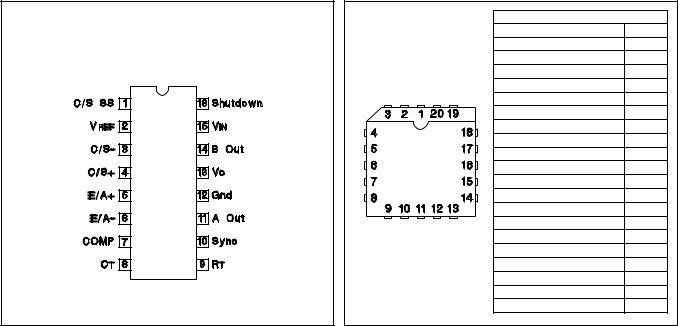
CONNECTION DIAGRAMS
DIL-16, SOIC-16 |
PLCC-20, LCC-20 |
PACKAGE PIN FUNCTION |
||
(TOP VIEW) |
(TOP VIEW) |
|||
FUNCTION |
PIN |
|||
J or N Package, DW Package |
Q, L Packages |
N/C |
1 |
|
|
|
C/L SS |
2 |
|
|
|
VREF |
3 |
|
|
|
C/S- |
4 |
|
|
|
C/S+ |
5 |
|
|
|
N/C |
6 |
|
|
|
E/A+ |
7 |
|
|
|
E/A- |
8 |
|
|
|
Comp |
9 |
|
|
|
CT |
10 |
|
|
|
N/C |
11 |
|
|
|
RT |
12 |
|
|
|
Sync |
13 |
|
|
|
A Out |
14 |
|
|
|
Gnd |
15 |
|
|
|
N/C |
16 |
|
|
|
VC |
17 |
|
|
|
B Out |
18 |
|
|
|
VIN |
19 |
|
|
|
Shutdown |
20 |
|
ELECTRICAL CHARACTERISTICS (Unless otherwise stated, these specifications apply for TA=-55°C to +125°C for UC1846/7; -40°C to +85°C for the UC2846/7; and 0°C to +70°C for the UC3846/7;
VIN=15V, RT=10k, CT=4.7nF, TA=TJ.)
|
|
UC1846/UC1847 |
UC3846/UC3847 |
|
||||
PARAMETER |
TEST CONDITIONS |
UC2846/UC2847 |
|
|||||
|
|
|
|
|||||
|
|
MIN. |
TYP. |
MAX. |
MIN. |
TYP. |
MAX. |
UNITS |
Reference Section |
|
|
|
|
|
|
|
|
Output Voltage |
TJ=25°C, I O=1mA |
5.05 |
5.10 |
5.15 |
5.00 |
5.10 |
5.20 |
V |
Line Regulation |
VIN=8V to 40V |
|
5 |
20 |
|
5 |
20 |
mV |
Load Regulation |
IL=1mA to 10mA |
|
3 |
15 |
|
3 |
15 |
mV |
Temperature Stability |
Over Operating Range, (Note 2) |
|
0.4 |
|
|
0.4 |
|
mV/°C |
Total Output Variation |
Line, Load, and Temperature (Note 2) |
5.00 |
|
5.20 |
4.95 |
|
5.25 |
V |
Output Noise Voltage |
10Hz≤ f ≤10kHz, TJ=25°C (Note 2) |
|
100 |
|
|
100 |
|
μV |
Long Term Stability |
TJ=125°C, 1000 Hrs. (Note 2) |
|
5 |
|
|
5 |
|
mV |
Short Circuit Output Current |
VREF=0V |
-10 |
-45 |
|
-10 |
-45 |
|
mA |
2
ELECTRICAL
CHARACTERISTICS (cont.)
UC1846/7
UC2846/7
UC3846/7
(Unless otherwise stated, these specifications apply for TA=-55°C to +125°C for UC1846/7; -40°C to +85°C for the UC2846/7; and 0°C to +70°C for the UC3846/7; V IN=15V, RT=10k, CT=4.7nF, TA=TJ.)
|
|
UC1846/UC1847 |
UC3846/UC3847 |
|
||||
PARAMETER |
TEST CONDITIONS |
UC2846/UC2847 |
|
|||||
|
|
|
|
|||||
|
|
MIN. |
TYP. |
MAX. |
MIN. |
TYP. |
MAX. |
UNITS |
Oscillator Section |
|
|
|
|
|
|
|
|
Initial Accuracy |
TJ=25°C |
39 |
43 |
47 |
39 |
43 |
47 |
kHz |
Voltage Stability |
VIN=8V to 40V |
|
-1 |
2 |
|
-1 |
2 |
% |
Temperature Stability |
Over Operating Range (Note 2) |
|
-1 |
|
|
-1 |
|
% |
Sync Output High Level |
|
3.9 |
4.35 |
|
3.9 |
4.35 |
|
V |
Sync Output Low Level |
|
|
2.3 |
2.5 |
|
2.3 |
2.5 |
V |
Sync Input High Level |
Pin 8=0V |
3.9 |
|
|
3.9 |
|
|
V |
Sync Input Low Level |
Pin 8=0V |
|
|
2.5 |
|
|
2.5 |
V |
Sync Input Current |
Sync Voltage=3.9V, Pin 8=0V |
|
1.3 |
1.5 |
|
1.3 |
1.5 |
mA |
Error Amp Section |
|
|
|
|
|
|
|
|
Input Offset Voltage |
|
|
0.5 |
5 |
|
0.5 |
10 |
mV |
Input Bias Current |
|
|
-0.6 |
-1 |
|
-0.6 |
-2 |
μA |
Input Offset Current |
|
|
40 |
250 |
|
40 |
250 |
nA |
Common Mode Range |
VIN=8V to 40V |
0 |
|
VIN-2V |
0 |
|
VIN-2V |
V |
Open Loop Voltage Gain |
VO=1.2 to 3V, VCM=2V |
80 |
105 |
|
80 |
105 |
|
dB |
Unity Gain Bandwidth |
TJ=25°C (Note 2) |
0.7 |
1.0 |
|
0.7 |
1.0 |
|
MHz |
CMRR |
VCM=0V to 38V, VIN=40V |
75 |
100 |
|
75 |
100 |
|
dB |
PSRR |
VIN=8V to 40V |
80 |
105 |
|
80 |
105 |
|
dB |
Output Sink Current |
VID=-15mV to -5V, VPIN 7=1.2V |
2 |
6 |
|
2 |
6 |
|
mA |
Output Source Current |
VID=15mV to 5V, VPIN 7=2.5V |
-0.4 |
-0.5 |
|
-0.4 |
-0.5 |
|
mA |
High Level Output Voltage |
RL=(Pin 7) 15kΩ |
4.3 |
4.6 |
|
4.3 |
4.6 |
|
V |
Low Level Output Voltage |
|
|
0.7 |
1 |
|
0.7 |
1 |
V |
Current Sense Amplifier Section |
|
|
|
|
|
|
|
|
Amplifier Gain |
VPIN 3=0V, Pin 1 Open (Notes 3 & 4) |
2.5 |
2.75 |
3.0 |
2.5 |
2.75 |
3.0 |
V |
Maximum Differential Input |
Pin 1 Open (Note 3) |
|
|
|
|
|
|
|
Signal (VPIN 4-VPIN 3) |
RL (Pin 7)=15kW |
1.1 |
1.2 |
|
1.1 |
1.2 |
|
V |
Input Offset Voltage |
VPIN 1=0.5V, Pin 7 Open (Note 3) |
|
5 |
25 |
|
5 |
25 |
mV |
CMRR |
VCM=1V to 12V |
60 |
83 |
|
60 |
83 |
|
dB |
PSRR |
VIN=8V to 40V |
60 |
84 |
|
60 |
84 |
|
dB |
Input Bias Current |
VPIN 1=0.5V, Pin 7 Open (Note 3) |
|
-2.5 |
-10 |
|
-2.5 |
-10 |
μA |
Input Offset Current |
VPIN 1=0.5V, Pin 7 Open (Note 3) |
|
0.08 |
1 |
|
0.08 |
1 |
μA |
Input Common Mode Range |
|
0 |
|
VIN-3 |
0 |
|
VIN-3 |
V |
Delay to Outputs |
TJ=25°C, (Note 2) |
|
200 |
500 |
|
200 |
500 |
ns |
Current Limit Adjust Section |
|
|
|
|
|
|
|
|
Current Limit Offset |
VPIN 3=0V, VPIN 4=0V, Pin 7 Open |
|
|
|
|
|
|
|
|
(Note 3) |
0.45 |
0.5 |
0.55 |
0.45 |
0.5 |
0.55 |
V |
Input Bias Current |
VPIN 5=VREF, VPIN 6=0V |
|
-10 |
-30 |
|
-10 |
-30 |
μA |
Shutdown Terminal Section |
|
|
|
|
|
|
|
|
Threshold Voltage |
|
250 |
350 |
400 |
250 |
350 |
400 |
mV |
Input Voltage Range |
|
0 |
|
VIN |
0 |
|
VIN |
V |
Minimum Latching Current |
(Note 6) |
|
|
|
|
|
|
|
(IPIN 1) |
|
3.0 |
1.5 |
|
3.0 |
1.5 |
|
mA |
3
 Loading...