


UC3702N
UC1702
UC2702
UC3702
DESCRIPTION
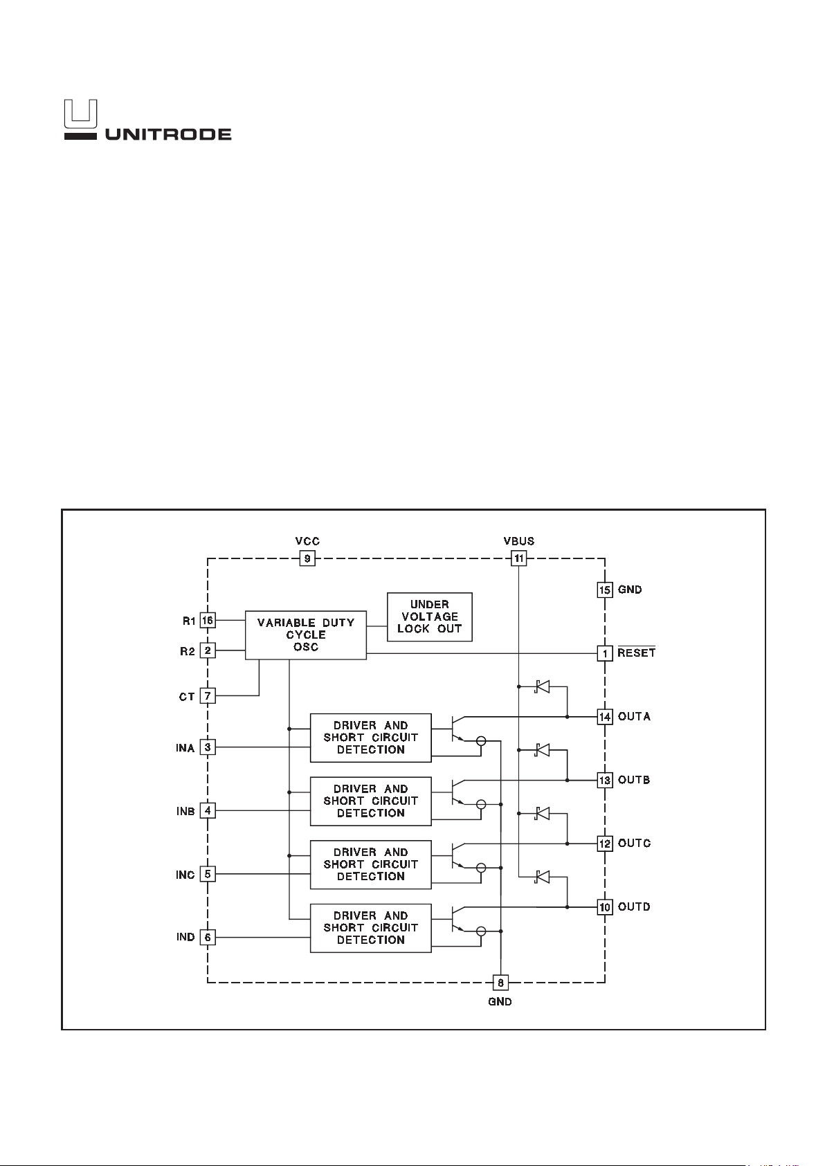
The UC3702 Quad Relay Driver is intended to drive up to four relays from
logic inputs using an unregulated relay voltage supply. The relays are
driven from the Bus supply in a power efficient PWM converter fashion.
The relay coil is used as the inductive element. (See the application's sec
tion concerning the relay selection.) VBUS must be higher then the rated
relay voltage. Short circuit protection is provided on chip with periodic retry.
The UC3702 requires a +5V logic supply as a reference. Two external re
sistors program the effective relay voltage and a capacitor sets the nominal
operating frequency. Internal Schottky diodes eliminate the need for any
external power components.
In typical applications, the UC3702 grants the user the flexibility to choose
the most cost effective relay without the added burden of generating a sep
arate relay supply voltage. The UC3702 will even function with a poorly
regulated supply VBUS, containing significant 100Hz or 120Hz ripple.
Quad PWM Relay Driver
FEATURES
•
Maintains Constant Average
Relay Voltage With Varying
Supply Voltages
•
VBUS Voltages up to 42.5V
•
Up to 50mA per Relay
•
Integrated Schottky Flyback Diodes
•
Individual Relay Control Inputs
•
Short Circuit Protection
•
User Selectable Operating Center
Frequency and Relay Voltage
•
Global Reset
SLUS368 - APRIL 1997
BLOCK DIAGRAM
UDG-96009-1
2
UC1702
UC2702
UC3702
ABSOLUTE MAXIMUM RATINGS
VBUS. . . . . . . . . . . . . . . . . . . . . . . . . . . . . . . . . . . . . . . . . +50V
VCC. . . . . . . . . . . . . . . . . . . . . . . . . . . . . . . . . . . . . . . . . . . +9V
Input Voltage . . . . . . . . . . . . . . . . . . . . . . –0.3V to VCC + 0.3V
Average Current per Relay. . . . . . . . . . . . . . . . . . . . . . . . 50mA
Total Output Capacitance. . . . . . . . . . . . . . . . . . . . . . . . . 25pF
Storage Temperature . . . . . . . . . . . . . . . . . . . –65°C to +150°C
Junction Temperature. . . . . . . . . . . . . . . . . . . –55°C to +150°C
Lead Temperature (Soldering, 10 sec.) . . . . . . . . . . . . . +300°C
Currents are positive into, negative out of the specified termi
-
nal. Consult Packaging Section of Databook for thermal limita
-
tions and considerations of packages.
ELECTRICAL CHARACTERISTICS: Unless otherwise stated these specifications apply for T
A
= –55°C to +125°C for
UC1702; –25°C to +85°C for UC2702; 0°C to +70°C for UC3702; VBUS = 34V, VCC = 5V, RESET
= VCC, R2 = 43.2k ;
R1 = 203k
; CT = 220pF, TA= TJ.
PARAMETER
TEST CONDITIONS MIN TYP MAX UNITS
Supply Voltage Section
VCC 4.5 5 8 V
VCC Supply Current RESET
, INA, INB, INC, IND = VCC 4 6 mA
VBUS 42.5 V
Oscillator Section
NOMINAL Operating Frequency R1 = 203k
, R2 = 43.2k , CT = 220pF 150 175 200 kHz
R1 100 202 500 k
R2 20 42.5 80 k
CT 100 pF
Output Driver VBUS = 20V
Rated Relay Current 50 mA
Short Circuit Current 100 175 mA
Diode Leakage Current Control Input Low, V
OUTX
= VBUS 0.05 5 A
Diode Forward Voltage 500 mV
Averaged Output Voltage Error UC2702, UC3702 (Note 1) –10 10 %
UC1702 –20 20 %
Control Inputs (INA, INB, INC, IND)
Logic Low 0.5 V
Logic High 3 VCC V
TON / TOFF Delay 250 ns
Input Current –1 0 1
A
Input Current V
IN
= 5V 70 120 A
RESET
TON / TOFF Delay 2 s
Input Current V
IN
= 0.3V –8 –5 A
Input Current V
IN
= 5V –10 0 10 A
Note 1: Programmed Average Voltage
=
••
•
106 1
22
400
.
–
RVCC
R
mV
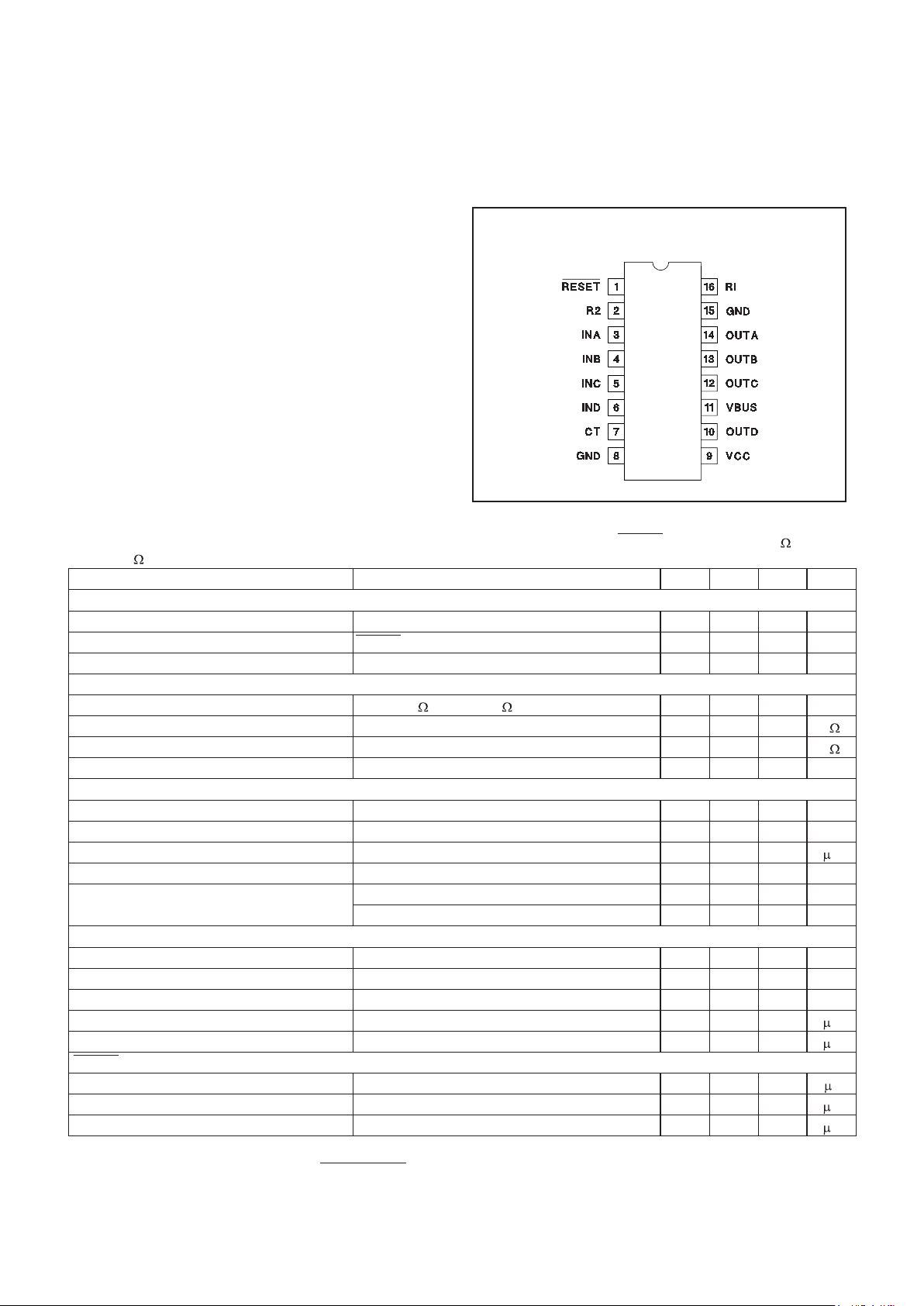
CONNECTION DIAGRAM
DIL-16, SOIC-16 (Top View)
J or N, D Package
 Loading...