


UC3584DW
Texas Instruments UC3584DW, UC3578N, UC3578DPTR, UC3578DP, UC2578N Datasheet
...
UC2578
UC3578
05/99
FEATURES
• Provides Simple Single Inductor Buck
PWM Step-Down Voltage Regulation
• Drives External High Side NMOS
Switch
• 14V to 72V Input Voltage Operating
Range
• Contains 100kHz Internal Oscillator,
2V Reference and UVLO
• Soft Start on Power Up
• Overcurrent Shutdown Followed by
Soft Start
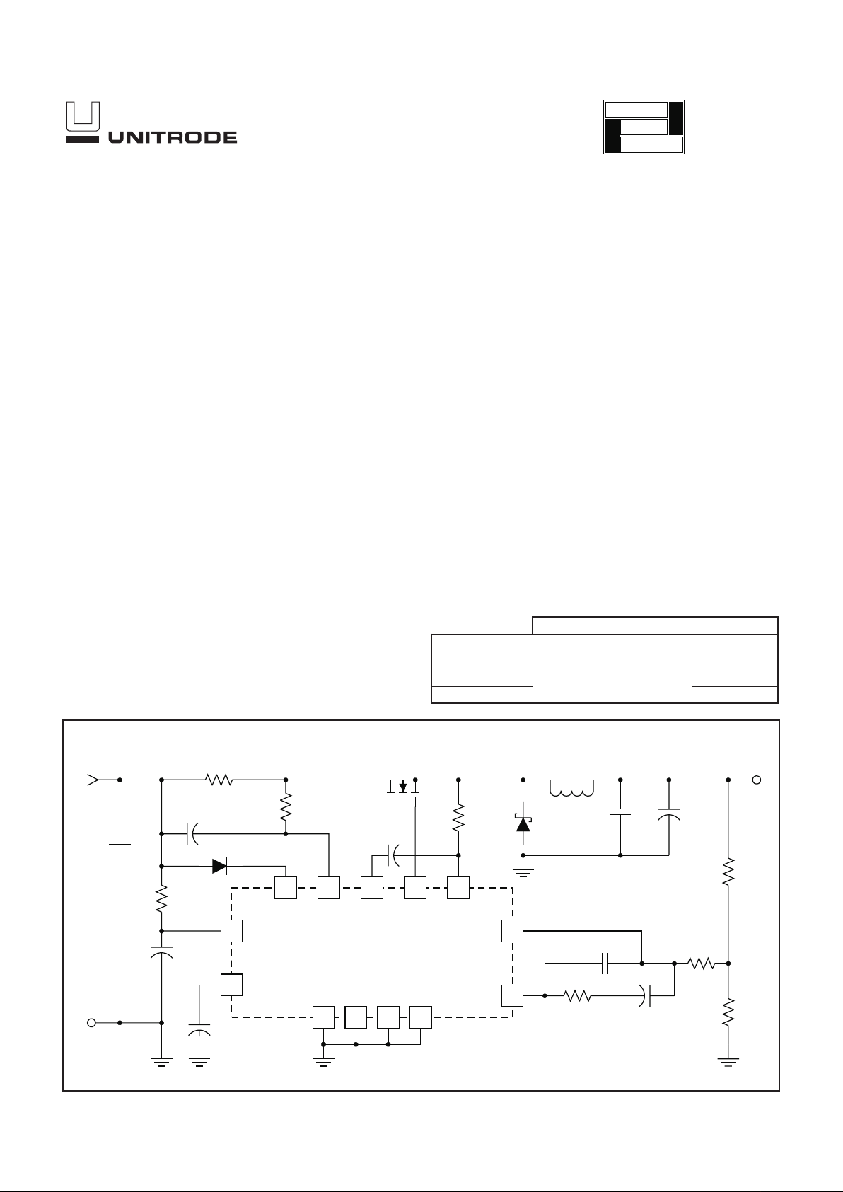
Buck Pulse Width Modulator Stepdown Voltage Regulator
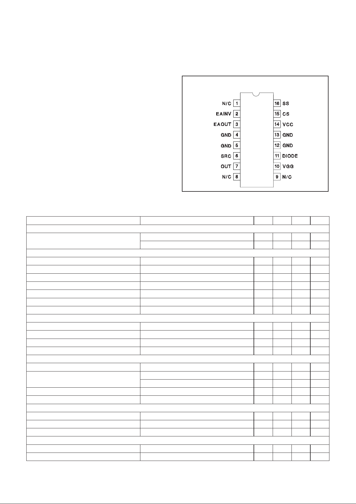
14
16
11 15 10 7 6
2
3
131254
EAINV
EAOUTGNDGND
SRCOUT
SS
CS
VCC
GND GND
DIODE VGG
UC3578
C
SS
2200pF
100k
220pF
50k
R1
1k
5k
C
GG
1µF
15
C
CC
1µF
47µF
10
1N4148
C
S
1000pF
R
S
1k
R
SENSE
0.12
IRFZ34
15-40 V
IN
1µF
C
OUT
220µF
L
OUT
40µH
RECTIFIER
MBR 3100
V
OUT
TYPICAL APPLICATION DIAGRAM
UDG-99064
DESCRIPTION
The UC3578 is a PWM controller with an integrated high side floating gate
driver. It is used in buck step down converters and regulates a positive
output voltage. Intended to be used in a distributed power system, the IC
allows operation from 14V to 72V input voltage which range includes the
prevalent telecomm bus voltages. The output duty cycle of the UC3578
can vary between 0% and 90% for operation over the wide input voltage
and load conditions.
The UC3578 simplifies the design of the single switch PWM buck converter
by incorporating a floating high side driver for an external N-channel
MOSFET switch. It also features a 100kHz fixed frequency oscillator, an
internal 2V precision reference, an error amplifier configured for voltage
mode operation, and a PWM comparator with latching logic. Comple-
menting the traditional voltage mode control block, the UC3578 incorpo-
rates an overcurrent shutdown circuit with full cycle soft re-start to limit the
input current to a user defined maximum value during overload operation.
Additional functions include an under voltage lockout circuit to insure that
sufficient input supply voltage is present before any switching activity can
occur.
The UC2578 and the UC3578 are both available in surface mount and
thru-hole power packages.
TEMPERATURE RANGE PACKAGE
UC2578DP –40°C to +85°C Power SOIC
UC2578N Power PDIP
UC3578DP 0°C to +70°C Power SOIC
UC3578N Power PDIP
ORDERING INFORMATION
application
INFO
available
2
UC2578
UC3578
ELECTRICAL CHARACTERISTICS:
Unless otherwise specified VCC = 14V, VGG = 14V, T
A
=T
J
.
PARAMETER TEST CONDITIONS MIN TYP MAX UNITS
Oscillator Section
Frequency VCC = 14V to 72V, EAINV = 1.9V, T
J
= 25°C 100 110 120 kHz
VCC = 11V to 14V, Over Temperature 90 120 kHz
Error Amplifier Section
EAINV EAOUT = EAINV 1.97 2 2.03 V
I
EAINV
EAOUT = EAINV 100 300 nA
EAVOL EAOUT/EAINV, 25°C 70 80 dB
EAOUT High EAINV ≤ 1.9V, I
EAOUT
= –100µA 5.5 6.2 V
EAOUT Low EAINV ≥ 2.1V, I
EAOUT
= 100µA 0.8 1.1 V
Unity Gain Bandwidth T
J
= 25°C, F = 100kHz 0.85 1 MHz
PSRR, EAOUT EAOUT = EAINV, VCC = 14V 80 90 dB
Current Sense Comparator Section
Threshold (Referred to VCC) 0.4 0.5 0.6 V
Input Bias Current CS = VCC – 0.4V 0.2 1 µA
Propagation Delay V
OVERDRIVE
= 250mV 0.7 1.2 µs
Blanking Time V
OVERDRIVE
= 250mV 75 200 300 ns
Gate Drive Output Section
VOH I
OUT
= –200mA 9.5 11 V
VOL I
OUT
= 20mA 0.2 0.36 V
I
OUT
= 200mA 1.5 2 V
Rise Time T
J
= 25°C, C
LOAD
= 1nF 40 70 ns
Fall Time T
J
= 25°C, C
LOAD
= 1nF 40 70 ns
Pulse Width Modulator Section
Maximum Duty Cycle EAINV ≤ 1.9V 85 90 %
Minimum Duty Cycle EAINV ≥ 2.1V 0 %
Modulator Gain EAOUT = 2.5V to 3.5V 30 %/V
Undervoltage Lockout Section
Start Threshold OUT – SRC, EAINV ≤ 1.9V, SRC = 0V 10 11 12 V
UVLO Hysteresis 1.5 2 2.5 V
CONNECTION DIAGRAM
Note: The four GND pins are internally connected.
DIL-16, SOIC-16 (Top View)
N or DP Packages
VCC. . . . . . . . . . . . . . . . . . . . . . . . . . . . . . . . . . . . . . . . . . +72V
EAINV . . . . . . . . . . . . . . . . . . . . . . . . . . . . . . . . . –0.3V to +10V
EAOUT . . . . . . . . . . . . . . . . . . . . . . . . . . . . . . . . –0.3V to +10V
SS . . . . . . . . . . . . . . . . . . . . . . . . . . . . . . . . . . . . –0.3V to +10V
DIODE . . . . . . . . . . . . . . . . . . . . . . . . . . . . . . . . . –0.3V to VCC
VGG . . . . . . . . . . . . . . . . . . . . . . . . . . . . . . –0.3V to VCC +14V
CS. . . . . . . . . . . . . . . . . . . . . . . . . . . . VCC – 5V to VCC +0.6V
I
OUT
Pulsed . . . . . . . . . . . . . . . . . . . . . . . . . . . . –0.8A to +0.6A
SRC . . . . . . . . . . . . . . . . . . . . . . . . . . . . . . . . . . . –0.6V to VCC
Storage Temperature . . . . . . . . . . . . . . . . . . . −65°C to +150°C
Junction Temperature. . . . . . . . . . . . . . . . . . . –55°C to +150°C
Lead Temperature (Soldering, 10 sec.). . . . . . . . . . . . . +300°C
Currents are positive into, negative out of the specified terminal.
Consult Packaging Section of Databook for thermal limitations
and considerations of packages.
ABSOLUTE MAXIMUM RATINGS
3
UC2578
UC3578
ELECTRICAL CHARACTERISTICS:
Unless otherwise specified VCC = 14V, VGG = 14V, T
A
=T
J
.
PARAMETER TEST CONDITIONS MIN TYP MAX UNITS
VGG Regulator Section
VGG – SRC VCC = 72V, SRC = 0V, I
VGG
= –7mA 14.5 15.25 17 V
VCC = 50V, SRC = 0V, I
VGG
= –7mA 14 14.75 16 V
VCC = 15V, SRC = 0V, I
VGG
= –7mA 13 13.75 14.5 V
VCC = 11V, SRC = 0V, I
VGG
= –7mA 9.5 10 10.5 V
Soft Start Ramp Section
Soft Start Ramp Current –30 –45 µA
Supply Current Section
I
VCC
EAINV ≥ 2.1V, SRC = 0V 10 14 mA
I
VGG
EAINV ≥ 2.1V, SRC = 0V 7 10.5 mA
CS: Peak current limit sense pin. Senses the current
across a current sense resistor placed between VCC and
the drain of the NMOS buck switch. OUT will be held low
(NMOS buck switch off) if VCC – CS exceeds 0.5V.
DIODE: An external small signal diode (1N4148 typical)
is connected here, anode to VCC and cathode to
DIODE, to implement the VGG regulator function.
EAINV: Inverting input to error amplifier. V
OUT
sense
feedback is connected to this pin. The non-inverting input
of the error amplifier is internally connected to 2V.
EAOUT: Output of the error amplifier. Use EAOUT and
EAINV for loop compensation components.
GND: Circuit Ground. The four ground pins are internally
connected together by the fused leadframe of the
package. They provide the primary thermal conduction
path for dissipating junction heat.
OUT: Gate drive for the external NMOS switch
connected between VCC and the buck inductor.
SRC: This pin is connected to the junction of the external
NMOS switch source, the floating voltage source
capacitor, the free-wheeling diode cathode, and buck
inductor.
SS: The external soft start capacitor is connected to this
pin.
VGG: An external capacitor connected from VGG to
SRC completes the floating voltage source for the
floating gate driver. A1µF capacitor is recommended.
VCC: Input supply voltage. This pin supplies an internal
ground referenced voltage regulator that supplies the IC
and an on-chip regulated floating voltage source (VGG –
SRC) used by the floating driver to drive the external
NMOS buck switch. This pin should be bypassed with a
high quality ceramic capacitor.
PIN DESCRIPTIONS
The UC3578 Floating Buck Controller is a high frequency
switching regulator with a floating driver which provides
PWM control for non-isolated buck converters. The con-
troller operates at a fixed 100 kHz switching frequency,
and in voltage mode control. The duty cycle range of the
PWM output is 0% to 90% allowing for a wide range of
input voltages (14V minimum with transients to 72V).
The regulator features an undervoltage lockout threshold
of 11V with approximately 2V hysterisis as well as soft
start capability. The typical application circuit shown is for
a 15V to 40V input and a 12V at 3A output.
To ensure proper operation of the floating driver, an ex-
ternal capacitor (1µF ceramic) must be connected from
VGG to SRC, and to the source of the external MOSFET
through a small resistor, as shown in the typical applica-
tion diagram and in Fig 2. This capacitor provides the en-
ergy for the high side driver. The gate drive voltage to
the MOSFET is internally regulated to 14V. A diode
(1N4148) is required from the input voltage to DIODE.
This allows the floating drive capacitor to charge during
conduction of the output rectifier but prevents its dis-
charge back into the supply rail. A 1µF ceramic capacitor
is recommended from VCC to ground to provide high fre-
quency decoupling. Additional decoupling of this pin
could be accomplished by a low value resistor between
VCC and V
IN
anda1µF capacitor from VCC to GND as
shown in the schematic.
APPLICATION INFORMATION
 Loading...