


Texas Instruments UC3573N, UC3573DTR, UC3573D, UC2573J, UC2573N Datasheet
...
UC1573
UC2573
UC3573
Buck Pulse Width Modulator Stepdown Voltage Regulator
FEATURES
∙Simple Single Inductor Buck PWM Stepdown Voltage Regulation
∙Drives External PMOS Switch
∙Contains UVLO Circuit
∙Includes Pulse-by-Pulse Current Limit
∙Low 50μA Sleep Mode Current
DESCRIPTION
The UC3573 is a Buck pulse width modulator which steps down and regulates a positive input voltage. The chip is optimized for use in a single inductor buck switching converter employing an external PMOS switch. The block diagram consists of a precision reference, an error amplifier configured for voltage mode operation, an oscillator, a PWM comparator with latching logic, and a 0.5A peak gate driver. The UC3573 includes an undervoltage lockout circuit to insure sufficient input supply voltage is present before any switching activity can occur, and a pulse-by-pulse current limit. Input current can be sensed and limited to a user determined maximum value. In addition, a sleep comparator interfaces to the UVLO circuit which turns the chip off when the input voltage is below the UVLO threshold. This reduces the supply current to only 50μA, making the UC3573 ideal for battery powered applications.
BLOCK DIAGRAM
UDG-94106-1 |
SLUS346 - APRIL 1999 |
ABSOLUTE MAXIMUM RATINGS
VCC . . . . . . . . . . . . . . . . . . . . . . . . . . . . . . . . . . . . . . . . . . . 35V EAINV . . . . . . . . . . . . . . . . . . . . . . . . . . . . . . . . . –0.6V to VCC
IEAOUT . . . . . . . . . . . . . . . . . . . . . . . . . . . . . . . . . . . . . . . . 25mA RAMP . . . . . . . . . . . . . . . . . . . . . . . . . . . . . . . . . . . –0.3V to 4V
CS . . . . . . . . . . . . . . . . . . . . . . . . . . . . . . . . . . . . –0.3V to VCC
IOUT . . . . . . . . . . . . . . . . . . . . . . . . . . . . . . . . . . . –0.7A to 0.7A I3VREF . . . . . . . . . . . . . . . . . . . . . . . . . . . . . . . . . . . . . . . –15mA Storage Temperature . . . . . . . . . . . . . . . . . . . –65°C to +150°C
Junction Temperature. . . . . . . . . . . . . . . . . . . –65°C to +150°C Lead Temperature (Soldering, 10 sec.) . . . . . . . . . . . . . +300°C
Currents are positive into, negative out of the specified terminal. Consult Packaging Section of Databook for thermal limitations and considerations of packages.
UC1573
UC2573
UC3573
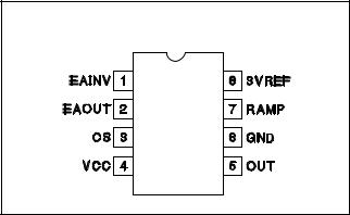
CONNECTION DIAGRAMS
DIL-8, SOIC-8 (TOP VIEW)
J or N, D Packages
ELECTRICAL CHARACTERISTICS: Unless otherwise specified, these parameters apply for TA = –55°C to +125°C for the UC1573, –40°C to +85°C for the UC2573, and 0°C to +70°C for the UC3573, VCC = 5V, CT = 680pF, T A = TJ.
PARAMETER |
TEST CONDITIONS |
MIN |
TYP |
MAX |
UNITS |
Reference Section |
|
|
|
|
|
3VREF |
|
2.94 |
3 |
3.06 |
V |
Line Regulation |
VCC = 4.75 to 30V |
|
1 |
10 |
mV |
Load Regulation |
I3VREF = 0 to –5mA |
|
1 |
10 |
mV |
Oscillator Section |
|
|
|
|
|
Frequency |
VCC = 5V, 30V |
85 |
100 |
115 |
kHz |
Error Amp Section |
|
|
|
|
|
EAINV |
EAOUT = 2V |
1.45 |
1.5 |
1.55 |
V |
IEAINV |
EAOUT = 2V |
|
–0.2 |
–1 |
μA |
AVOL |
EAOUT = 0.5V to 3V |
65 |
90 |
|
dB |
EAOUT High |
EAINV = 1.4V |
3.6 |
4 |
4.4 |
V |
EAOUT Low |
EAINV = 1.6V |
|
0.1 |
0.2 |
V |
IEAOUT |
EAINV = 1.4V, EAOUT = 2V |
–350 |
–500 |
|
μA |
|
EAINV = 1.6V, EAOUT = 2V |
7 |
20 |
|
mA |
Unity Gain Bandwidth |
TJ = 25°C, F = 10kHz |
0.6 |
1 |
|
MHz |
Current Sense Comparator Section |
|
|
|
|
|
Threshold (referred to VCC) |
|
–0.39 |
–0.43 |
–0.47 |
V |
Input Bias Current |
CS = VCC |
|
150 |
800 |
nA |
CS Propagation Delay |
|
|
400 |
|
ns |
Gate Drive Output Section |
|
|
|
|
|
OUT High Saturation |
IOUT = 0 |
|
0 |
0.3 |
V |
|
IOUT = –10mA |
|
0.7 |
1.5 |
V |
|
IOUT = –100mA |
|
1.5 |
2.5 |
V |
OUT Low Saturation |
IOUT = 10mA |
|
0.1 |
0.4 |
V |
|
IOUT = 100mA |
|
1.5 |
2.2 |
V |
Rise Time |
TJ = 25°C, C LOAD = 1nF + 3.3 Ohms |
|
30 |
80 |
ns |
Fall Time |
TJ = 25°C, C LOAD = 1nF + 3.3 Ohms |
|
30 |
80 |
ns |
Pulse Width Modulator Section |
|
|
|
|
|
Maximum Duty Cycle |
EAINV = 1.4V |
|
92 |
96 |
% |
Minimum Duty Cycle |
EAINV = 1.6V |
|
|
0 |
% |
Modulator Gain |
EAOUT = 1.5V to 2.5V |
25 |
35 |
45 |
%/V |
Undervoltage Lockout Section |
|
|
|
|
|
Start Threshold |
|
3.5 |
4.2 |
4.5 |
V |
Hysteresis |
|
100 |
200 |
300 |
mV |
2
 Loading...