


Texas Instruments THS4022IDR, THS4022IDGN, THS4022IDGNR, THS4022ID, THS4022EVM Datasheet
...THS4021, THS4022
350-MHz LOW-NOISE HIGH-SPEED AMPLIFIERS
SLOS265B ± SEPTEMBER 1999 ± REVISED FEBRUARY 2000
DUltra-Low 1.5 nV/√ Hz Voltage Noise
DHigh Speed
±350 MHz Bandwidth (G = 10, ±3 dB)
±470 V/µs Slew Rate
±40 ns Settling Time (0.1%)
DStable at a Gain of 10 (±9) or Greater
DHigh Output Drive, IO = 100 mA (typ)
DExcellent Video Performance
±17 MHz Bandwidth (0.1 dB, G = 10)
±0.02% Differential Gain
±0.08° Differential Phase
DVery Low Distortion
±THD = ±68 dBc (f = 1 MHz, RL = 150 Ω)
|
|
THS4021 |
|
|
|
THS4022 |
|
|||||||||||||||||
D AND DGN PACKAGE |
D AND DGN PACKAGE |
|||||||||||||||||||||||
|
|
(TOP VIEW) |
|
|
|
(TOP VIEW) |
|
|||||||||||||||||
NULL |
|
|
|
|
|
|
|
|
|
|
NULL |
1OUT |
|
|
|
|
|
|
|
|
|
|
|
VCC+ |
|
1 |
|
|
|
|
|
8 |
|
|
1 |
|
|
|
8 |
|
|||||||||
|
|
|
|
|
|
|
|
|
|
|
|
|||||||||||||
IN ± |
|
2 |
|
|
|
|
|
|
7 |
|
VCC+ |
1IN ± |
|
2 |
|
|
|
|
|
|
|
7 |
|
2OUT |
IN + |
|
3 |
|
|
|
|
|
|
6 |
|
OUT |
1IN + |
|
3 |
|
|
|
|
|
|
|
6 |
|
2IN± |
|
|
|
|
|
|
|
|
|
|
|
|
|||||||||||||
VCC± |
|
4 |
|
|
|
|
|
5 |
|
NC |
±VCC |
|
4 |
|
|
|
|
|
|
|
5 |
|
2IN+ |
|
|
|
|
|
|
|
|
|
|
|
|
|
|
|
|
|
|||||||||
|
|
|
|
|
|
|
|
|
|
|
|
|
|
|
|
|
|
|
|
|
|
|
||
|
|
|
|
|
|
|
|
|
|
|
|
|
|
|
|
|
|
|
|
|
|
|
|
|
NC ± No internal connection
Cross Section View Showing
PowerPAD Option (DGN)
VOLTAGE & CURRENT NOISE
DWide Range of Power Supplies
± VCC = ±5 V to ±15 V
DAvailable in Standard SOIC or MSOP PowerPAD Package
DEvaluation Module Available
description
The THS4021 and THS4022 are ultra-low voltage noise, high-speed voltage feedback amplifiers that are ideal for applications requiring low voltage noise, including communication and imaging. The signal-amplifier THS4021 and the dual-amplifier THS4022 offer very good ac performance with 350-MHz bandwidth, 470-V/µs slew rate, and 40-ns settling time (0.1%). The THS4021 and THS4022 are stable at gains of 10 (±9) or greater. These amplifiers have a high drive capability of 100 mA and draw only 7.8-mA supply current per channel. With total harmonic distortion (THD) of ±68 dBc at f = 1 MHz, the THS4021 and THS4022 are ideally suited for applications requiring low distortion.
|
|
|
|
vs |
|
|
|
|
|
|
FREQUENCY |
|
|
|
100 |
|
VCC = ± 15 V and ± 5 V |
|
||
|
|
|
|
|
||
|
|
|
|
TA = 25°C |
|
|
Hz |
Hz |
|
|
|
|
|
nV/ |
pA/ |
|
|
|
|
|
Noise ± |
Noise ± |
10 |
|
|
|
|
± Voltage |
± Current |
|
Vn |
|
|
|
|
|
|
|
|
||
n |
n |
|
|
|
|
|
V |
I |
|
In |
|
|
|
|
|
|
|
|
|
|
|
|
1 |
|
|
|
|
|
|
10 |
100 |
1 k |
10 k |
100 k |
|
|
|
|
f ± Frequency ± Hz |
|
|
Figure 1
|
RELATED DEVICES |
|
|
DEVICE |
DESCRIPTION |
|
|
THS4011/2 |
290-MHz Low Distortion High-Speed Amplifiers |
THS4031/2 |
100-MHz Low Noise High-Speed Amplifiers |
THS4061/2 |
180-MHz High-Speed Amplifiers |
|
|
CAUTION: The THS4021 and THS4022 provide ESD protection circuitry. However, permanent damage can still occur if this device is subjected to high-energy electrostatic discharges. Proper ESD precautions are recommended to avoid any performance degradation or loss of functionality.
Please be aware that an important notice concerning availability, standard warranty, and use in critical applications of Texas Instruments semiconductor products and disclaimers thereto appears at the end of this data sheet.
PowerPAD is a trademark of Texas Instruments Incorporated.
PRODUCTION DATA information is current as of publication date. Products conform to specifications per the terms of Texas Instruments standard warranty. Production processing does not necessarily include testing of all parameters.
Copyright 2000, Texas Instruments Incorporated
POST OFFICE BOX 655303 •DALLAS, TEXAS 75265 |
1 |
THS4021, THS4022
350-MHz LOW-NOISE HIGH-SPEED AMPLIFIERS
SLOS265B ± SEPTEMBER 1999 ± REVISED FEBRUARY 2000
AVAILABLE OPTIONS
|
|
PACKAGED DEVICES |
|
|
||
|
NUMBER OF |
|
|
MSOP |
EVALUATION |
|
TA |
PLASTIC |
PLASTIC |
||||
CHANNELS |
SYMBOL |
MODULE |
||||
SMALL OUTLINE² |
MSOP² |
|||||
|
||||||
|
|
(D) |
(DGN) |
|
|
|
|
|
|
|
|
|
|
0°C to 70°C |
1 |
THS4021CD |
THS4021CDGN |
ACK |
THS4021EVM |
|
|
|
|
|
|
||
2 |
THS4022CD |
THS4022CDGN |
ACL |
THS4022EVM |
||
|
||||||
|
|
|
|
|
|
|
±40°C to 85°C |
1 |
THS4021ID |
THS4021IDGN |
ACA |
Ð |
|
|
|
|
|
|
||
2 |
THS4022ID |
THS4022IDGN |
ACB |
Ð |
||
|
||||||
|
|
|
|
|
|
|
² The D and DGN packages are available taped and reeled. Add an R suffix to the device type (i.e., THS4021CDGN).
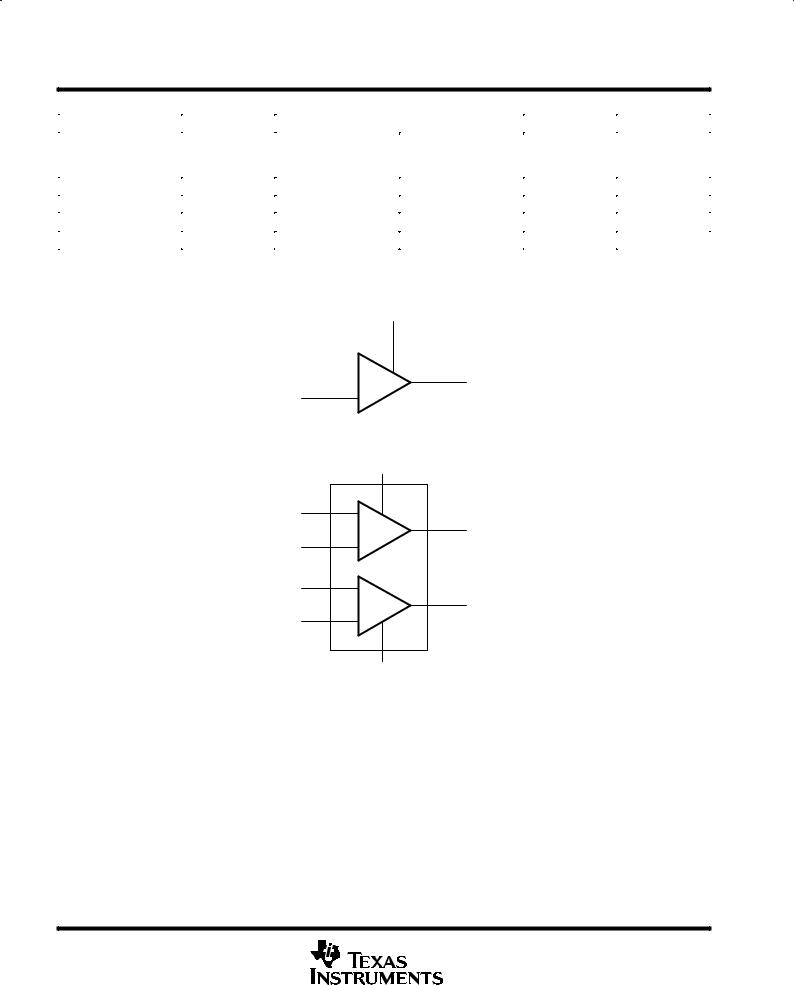
functional block diagram
|
|
|
Null |
|
2 |
|
1 |
IN± |
|
8 |
|
|
|
||
|
|
|
6
OUT
3
IN+
Figure 2. THS4021 ± Single Channel
VCC
1IN±
1OUT
1IN+
2IN±
2OUT
2IN+
±VCC
Figure 3. THS4022 ± Dual Channel
2 |
POST OFFICE BOX 655303 •DALLAS, TEXAS 75265 |

THS4021, THS4022
350-MHz LOW-NOISE HIGH-SPEED AMPLIFIERS
SLOS265B ± SEPTEMBER 1999 ± REVISED FEBRUARY 2000
absolute maximum ratings over operating free-air temperature (unless otherwise noted)²
Supply voltage, VCC . . . . . . . . . . . . . . . . . . . . . . . . . . . . . . . . . . . . . . . . . . . . . . . . . . |
. . . . . . . . . . . . . . . . . . ±16.5 V |
Input voltage, VI . . . . . . . . . . . . . . . . . . . . . . . . . . . . . . . . . . . . . . . . . . . . . . . . . . . . . . |
. . . . . . . . . . . . . . . . . . . . ±VCC |
Output current, IO . . . . . . . . . . . . . . . . . . . . . . . . . . . . . . . . . . . . . . . . . . . . . . . . . . . . . |
. . . . . . . . . . . . . . . . . . 150 mA |
Differential input voltage, VIO . . . . . . . . . . . . . . . . . . . . . . . . . . . . . . . . . . . . . . . . . . . |
. . . . . . . . . . . . . . . . . . . . . ± 4 V |
Continuous total power dissipation . . . . . . . . . . . . . . . . . . . . . . . . . . . . . . . . . . . . . |
See Dissipation Rating Table |
Maximum junction temperature, TJ . . . . . . . . . . . . . . . . . . . . . . . . . . . . . . . . . . . . . |
. . . . . . . . . . . . . . . . . . . 150°C |
Operating free-air temperature, TA: C-suffix . . . . . . . . . . . . . . . . . . . . . . . . . . . . . |
. . . . . . . . . . . . . . 0°C to 70°C |
I-suffix . . . . . . . . . . . . . . . . . . . . . . . . . . . . . . |
. . . . . . . . . . . . ±40°C to 85°C |
Storage temperature, Tstg . . . . . . . . . . . . . . . . . . . . . . . . . . . . . . . . . . . . . . . . . . . . . . |
. . . . . . . . . . . ±65°C to 150°C |
Lead temperature 1,6 mm (1/16 inch) from case for 10 seconds . . . . . . . . . . . . |
. . . . . . . . . . . . . . . . . . . 300°C |
²Stresses beyond those listed under ªabsolute maximum ratingsº may cause permanent damage to the device. These are stress ratings only and functional operation of the device at these or any other conditions beyond those indicated under ªrecommended operating conditionsº is not implied. Exposure to absolute-maximum-rated conditions for extended periods may affect device reliability.
DISSIPATION RATING TABLE
PACKAGE |
θJA |
θJC |
TA = 25°C |
|
(°C/W) |
(°C/W) |
POWER RATING |
||
|
||||
|
|
|
|
|
D |
167³ |
38.3 |
740 mW |
|
DGN§ |
58.4 |
4.7 |
2.14 W |
³ This data was taken using the JEDEC standard Low-K test PCB. For the JEDEC Proposed High-K test PCB, the θJA is 95°C/W with a power rating at TA = 25°C of 1.32 W.
§ This data was taken using 2 oz. trace and copper pad that is soldered directly to a 3 in. × 3 in. PC. For further information, refer to Application Information section of this data sheet.
recommended operating conditions
|
|
MIN NOM |
MAX |
UNIT |
|
|
|
|
|
|
|
Supply voltage, VCC+ and VCC ± |
Dual supply |
± 4.5 |
±16 |
V |
|
|
|
|
|||
Single supply |
9 |
32 |
|||
|
|
||||
|
|
|
|
|
|
Operating free-air temperature, TA |
C-suffix |
0 |
70 |
°C |
|
|
|
|
|||
I-suffix |
± 40 |
85 |
|||
|
|
POST OFFICE BOX 655303 •DALLAS, TEXAS 75265 |
3 |
THS4021, THS4022
350-MHz LOW-NOISE HIGH-SPEED AMPLIFIERS
SLOS265B ± SEPTEMBER 1999 ± REVISED FEBRUARY 2000
electrical characteristics at TA = 25°C, VCC = ±15 V, RL = 150 Ω (unless otherwise noted)
dynamic performance
|
PARAMETER |
|
TEST CONDITIONS |
|
MIN |
TYP |
MAX |
UNIT |
|||
|
|
|
|
|
|
|
|
|
|
|
|
|
|
VCC = ± 15 V |
|
Gain = 10 |
|
350 |
|
MHz |
|||
|
Small-signal bandwidth (±3 dB) |
VCC = ± 5 V |
|
|
280 |
|
|||||
|
|
|
|
|
|
|
|
||||
|
VCC = |
± 15 V |
|
Gain = 20 |
|
80 |
|
MHz |
|||
|
|
|
|
|
|||||||
BW |
|
VCC = ± 5 V |
|
|
70 |
|
|||||
|
|
|
|
|
|
|
|
||||
Bandwidth for 0.1 dB flatness |
VCC = |
± 15 V |
|
Gain = 10 |
|
17 |
|
MHz |
|||
|
|
|
|
||||||||
|
VCC = |
± 5 V |
|
|
17 |
|
|||||
|
|
|
|
|
|
|
|
|
|||
|
Full power bandwidth² |
VO(pp) = 20 V, |
VCC = ± 15 V |
|
|
3.7 |
|
MHz |
|||
|
VO(pp) = 5 V, |
VCC = ± 5 V |
|
|
11.8 |
|
|||||
|
|
|
|
|
|
|
|
||||
SR |
Slew rate³ |
VCC = ± 15 V, |
10-V step, |
Gain = 10 |
|
470 |
|
V/µs |
|||
VCC = ± 5 V, |
5-V step |
|
370 |
|
|||||||
|
|
|
|
|
|
|
|
||||
|
Settling time to 0.1% |
VCC = ± 15 V, |
5-V step |
Gain = ±10 |
|
40 |
|
ns |
|||
ts |
VCC = |
± 5 V, |
2-V step |
|
50 |
|
|||||
|
|
|
|
|
|
|
|||||
Settling time to 0.01% |
VCC = |
± 15 V, |
5-V step |
Gain = ±10 |
|
145 |
|
ns |
|||
|
|
|
|||||||||
|
VCC = |
± 5 V, |
2-V step |
|
150 |
|
|||||
|
|
|
|
|
|
|
|
||||
² Slew rate is measured from an output level range of 25% to 75%. |
|
|
|
|
|
|
|
|
|||
³ Full power bandwidth = slew rate / 2π VO(Peak). |
|
|
|
|
|
|
|
|
|
||
noise/distortion performance |
|
|
|
|
|
|
|
|
|
|
|
|
|
|
|
|
|
|
|
|
|
|
|
|
PARAMETER |
|
TEST CONDITIONS |
|
MIN |
TYP |
MAX |
UNIT |
|||
|
|
|
|
|
|
|
|
|
|
|
|
|
|
|
|
VCC = ± 15 V |
RL = 150 Ω |
|
± 68 |
|
|
|
|
|
|
V |
= 2 V, |
RL = 1 kΩ |
|
± 77 |
|
|
|
|
|
|
|
|
|
|
|
|
|
||||
THD |
Total harmonic distortion |
O(pp) |
|
|
|
|
|
|
dBc |
||
f = 1 MHz, Gain = 2 |
VCC = ± 5 V |
RL = 150 Ω |
|
± 69 |
|
||||||
|
|
|
|
|
|
|
|||||
|
|
|
|
RL = 1 kΩ |
|
± 78 |
|
|
|
|
|
|
|
|
|
|
|
|
|
|
|
||
|
|
|
|
|
|
|
|
|
|||
Vn |
Input voltage noise |
VCC = ± 5 V or ± 15 V, |
f = 10 kHz |
|
|
1.5 |
|
nV/√ |
Hz |
|
|
In |
Input current noise |
VCC = ± 5 V or ± 15 V, |
f = 10 kHz |
|
|
2 |
|
pA/√ |
|
|
|
|
|
|
Hz |
|
|||||||
|
Differential gain error |
Gain = 2, |
NTSC, |
VCC = ± 15 V |
|
0.02% |
|
|
|
|
|
|
40 IRE modulation, |
± 100 IRE ramp |
VCC = ± 5 V |
|
|
|
|
|
|||
|
|
|
|
|
|
|
|
||||
|
Differential phase error |
Gain = 2, |
NTSC, |
VCC = ± 15 V |
|
0.08° |
|
|
|
|
|
|
40 IRE modulation, |
± 100 IRE ramp |
VCC = ± 5 V |
|
0.06° |
|
|
|
|
||
|
|
|
|
|
|
|
|||||
XT |
Channel-to-channel crosstalk |
VCC = |
± 5 V or ± 15 V, |
f = 1 MHz |
|
|
± 60 |
|
dB |
||
(THS4022 only) |
|
|
|
||||||||
|
|
|
|
|
|
|
|
|
|
|
|
4 |
POST OFFICE BOX 655303 •DALLAS, TEXAS 75265 |
THS4021, THS4022
350-MHz LOW-NOISE HIGH-SPEED AMPLIFIERS
SLOS265B ± SEPTEMBER 1999 ± REVISED FEBRUARY 2000
electrical characteristics at TA = 25°C, VCC = ±15 V, RL = 150 Ω (unless otherwise noted) (continued)
dc performance
|
PARAMETER |
|
|
TEST CONDITIONS |
|
MIN |
TYP |
MAX |
UNIT |
|||
|
|
|
|
|
|
|
|
|
|
|
|
|
|
|
V |
CC |
= ± 15 V, |
V |
O |
= ± 10 V, |
TA = 25°C |
40 |
60 |
|
V/mV |
|
|
RL = 1 kΩ |
|
|
|
T = full range |
35 |
|
|
|||
|
|
|
|
|
|
|
|
|||||
|
Open loop gain |
|
|
|
|
|
|
A |
|
|
|
|
|
V |
CC |
= ± 5 V, |
V |
O |
= ± 2.5 V, |
TA = 25°C |
20 |
35 |
|
V/mV |
|
|
|
|
||||||||||
|
|
RL = 250 Ω |
|
|
|
T = full range |
15 |
|
|
|||
|
|
|
|
|
|
|
|
|||||
|
|
|
|
|
|
|
|
A |
|
|
|
|
VOS |
Input offset voltage |
|
|
|
|
|
|
TA = 25°C |
|
0.5 |
2 |
mV |
|
|
|
|
|
|
TA = full range |
|
|
3 |
|||
|
|
|
|
|
|
|
|
|
|
|
||
|
Offset voltage drift |
|
|
|
|
|
|
TA = full range |
|
15 |
|
µV/°C |
IIB |
Input bias current |
VCC = ± 5 V or ± 15 V |
|
|
|
TA = 25°C |
|
3 |
6 |
µA |
||
|
|
|
|
|
|
TA = full range |
|
|
6 |
|||
|
|
|
|
|
|
|
|
|
|
|
||
IOS |
Input offset current |
|
|
|
|
|
|
TA = 25°C |
|
30 |
250 |
nA |
|
|
|
|
|
|
TA = full range |
|
|
400 |
|||
|
|
|
|
|
|
|
|
|
|
|
||
|
Offset current drift |
TA = full range |
|
|
|
|
|
0.3 |
|
nA/°C |
||
input characteristics
|
PARAMETER |
|
TEST CONDITIONS |
MIN |
TYP MAX |
UNIT |
|
|
|
|
|
|
|
VICR |
Common-mode input voltage range |
VCC = ± 15 V |
|
±13.8 |
±14.3 |
V |
VCC = ± 5 V |
|
± 3.8 |
± 4.3 |
|||
|
|
|
|
|||
CMRR |
Common mode rejection ratio |
VCC = ± 15 V, |
VICR = ± 12 V, TA = full range |
74 |
95 |
dB |
ri |
Input resistance |
|
|
|
1 |
MΩ |
Ci |
Input capacitance |
|
|
|
1.5 |
pF |
output characteristics
|
PARAMETER |
|
TEST CONDITIONS |
MIN |
TYP MAX |
UNIT |
|
|
|
|
|
|
|
|
|
|
|
VCC = ± 15 V |
|
RL = 250 Ω |
±12 |
±12.5 |
V |
VO |
Output voltage swing |
VCC = ± 5 V |
|
RL = 150 Ω |
± 3 |
± 3.3 |
|
|
|
||||||
VCC = ± 15 V |
|
RL = 1 kΩ |
±13 |
±13.5 |
V |
||
|
|
|
|||||
|
|
VCC = ± 5 V |
|
± 3.4 |
± 3.8 |
||
|
|
|
|
|
|||
IO |
Output current |
VCC = ± 15 V |
|
RL = 20 Ω |
80 |
100 |
mA |
VCC = ± 5 V |
|
50 |
75 |
||||
|
|
|
|
|
|||
I |
Short-circuit current² |
V = ± 15 V |
|
|
|
150 |
mA |
SC |
|
CC |
|
|
|
|
|
RO |
Output resistance² |
Open loop |
|
|
|
13 |
Ω |
²Observe power dissipation ratings to keep the junction temperature below the absolute maximum rating when the output is heavily loaded or shorted. See the absolute maximum ratings section of this data sheet for more information.
power supply
|
PARAMETER |
TEST CONDITIONS |
|
MIN |
TYP |
MAX |
UNIT |
|
|
|
|
|
|
|
|
|
|
VCC |
Supply voltage operating range |
Dual supply |
|
± 4.5 |
|
±16.5 |
V |
|
|
|
|
|
|
|
|||
Single supply |
|
9 |
|
33 |
|
|||
|
|
|
|
|
|
|||
|
|
|
|
|
|
|
|
|
|
|
VCC = ± 15 V |
TA = 25°C |
|
7.8 |
10 |
|
|
ICC |
Supply current (per amplifier) |
TA = full range |
|
|
11 |
mA |
|
|
|
|
|
|
|||||
VCC = ± 5 V |
TA = 25°C |
|
6.7 |
9 |
|
|||
|
|
|
|
|
||||
|
|
TA = full range |
|
|
10.5 |
|
|
|
|
|
|
|
|
|
|
||
PSRR |
Power supply rejection ratio |
VCC = ± 5 V or ± 15 V |
TA = full range |
80 |
95 |
|
dB |
|
|
|
|
|
|
|
|
|
|
|
|
|
|
|
|
|
|
|
POST OFFICE BOX 655303 •DALLAS, TEXAS 75265 |
5 |

THS4021, THS4022
350-MHz LOW-NOISE HIGH-SPEED AMPLIFIERS
SLOS265B ± SEPTEMBER 1999 ± REVISED FEBRUARY 2000
TYPICAL CHARACTERISTICS
OPEN LOOP GAIN AND
|
|
CROSSTALK |
|
|
|
|
|
vs |
|
|
|
FREQUENCY |
|
|
|
10 |
|
|
|
|
0 |
VCC = ± 15 V |
|
|
|
Gain = 10 |
|
|
|
|
|
|
|
|
|
±10 |
RF = 220 Ω |
|
|
|
±20 |
RL = 150 Ω |
|
|
± dB |
|
|
|
|
±30 |
|
|
|
|
Crosstalk |
|
|
|
|
±40 |
|
|
|
|
±50 |
|
|
|
|
|
±60 |
|
|
|
|
±70 |
|
|
|
|
±80 |
|
|
|
|
1 M |
10 M |
100 M |
1 G |
|
|
f ± Frequency ± Hz |
|
|
Figure 4
PHASE RESPONSE
|
|
|
vs |
|
|
|
|
|
120 |
|
FREQUENCY |
|
30 |
|
|
|
|
|
|
|
|
||
|
|
VCC = ± 5 V & ±15 V |
|
|
|
|
|
|
100 |
|
|
|
|
0 |
|
|
|
|
Gain |
|
|
|
|
dB |
80 |
|
|
|
|
±30 |
|
± |
|
|
|
|
|
|
|
Loop Gain |
60 |
|
|
|
|
±60 |
Phase |
40 |
Phase |
|
|
|
±90 |
||
|
|
|
|
||||
|
|
|
|
|
|
||
Open |
20 |
|
|
|
|
±120 |
|
|
|
|
|
|
|
|
|
|
0 |
|
|
|
|
±150 |
|
|
±20 |
|
|
|
|
±180 |
|
|
1 k |
10 k |
100 k 1 M |
10 M |
100 M |
1 G |
|
|
|
|
f ± Frequency ± Hz |
|
|
|
|
Figure 5
TOTAL HARMONIC DISTORTION |
DISTORTION |
DISTORTION |
vs |
vs |
vs |
FREQUENCY |
OUTPUT VOLTAGE |
OUTPUT VOLTAGE |
THD ± Total Harmonic Distortion ± dBc
±40 |
|
|
|
±10 |
VCC = ± 15 V |
|
|
|
±10 |
|
|
|
|
|
|
|
|
||
|
VCC = ± 15 V |
|
|
|
|
|
|
|
|
|
|
|
|
RL = 1 kΩ |
|
|
|
|
|
±50 |
Gain = 10 |
|
|
±30 |
G = 10 |
|
|
|
±30 |
VO(PP) = 2 V |
|
|
f = 1 MHz |
|
|
|
|||
|
|
dBc |
|
|
|
dBc± |
|
||
±60 |
|
|
±50 |
|
|
|
±50 |
||
|
|
|
|
|
|
|
|||
|
RL = 150 Ω |
|
|
|
|
|
|
||
±70 |
|
Distortion± |
|
|
2nd Harmonic |
Distortion |
|
||
|
|
|
|
|
|||||
|
|
|
|
|
|
|
|
|
|
|
|
|
|
±70 |
|
|
|
|
±70 |
±80 |
RL = 1 kΩ |
|
|
|
|
|
|
|
|
±90 |
|
|
|
±90 |
|
|
|
|
±90 |
|
|
|
|
|
|
3rd Harmonic |
|
|
|
|
|
|
|
|
|
|
|
|
|
±100 |
|
|
|
±110 |
|
|
|
|
±110 |
|
|
|
0 |
5 |
10 |
15 |
20 |
|
|
100 k |
1 M |
10 M |
|
|
|||||
|
f ± Frequency ± Hz |
|
|
|
VO ± Output Voltage ± V |
|
|
||
|
VCC = ± 15 V |
|
|
|
|
RL = 150 Ω |
|
|
|
|
G = 10 |
|
|
|
|
f = 1 MHz |
|
|
|
|
2nd Harmonic |
|
|
|
|
|
|
3rd Harmonic |
|
0 |
5 |
10 |
15 |
20 |
|
VO ± Output Voltage ± V |
|
||
Figure 6 |
Figure 7 |
Figure 8 |
|
|
|
DISTORTION |
|
|
|
DISTORTION |
|
|
|
|
DISTORTION |
|
|
|
|
|
vs |
|
|
|
|
vs |
|
|
|
|
vs |
|
|
|
|
FREQUENCY |
|
|
|
FREQUENCY |
|
|
|
|
FREQUENCY |
|
|
|
±50 |
VCC = ± 15 V |
|
|
±50 |
VCC = ± 5 V |
|
|
|
±50 |
VCC = ± 15 V |
|
||
|
|
|
|
|
|
|
|
|
|
|||||
|
|
RL = 1 kΩ |
|
|
|
|
RL = 1 kΩ |
|
|
|
|
RL = 150 Ω |
|
|
|
±60 |
G = 10 |
|
|
|
±60 |
G = 10 |
|
|
|
±60 |
G = 10 |
|
|
|
VO(PP) = 2 V |
|
|
VO(PP) = 2 V |
2nd Harmonic |
|
|
VO(PP) = 2 V |
|
|||||
|
|
|
|
|
|
|
|
|
||||||
dBc |
|
|
|
|
dBc |
|
|
|
|
dBc |
±70 |
|
2nd Harmonic |
|
±70 |
|
|
|
±70 |
|
|
|
|
|
|
||||
± |
|
|
|
± |
|
|
|
± |
|
|
|
|||
|
|
|
|
|
|
|
|
|
|
|
|
|||
Distortion |
|
2nd Harmonic |
|
Distortion |
|
|
|
|
Distortion |
|
|
|
|
|
±80 |
|
|
|
±80 |
|
|
|
±80 |
|
|
|
|||
|
|
|
|
|
|
|
|
|
|
3rd Harmonic |
|
|||
|
|
|
|
|
|
|
|
|
|
|
|
|
|
|
|
±90 |
|
3rd Harmonic |
|
|
±90 |
|
|
|
|
±90 |
|
|
|
|
|
|
|
|
|
3rd Harmonic |
|
|
|
|
|
|||
|
|
|
|
|
|
|
|
|
|
|
|
|
|
|
±100 |
|
|
|
|
±100 |
|
|
|
|
±100 |
|
|
|
|
|
100 k |
1 M |
10 M |
|
100 k |
1 M |
10 M |
|
100 k |
1 M |
10 M |
|||
|
|
|
f ± Frequency ± Hz |
|
|
|
f ± Frequency ± Hz |
|
|
|
|
f ± Frequency ± Hz |
|
|
|
|
|
Figure 9 |
|
|
|
Figure 10 |
|
|
|
|
Figure 11 |
|
|
6 |
POST OFFICE BOX 655303 •DALLAS, TEXAS 75265 |
THS4021, THS4022
350-MHz LOW-NOISE HIGH-SPEED AMPLIFIERS
SLOS265B ± SEPTEMBER 1999 ± REVISED FEBRUARY 2000
TYPICAL CHARACTERISTICS
|
|
|
DISTORTION |
|
|
|
|
vs |
|
|
|
|
FREQUENCY |
|
|
±40 |
VCC = ± 5 V |
|
|
|
|
|
||
|
±50 |
RL = 150 Ω |
|
|
|
G = 10 |
2nd Harmonic |
|
|
|
|
VO(PP) = 2 V |
|
|
± dBc |
±60 |
|
|
|
|
|
|
|
|
Distortion |
±70 |
|
|
|
±80 |
|
3rd Harmonic |
|
|
|
|
|
||
|
±90 |
|
|
|
|
±100 |
|
|
|
|
100 k |
|
1 M |
10 M |
|
|
|
f ± Frequency ± Hz |
|
OUTPUT AMPLITUDE
|
|
|
|
vs |
|
|
|
|
|
FREQUENCY |
|
|
|
|
25 |
|
|
|
|
|
± dB |
|
|
|
RF = 220 Ω |
|
|
20 |
|
|
|
|
|
|
Amplitude |
|
|
|
RF = 150 Ω |
|
|
|
|
|
|
|
|
|
Output |
15 |
VCC = ± 15 V |
|
|
|
|
|
|
|
|
|||
|
|
Gain = 10 |
|
|
|
|
|
|
RL = 150 Ω |
|
|
|
|
|
10 |
VO(PP) = 400 mV |
|
|
|
|
|
|
|
|
|
|
|
|
10 k |
100 k |
1 M |
10 M |
100 M |
1 G |
|
|
|
f ± Frequency ± Hz |
|
||
OUTPUT AMPLITUDE
|
|
|
|
vs |
|
|
|
|
|
FREQUENCY |
|
|
|
|
25 |
|
|
|
|
|
± dB |
|
|
|
RF = 220 Ω |
|
|
20 |
|
|
|
|
|
|
Amplitude |
|
|
|
RF = 150 Ω |
|
|
|
|
|
|
|
|
|
Output |
15 |
VCC = ± 5 V |
|
|
|
|
|
|
|
|
|||
|
|
Gain = 10 |
|
|
|
|
|
|
RL = 150 Ω |
|
|
|
|
|
10 |
VO(PP) = 400 mV |
|
|
|
|
|
|
|
|
|
|
|
|
10 k |
100 k |
1 M |
10 M |
100 M |
1 G |
|
|
|
f ± Frequency ± Hz |
|
||
Figure 12 |
Figure 13 |
Figure 14 |
|
|
OUTPUT AMPLITUDE |
|
|
|
OUTPUT AMPLITUDE |
|
|
|
|
|
|
|
|
|
|
|
|
|
|
|||||||||||
|
|
|
|
|
|
vs |
|
|
|
|
|
|
|
|
vs |
|
|
|
|
|
|
|
|
|
|
|
|
|
|
|
|
|
|
|
|
FREQUENCY |
|
|
|
|
FREQUENCY |
|
|
|
|
|
|
|
1-V STEP RESPONSE |
|
|||||||||||||
|
30 |
|
|
|
|
|
|
|
|
|
30 |
|
|
|
|
|
|
|
|
|
00.80. |
|
|
|
|
|
|
|
|
|
|
|
|
|
|
|
|
|
RF = 6.2 kΩ |
|
|
|
|
|
RF = 6.2 kΩ |
|
|
|
|
0.60 |
|
|
|
|
|
|
|
|
|
|
|||
|
|
|
|
|
|
|
|
|
|
|
|
|
|
|
|
|
|
|
|
|
0.6 |
|
|
|
|
|
|
|
|
|
|
dB |
25 |
|
|
|
|
|
|
|
|
dB |
25 |
|
RF = 220 Ω |
|
|
|
|
± V |
0.40 |
|
|
|
|
|
|
|
|
|
|
||
|
|
|
|
|
|
|
|
|
|
|
|
|
|
|
|
|
|
0.4 |
|
|
|
|
|
|
|
|
|
|
|||
Amplitude± |
|
|
|
|
RF = 220 Ω |
|
|
Amplitude± |
|
|
|
|
|
|
|
|
|
VoltageOutput |
|
|
|
|
|
|
|
|
|
|
|
||
|
|
|
|
|
|
|
|
|
|
|
|
|
|
|
|
|
|
|
|
|
|
|
|
|
|
|
|
|
|||
|
|
|
|
|
|
|
|
|
|
|
|
|
|
|
|
|
|
|
|
|
0.20 |
|
|
|
|
|
|
|
|
|
|
|
|
|
|
|
|
|
|
|
|
|
|
|
|
|
|
|
|
|
|
|
0.2 |
|
|
|
|
|
|
|
|
|
|
|
20 |
|
|
|
|
|
|
|
|
|
20 |
|
|
|
|
|
|
|
|
|
|
|
|
|
|
|
|
|
|
|
|
Output |
|
|
|
|
|
|
|
|
|
Output |
|
|
|
|
|
|
|
|
|
|
±0.00 |
|
|
|
|
|
|
|
|
|
|
|
Gain = 20 |
|
RF = 1 kΩ |
|
|
Gain = 20 |
|
RF = 1 kΩ |
|
|
V |
|
|
VCC = ± 5 V |
|
|
|
|
|
||||||||||||
|
|
|
|
|
|
|
|
|
|
|
|
|
|
|
|
|
|
|
|
± |
±0.20 |
|
|
|
|
|
|
||||
|
15 |
VCC = ±15 V |
|
|
|
|
|
15 VCC = ±5 V |
|
|
|
|
|
|
O |
±0.2 |
|
Gain = 10 |
|
|
|
|
|
||||||||
|
|
|
|
|
|
|
|
|
|
|
|
|
|
|
|
|
|
|
|||||||||||||
|
|
|
|
|
|
|
|
|
|
|
|
|
|
|
|
|
|
|
|
|
±0.40 |
|
RF = 220 Ω |
|
|
|
|
|
|||
|
|
RL = 150 Ω |
|
|
|
|
|
|
RL = 150 Ω |
|
|
|
|
|
|
|
±0.4 |
|
RL = 150 Ω |
|
|
|
|
|
|||||||
|
10 |
VO(PP) = 400 mV |
|
|
|
|
10 |
VO(PP) = 400 mV |
|
|
|
|
|
±0.60 |
|
|
|
|
|
|
|
|
|
|
|||||||
|
|
|
10 |
|
|
|
|
|
|
100 k |
|
1 M |
|
100M |
|
1000M |
10000G |
|
±0.6 |
|
|
|
|
|
|
|
|
|
|
||
|
100 k |
1 M |
|
100M |
|
1000M |
|
10000G |
|
|
10 |
|
|
|
|
|
|
|
0 |
|
50 |
100 |
150 |
200 |
250 |
300 |
350 |
400 |
|||
|
|
|
|
|
|
f ± Frequency ± Hz |
|
|
|
|
|
|
|
|
t ± Time ± ns |
|
|
|
|||||||||||||
|
|
|
|
f ± Frequency ± Hz |
|
|
|
|
|
|
|
|
|
|
|
|
|
|
|
||||||||||||
|
|
|
|
|
Figure 15 |
|
|
|
|
|
Figure 16 |
|
|
|
|
|
|
|
|
|
Figure 17 |
|
|
|
|
||||||
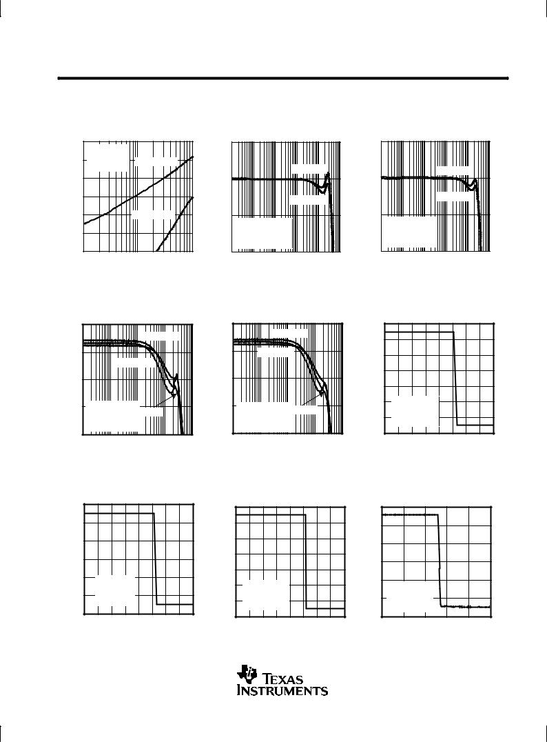
|
|
5-V STEP RESPONSE |
|
|
|
1-V STEP RESPONSE |
|
|
|
|
10-V STEP RESPONSE |
|
|||||||||||||||||||
|
3 |
|
|
|
|
|
|
|
|
|
|
|
|
|
|
|
|
||||||||||||||
|
|
|
|
|
|
|
|
|
|
00.80. |
|
|
|
|
|
|
|
|
|
6 |
|
|
|
|
|
|
|
|
|
|
|
|
|
|
|
|
|
|
|
|
|
|
|
|
|
|
|
|
|
|
|
|
|
|
|
|
|
|
|
|
|
||
|
2 |
|
|
|
|
|
|
|
|
|
00.60. |
|
|
|
|
|
|
|
|
|
4 |
|
|
|
|
|
|
|
|
|
|
|
|
|
|
|
|
|
|
|
|
|
|
|
|
|
|
|
|
|
|
|
|
|
|
|
|
|
|
|
|
|
|
VoltageOutput± ± V |
1 |
|
|
|
|
|
|
|
|
VoltageOutput± ± V |
0.40 |
|
|
|
|
|
|
|
|
VoltageOutput± ± V |
|
|
|
|
|
|
|
|
|
|
|
|
|
|
|
|
|
|
|
0.4 |
|
|
|
|
|
|
|
|
2 |
|
|
|
|
|
|
|
|
|
|
||||
|
|
|
|
|
|
|
|
|
|
|
|
|
|
|
|
|
|
|
|
|
|
|
|
|
|
|
|
||||
|
|
|
|
|
|
|
|
|
|
|
0. |
|
|
|
|
|
|
|
|
|
|
|
|
|
|
|
|
|
|
|
|
|
0 |
|
|
|
|
|
|
|
|
|
0.20 |
|
|
|
|
|
|
|
|
|
|
|
|
|
|
|
|
|
|
|
|
|
|
|
|
|
|
|
|
|
|
|
|
|
|
|
|
|
|
|
|
0 |
|
|
|
|
|
|
|
|
|
|
|
|
|
|
|
|
|
|
|
|
|
|
|
|
|
|
|
|
|
|
|
|
|
|
|
|
|
|
|
|
|
|
|
|
|
|
|
|
|
|
|
|
|
|
±0.00 |
|
|
|
|
|
|
|
|
|
|
|
|
|
|
|
|
|
|
|
|
|
±1 |
|
|
|
|
|
|
|
|
|
0 |
|
|
|
|
|
|
|
|
|
|
|
|
|
|
|
|
|
|
|
|
|
VCC = ± 5 V |
|
|
|
|
|
|
|
|
|
|
|
|
|
|
|
±2 |
|
|
|
|
|
|
|
|
|
|
||||
O |
|
|
|
|
|
|
±0. |
VCC = ± 15 V |
|
|
|
|
|
|
VCC = ± 15 V |
|
|
|
|
|
|||||||||||
|
Gain = ±10 |
|
|
|
|
O |
|
|
|
|
|
O |
|
|
|
|
|
|
|||||||||||||
|
|
|
|
|
±0.20 |
Gain = 10 |
|
|
|
|
|
|
|
|
|
|
|
|
|||||||||||||
V |
±2 |
RF = 220 Ω |
|
|
|
|
V |
|
|
|
|
|
|
|
V |
|
Gain = 10 |
|
|
|
|
|
|
||||||||
|
|
|
|
|
|
|
RF = 220 Ω |
|
|
|
|
|
|
±4 |
|
|
|
|
|
|
|||||||||||
|
|
R |
L |
= 150 Ω |
|
|
|
|
|
±0.40 |
|
|
|
|
|
|
R |
F |
= 220 Ω |
|
|
|
|
|
|
||||||
|
|
|
|
|
|
|
|
|
|
±0.4 |
RL = 150 Ω |
|
|
|
|
|
|
|
|
|
|
|
|
|
|
|
|
||||
|
±3 |
|
|
|
|
|
|
|
|
|
|
|
|
|
|
|
|
|
RL = 150 |
|
|
|
|
|
|
||||||
|
|
|
|
|
|
|
|
|
|
±0..6 |
|
|
|
|
|
|
|
|
|
±6 |
|
|
|
|
|
|
|
|
|
|
|
|
0 |
50 |
|
100 |
150 |
200 |
250 |
300 |
350 |
400 |
|
|
|
|
|
|
|
|
|
|
|
|
|
|
|
|
|
|
|
||
|
|
0 |
50 |
100 |
150 |
200 |
250 |
300 |
350 |
400 |
|
0 |
|
|
100 |
200 |
300 |
400 |
|
500 |
|||||||||||
|
|
|
|
|
t ± Time ± ns |
|
|
|
|
|
|
|
|||||||||||||||||||
|
|
|
|
|
|
|
|
|
|
|
t ± Time ± ns |
|
|
|
|
|
|
|
|
|
t ± Time ± ns |
|
|
|
|||||||
|
|
|
|
|
|
|
|
|
|
|
|
|
|
|
|
|
|
|
|
|
|
|
|
|
|
||||||
Figure 18 |
Figure 19 |
Figure 20 |
|
|
|
|
|
|
POST OFFICE BOX 655303 •DALLAS, TEXAS 75265 |
7 |
 Loading...