


 Loading...
|
THS3061 |
www.ti.com |
THS3062 |
SLOS394A – JULY 2002 – OCTOBER 2002
LOW DISTORTION, HIGH SLEW RATE CURRENT
FEEDBACK AMPLIFIERS
FEATURES
DUnity Gain Bandwidth: 300 MHz
D0.1 dB Bandwidth: 120 MHz (G=2)
DHigh Slew Rate: 7000 V/µ s
DHD3 at 10 MHz: –81 dBc (G=2, RL = 150 Ω )
DHigh Output Current: ± 145 mA into 50 Ω
DPower Supply Voltage Range: ± 5 V to ± 15 V
APPLICATIONS
DHigh-Speed Signal Processing
DTest and Measurement Systems
DVDSL Line Driver
DHigh-Voltage ADC Preamplifier
DVideo Line Driver
The THS3061 and THS3062 provide well-regulated ac performance characteristics with power supplies ranging from ± 5-V operation up to ± 15-V supplies. Most notable, the 0.1-dB flat bandwidth is exceedingly high, reaching beyond 100 MHz, and the THS306x has less than 0.3 dB of peaking in the frequency response when configured in unity gain. The unity gain bandwidth of 300 MHz allows for excellent distortion characteristics at 10 MHz. The flexibility of the current feedback design allows for a 220-MHz, –3-dB bandwidth in a gain of 10 indicating excellent performance even at high gains.
The THS306x consumes 8.3-mA per channel quiescent current at room temperature and has the capability of producing up to ± 145 mA of output current. The THS3061 is packaged in an 8-pin SOIC and an 8-pin MSOP with PowerPAD . The THS3062 is available in an 8-pin SOIC with PowerPAD and an 8-pin MSP with PowerPAD.
DESCRIPTION
The THS3061 (single) and THS3062 (dual) are high-voltage, high slew-rate current feedback amplifiers utilizing Texas Instruments BICOM-1 process. Designed for low-distortion with a high slew rate of 7000 V/ s, the THS306x amplifiers are ideally suited for applications requiring large, linear output signals such as video line drivers and VDSL line drivers.
RELATED DEVICES AND DESCRIPTIONS
THS3001 Low Distortion Current Feedback Amplifier
THS3112 Dual Current Feedback Amplifier With 175 mA Drive
THS3122 Dual Current Feedback Amplifier With 350 mA Drive
OPA691 Wideband Current Feedback Amplifier With 350 mA
Drive
SLEW RATE vs
OUTPUT STEP
|
8000 |
|
|
|
|
|
|
|
G = 5 |
|
|
|
|
|
7000 |
VCC = ± 15 |
|
|
|
|
s |
6000 |
Rf = 375 Ω |
|
|
|
|
TA = 25° C |
|
|
|
|
||
– V/ |
5000 |
|
|
|
|
|
Rate |
|
|
|
|
|
|
4000 |
|
|
VCC = ± 15 |
|
|
|
Slew |
|
|
|
|
||
3000 |
|
|
|
|
|
|
SR – |
|
|
|
|
|
|
2000 |
|
|
|
|
|
|
|
|
|
|
|
|
|
|
1000 |
|
|
|
|
|
|
0 |
|
|
|
|
|
|
0 |
5 |
10 |
15 |
20 |
25 |
Output Step – VPP
HARMONIC DISTORTION
|
|
|
vs |
|
|
|
|
|
FREQUENCY |
|
|
|
–20 |
|
|
|
|
|
|
G = 1 |
|
|
|
|
–30 |
VCC = ± 15 V |
|
|
|
dB |
–40 |
VCC = ± 5 V |
|
|
|
RL = 1 kΩ |
|
|
|
||
– |
|
|
|
|
|
|
Rf = 750 Ω |
|
|
|
|
Distortion |
–50 |
|
|
|
|
VO = 2VPP |
|
|
|||
–60 |
|
2nd HD |
|
|
|
|
|
|
|
|
|
Harmonic |
–70 |
|
|
|
|
–80 |
|
|
|
|
|
|
|
|
3rd HD |
|
|
|
|
|
|
|
|
|
–90 |
|
|
|
|
|
–100 |
|
|
|
|
|
100 k |
1 M |
10 M |
100 M |
|
|
|
f – Frequency – Hz |
|
||
Please be aware that an important notice concerning availability, standard warranty, and use in critical applications of Texas Instruments semiconductor products and disclaimers thereto appears at the end of this data sheet.
PowerPAD is a trademark of Texas Instruments.
PRODUCTION DATA information is current as of publication date. Products |
Copyright 2002, Texas Instruments Incorporated |
conform to specifications per the terms of Texas Instruments standard warranty. |
|
Production processing does not necessarily include testing of all parameters. |
|
THS3061
THS3062 |
|
|
|
|
|
|
|
|
|
|
|
|
|
|
|
|
|
|
|
www.ti.com |
||||
SLOS394A – JULY 2002 – OCTOBER 2002 |
|
|
|
|
|
|
|
|
|
|
|
|
|
|
|
|
|
|
|
|
|
|
|
|
ABSOLUTE MAXIMUM RATINGS |
|
|
|
|
|
|
This integrated circuit can be damaged by ESD. Texas |
|||||||||||||||||
|
|
|
|
|
|
Instruments recommends that all integrated circuits be |
||||||||||||||||||
over operating free-air temperature range unless otherwise noted(1) |
|
|
|
|||||||||||||||||||||
|
|
|
handled with appropriate precautions. Failure to observe |
|||||||||||||||||||||
|
|
|
|
|
|
|
|
|
|
|||||||||||||||
|
|
|
|
UNIT |
|
|
proper handling and installation procedures can cause damage. |
|||||||||||||||||
|
|
|
|
|
|
|
|
ESD damage can range from subtle performance degradation to |
||||||||||||||||
Supply voltage, VS± |
|
|
16.5 V |
|
|
|||||||||||||||||||
|
|
|
|
|
|
|
|
|
complete device failure. Precision integrated circuits may be more |
|||||||||||||||
Input voltage, VI |
|
|
± |
VS |
|
|||||||||||||||||||
|
|
|
|
susceptible to damage because very small parametric changes could |
||||||||||||||||||||
Output current, IO |
|
|
200 mA |
|
|
|||||||||||||||||||
|
|
|
|
cause the device not to meet its published specifications. |
|
|||||||||||||||||||
Differential input voltage, VID |
|
|
± 3 V |
|
|
PACKAGE DISSIPATION RATINGS |
|
|
|
|
||||||||||||||
Continuous power dissipation |
See Dissipation Rating Table |
|
|
|
|
|
|
|||||||||||||||||
Maximum junction temperature, TJ |
|
|
150° C |
|
|
|
|
|
|
θ JC |
θ JA |
|
|
POWER RATING |
||||||||||
|
|
|
|
|
|
|
|
|
PACKAGE |
|
|
|
(T |
|
= 125° C) |
|
||||||||
|
|
|
|
|
|
|
|
|
|
|
|
|||||||||||||
Operating free-air temperature range, TA |
|
–40° C to 85° C |
|
|
|
(° C/W) |
(° C/W) |
|
|
J |
|
|
|
|
||||||||||
|
|
|
|
|
|
|
|
TA ≤ 25° C |
TA = 85° C |
|||||||||||||||
Storage temperature range, Tstg |
|
|
–65° C to 150° C |
|
|
|
|
|
|
|
|
|
|
|
||||||||||
|
|
|
|
D(8 pin)(1) |
|
38.3 |
|
95 |
|
|
|
1.05 W |
|
|
0.42 W |
|||||||||
Lead temperature |
|
|
300° C |
|
|
|
|
|
|
|
|
|
||||||||||||
|
|
|
|
DDA (8 pin) |
|
9.2 |
|
45.8 |
|
|
|
2.18 W |
|
|
0.87 W |
|||||||||
1,6 mm (1/16 inch) from case for 10 seconds |
|
|
|
|
|
|
|
|
|
|
||||||||||||||
|
|
|
|
|
|
|
|
|
|
|
|
|
||||||||||||
(1) Stresses above these ratings may cause permanent damage. |
|
|
DGN (8 pin)(2) |
|
4.7 |
|
58.4 |
|
|
|
1.71 W |
|
|
0.68 W |
||||||||||
Exposure to absolute maximum conditions for extended periods |
|
|
(1) This data was taken using the JEDEC High-K test PCB. For the |
|||||||||||||||||||||
may degrade device reliability. These are stress ratings only, and |
|
|
JEDEC Low-K test PCB, θ JA is 167° C/W with power rating at |
|||||||||||||||||||||
functional operation of the device at these or any other conditions |
|
|
||||||||||||||||||||||
|
|
TA = 25° C of 0.6 W. |
|
|
|
|
|
|
|
|
|
|
||||||||||||
beyond those specified is not implied. |
|
|
|
|
|
|
|
|
|
|
|
|
|
|
|
|||||||||
|
|
|
|
|
(2) This data was taken using 2 oz. trace and copper pad that is |
|||||||||||||||||||
(2) The THS306x may incorporate a PowerPAD on the underside of |
|
|
soldered directly to a 3 in. x 3 in. PCB. |
|
|
|
|
|
|
|
||||||||||||||
the chip. This acts as a heatsink and must be connected to a |
|
|
|
|
|
|
|
|
|
|||||||||||||||
|
|
|
|
|
|
|
|
|
|
|
|
|
|
|
|
|
|
|||||||
thermally dissipative plane for proper power dissipation. Failure |
|
|
RECOMMENDED OPERATING CONDITIONS |
|||||||||||||||||||||
to do so may result in exceeding the maximum junction |
|
|
||||||||||||||||||||||
|
|
|
|
|
|
|
|
|
|
|
|
|
|
|
|
|
|
|||||||
temperature which could permanently damage the device. See TI |
|
|
|
|
|
|
|
|
|
|
|
|
MIN |
|
MAX |
|
UNIT |
|||||||
technical brief SLMA002 for more information about utilizing the |
|
|
|
|
|
|
|
|
|
|
|
|
|
|
|
|
|
|
||||||
|
|
|
|
|
|
|
Dual supply |
|
|
± 5 |
|
± 15 |
|
|
||||||||||
PowerPAD thermally enhanced package. |
|
|
|
|
|
Supply voltage |
|
|
|
|
|
|
V |
|||||||||||
|
|
|
|
|
|
|
|
|
|
|
|
|
|
|
|
|
||||||||
|
|
|
|
|
|
|
Single supply |
|
10 |
|
30 |
|
||||||||||||
|
|
|
|
|
|
|
|
|
|
|
|
|
|
|||||||||||
|
|
|
|
|
|
|
|
|
|
|
|
|
|
|
|
|
|
|||||||
|
|
|
|
|
|
|
|
|
|
|
|
|
|
|
|
|
|
|
|
|||||
|
|
|
|
|
|
|
|
|
Operating free-air temperature, TA |
|
|
–40 |
|
85 |
|
° C |
||||||||
PACKAGE/ORDERING INFORMATION |
|
|
|
|
|
|
|
|
|
|
|
|
|
|
|
|
|
|
|
|
||||
|
|
|
|
|
|
|
|
|
|
|
|
|
|
|
|
|
||||||||
|
|
|
|
|
|
ORDERABLE PACKAGE AND NUMBER |
|
|
|
|
|
|
|
|
||||||||||
NUMBER OF CHANNELS |
|
|
|
|
|
(OPERATING RANGE FROM –40° C TO 85° C) |
|
|
|
|
|
|
|
|
||||||||||
|
|
|
|
|
|
|
|
|
|
|
|
|
|
|
|
|
|
|
|
|
|
|
|
|
PLASTIC SOIC-8(1) |
|
PLASTIC SOIC-8(1) |
|
PLASTIC MSOP-8(1) |
|
PACKAGE MARKING |
||||||||||||||||||
|
|
|
|
|||||||||||||||||||||
|
|
(D) |
|
|
PowerPAD (DDA) |
|
PowerPAD (DGN) |
|
||||||||||||||||
|
|
|
|
|
|
|
|
|
|
|
|
|
|
|||||||||||
|
|
|
|
|
|
|
|
|
|
|
|
|
|
|
|
|
||||||||
1 |
|
THS3061D |
|
|
|
|
— |
|
|
THS3061DGN |
|
|
|
|
BIB |
|
||||||||
|
|
|
|
|
|
|
|
|
|
|
|
|
|
|
|
|||||||||
2 |
|
THS3062D |
|
|
|
THS3062DDA |
|
|
THS3062DGN |
|
|
|
|
BIC |
|
|||||||||
(1) This package is available taped and reeled. To order this packaging option, add an R suffix to the part number (e.g., THS3062DGNR).
PIN ASSIGNMENTS
TOP VIEW |
|
|
|
|
|
|
|
|
|
|
|
|
|
D, DGN |
TOP VIEW |
|
|
|
|
|
|
|
|
|
|
D, DDA, DGN |
|||
|
|
|
|
THS3061 |
|
|
|
|
|
THS3062 |
|
|
|
||||||||||||||||
|
|
|
|
|
|
|
|
|
|
|
|
|
|
|
|
|
|
|
|
|
|
||||||||
NC |
|
|
1 |
|
|
8 |
|
|
|
NC |
1VOUT |
|
|
|
1 |
|
|
|
8 |
|
|
VS+ |
|||||||
VIN– |
|
|
2 |
|
|
|
|
|
7 |
|
|
|
VS+ |
1VIN– |
|
|
|
2 |
|
|
|
|
|
7 |
|
|
2VOUT |
||
|
|
|
|
|
|
|
|
|
|
|
|
|
|
|
|||||||||||||||
V |
|
|
|
3 |
|
|
|
|
|
6 |
|
|
|
VOUT |
1VIN+ |
|
|
|
|
|
|
|
|
|
|
|
|
|
2VIN– |
|
IN+ |
|
|
|
|
|
|
|
|
|
|
|
|
|
3 |
|
|
|
|
|
|
6 |
|
|
|||||
|
|
|
|
|
|
|
|
|
|
|
|
|
|
|
|
|
|
|
|
|
|
||||||||
VS– |
|
|
4 |
|
|
5 |
|
|
|
NC |
VS– |
|
|
|
4 |
|
|
|
|
|
5 |
|
|
2VIN+ |
|||||
|
|
|
|
|
|
|
|
|
|
|
|
|
|
|
|
||||||||||||||
|
|
|
|
|
|
|
|
|
|||||||||||||||||||||
|
|
|
|
|
|
|
|
|
|
|
|
|
|
|
|
|
|
|
|
|
|
|
|||||||
NC – No internal connection |
|
|
|
|
|
|
|
|
|
|
|
|
|
|
|
|
|||||||||||||
|
|
|
|
|
|
|
|
|
|
|
|
|
|
|
|
||||||||||||||
|
|
|
|
|
|
|
|
|
|
|
|
|
|
|
|
|
|
|
|
|
|
|
|
|
|
|
|
|
|
2

|
|
|
|
|
|
|
|
|
|
THS3061 |
www.ti.com |
|
|
|
|
|
|
|
|
|
THS3062 |
|
|
|
|
|
SLOS394A – JULY 2002 – OCTOBER 2002 |
|||||
ELECTRICAL CHARACTERISTICS |
|
|
|
|
|
|
|
|
||
VS = ± 15 V: Rf = 560 Ω , RL = 150 Ω , and G = +2 unless otherwise noted |
|
|
|
|
|
|
|
|
||
|
|
|
|
|
THS3061, THS3062 |
|
|
|
||
|
|
|
|
|
|
|
|
|
|
|
PARAMETER |
|
TEST CONDITIONS |
TYP |
|
OVER TEMPERATURE |
|
||||
|
|
|
|
|
|
|
|
|
||
|
|
|
25° C |
25° C |
0° C to |
–40° C |
UNITS |
MIN/TYP/ |
||
|
|
|
70° C |
to 85° C |
MAX |
|||||
|
|
|
|
|
|
|
|
|||
|
|
|
|
|
|
|
|
|
|
|
AC PERFORMANCE |
|
|
|
|
|
|
|
|
|
|
|
|
|
|
|
|
|
|
|
|
|
|
G = +1, Rf= 750 Ω |
300 |
|
|
|
|
|
|
|
|
Small-signal bandwidth |
G = +2, Rf = 560 Ω |
275 |
|
|
|
MHz |
Typ |
|||
(VO = 100 mVPP, Peaking < 0.3 dB) |
G = +5, R = 357 Ω |
260 |
|
|
|
|||||
|
|
|
|
|
|
|
||||
|
|
f |
|
|
|
|
|
|
|
|
|
G = +10, Rf = 200 Ω |
220 |
|
|
|
|
|
|
|
|
Bandwidth for 0.1 dB flatness |
G = +2, VO = 100mVpp |
120 |
|
|
|
MHz |
Typ |
|||
Peaking at a gain of +1 |
VO = 100 mVpp |
0.3 |
|
|
|
dB |
Typ |
|||
Large-signal bandwidth |
G = +2, VO = 4 Vpp |
120 |
|
|
|
MHz |
Typ |
|||
Slew rate (25% to 75% level) |
G = +5, 20 V Step |
7000 |
|
|
|
V/µ |
s |
Typ |
||
|
|
|
|
|
|
|||||
G = +2, 10 V Step |
5700 |
|
|
|
||||||
|
|
|
|
|
|
|
|
|||
|
|
|
|
|
|
|
|
|
||
Rise and fall time |
G = +2, VO = 10 V Step |
1 |
|
|
|
ns |
Typ |
|||
Settling time to 0.1% |
G = –2, VO = 2 V Step |
30 |
|
|
|
ns |
Typ |
|||
0.01% |
G = –2, VO = 2 V Step |
125 |
|
|
|
ns |
Typ |
|||
Harmonic distortion |
G = +2, f = 10 MHz, VO = 2 Vpp |
|
|
|
|
|
|
|
|
|
2nd harmonic |
RL = 150 Ω |
–78 |
|
|
|
dBc |
Typ |
|||
RL = 1 kΩ |
–73 |
|
|
|
||||||
3rd harmonic |
RL = 150 Ω |
–81 |
|
|
|
dBc |
Typ |
|||
RL = 1 kΩ |
–82 |
|
|
|
||||||
3rd order intermodulation distortion |
G = +2, fc = 10 MHz, |
|
|
|
|
|
|
|
|
|
V |
= 2 V |
–93 |
|
|
|
dBc |
Typ |
|||
|
O |
pp(envelope) |
|
|
|
|
|
|
|
|
|
∆ f = 200 kHz |
|
|
|
|
|
|
|
|
|
Input voltage noise |
f > 10 kHz |
2.6 |
|
|
|
nV/√ |
Hz |
|
Typ |
|
|
|
|
|
|
|
|
|
|
|
|
Input current noise (noninverting) |
f > 10 kHz |
20 |
|
|
|
pA/√ |
Hz |
|
Typ |
|
|
|
|
|
|
|
|
|
|
||
Input current noise (inverting) |
f > 10 kHz |
36 |
|
|
|
pA/√ |
Hz |
|
Typ |
|
Differential gain (NTSC, PAL) |
G = +2, RL = 150 Ω |
0.02% |
|
|
|
|
|
|
Typ |
|
Differential phase (NTSC, PAL) |
G = +2, RL = 150 Ω |
0.01° |
|
|
|
|
|
|
Typ |
|
DC PERFORMANCE |
|
|
|
|
|
|
|
|
|
|
|
|
|
|
|
|
|
|
|
|
|
Open-loop transimpedance gain |
VO = 0 V, RL = 1 kΩ |
1 |
0.7 |
0.6 |
0.6 |
MΩ |
|
|
Min |
|
Input offset voltage |
VCM = 0 V |
± 0.7 |
± 3.5 |
± 4.4 |
± 4.5 |
mV |
Max |
|||
Average offset voltage drift |
VCM = 0 V |
|
|
± 10 |
± 10 |
µ V/° C |
Typ |
|||
Input bias current (inverting) |
VCM = 0 V |
± 2.0 |
± 20 |
± 32 |
± 35 |
µ A |
Max |
|||
Average bias current drift (–) |
VCM = 0 V |
|
|
± 25 |
± 30 |
nA/° C |
Typ |
|||
Input bias current (noninverting) |
VCM = 0 V |
± 6.0 |
± 25 |
± 38 |
± 40 |
µ A |
Max |
|||
Average bias current drift (+) |
VCM = 0 V |
|
|
± 45 |
± 50 |
nA/° C |
Typ |
|||
INPUT |
|
|
|
|
|
|
|
|
|
|
|
|
|
|
|
|
|
|
|
|
|
Common-mode input range |
|
|
± 13.9 |
± 13.1 |
± 13.1 |
± 13.1 |
V |
|
|
Min |
Common-mode rejection ratio |
VCM = ± 0.5 V |
72 |
60 |
58 |
58 |
dB |
Min |
|||
Input resistance |
Noninverting |
518 |
|
|
|
kΩ |
|
|
Typ |
|
Inverting |
71 |
|
|
|
Ω |
|
|
Typ |
||
|
|
|
|
|
|
|||||
Input capacitance |
Noninverting |
1 |
|
|
|
pF |
Typ |
|||
3

THS3061
THS3062 |
|
|
|
|
|
|
|
|
|
www.ti.com |
|
SLOS394A – JULY 2002 – OCTOBER 2002 |
|
|
|
|
|
|
|
|
|
||
ELECTRICAL CHARACTERISTICS (continued) |
|
|
|
|
|
|
|
|
|
||
VS = ± 15 V: Rf = 560 Ω , RL = 150 Ω |
, and G = +2 unless otherwise noted |
|
|
|
|
|
|
|
|
|
|
|
|
|
|
|
THS3061, THS3062 |
|
|
||||
|
|
|
|
|
|
|
|
|
|
||
PARAMETER |
|
TEST CONDITIONS |
TYP |
|
|
OVER TEMPERATURE |
|||||
|
|
|
|
|
|
|
|
|
|
||
|
|
|
25° C |
25° C |
0° C to |
–40° C |
UNITS |
|
MIN/TYP/ |
||
|
|
|
70° C |
to 85° C |
|
MAX |
|||||
|
|
|
|
|
|
|
|||||
|
|
|
|
|
|
|
|
|
|
|
|
OUTPUT |
|
|
|
|
|
|
|
|
|
|
|
|
|
|
|
|
|
|
|
|
|
|
|
Voltage output swing |
|
RL = 1 kΩ |
± 13.7 |
± 13.4 |
± |
13.4 |
± |
13.3 |
V |
|
Min |
|
RL = 150 Ω |
± 13 |
± 12.6 |
± |
12.4 |
± |
12.3 |
|
|||
|
|
|
|
|
|||||||
Current output, sourcing |
|
RL = 50 Ω |
145 |
140 |
|
135 |
|
130 |
mA |
|
Min |
Current output, sinking |
|
RL = 50 Ω |
–145 |
–140 |
–135 |
–130 |
mA |
|
Min |
||
Closed-loop output impedance |
|
G = +1, f = 1 MHz |
0.1 |
|
|
|
|
|
Ω |
|
Typ |
POWER SUPPLY |
|
|
|
|
|
|
|
|
|
|
|
|
|
|
|
|
|
|
|
|
|
|
|
Specified operating voltage |
|
|
± 15 |
|
|
|
|
|
V |
|
Typ |
|
|
|
|
|
|
|
|
|
|
|
|
Maximum operating voltage |
|
|
|
± 16.5 |
± |
16.5 |
± |
16.5 |
V |
|
Max |
Maximum quiescent current/channel |
|
8.3 |
10 |
11.7 |
|
12 |
mA |
|
Max |
||
|
|
|
|
|
|
|
|
|
|
|
|
Minimum quiescent current/channel |
|
|
8.3 |
6.1 |
|
6 |
|
6 |
mA |
|
Min |
|
|
|
|
|
|
|
|
|
|
|
|
Power supply rejection (+PSRR) |
|
VS+ = 14.50 V to 15.50 V |
76 |
65 |
|
63 |
|
63 |
dB |
|
Min |
Power supply rejection (–PSRR) |
|
VS– = –14.50 V to –15.50 V |
74 |
65 |
|
63 |
|
63 |
dB |
|
Min |
4

|
|
|
|
|
|
|
|
|
|
THS3061 |
www.ti.com |
|
|
|
|
|
|
|
|
|
THS3062 |
|
|
|
|
|
SLOS394A – JULY 2002 – OCTOBER 2002 |
|||||
ELECTRICAL CHARACTERISTICS |
|
|
|
|
|
|
|
|
||
VS = ± 5 V: Rf = 560 Ω , RL = 150 Ω , and G = +2 unless otherwise noted |
|
|
|
|
|
|
|
|
||
|
|
|
|
|
THS3061, THS3062 |
|
|
|||
|
|
|
|
|
|
|
|
|
||
PARAMETER |
|
TEST CONDITIONS |
TYP |
|
OVER TEMPERATURE |
|
||||
|
|
|
|
|
|
|
|
|
||
|
|
|
25° C |
25° C |
0° C to |
–40° C |
UNITS |
MIN/TYP/ |
||
|
|
|
70° C |
to 85° |
C |
MAX |
||||
|
|
|
|
|
|
|
||||
|
|
|
|
|
|
|
|
|
|
|
AC PERFORMANCE |
|
|
|
|
|
|
|
|
|
|
|
|
|
|
|
|
|
|
|
|
|
|
G = +1, Rf= 750 Ω |
275 |
|
|
|
|
|
|
|
|
Small-signal bandwidth |
G = +2, Rf = 560 Ω |
250 |
|
|
|
|
MHz |
Typ |
||
(VO = 100 mVPP, peaking < 0.3 dB) |
G = +5, R = 383 Ω |
230 |
|
|
|
|
||||
|
|
|
|
|
|
|
||||
|
|
f |
|
|
|
|
|
|
|
|
|
G = +10, Rf = 200 Ω |
210 |
|
|
|
|
|
|
|
|
Bandwidth for 0.1 dB flatness |
G = +2, VO = 100 mVpp |
100 |
|
|
|
|
MHz |
Typ |
||
Peaking at a gain of +1 |
VO = 100 mVpp |
< 0.3 |
|
|
|
|
dB |
Typ |
||
Large-signal bandwidth |
G = +2, VO = 4 Vpp |
100 |
|
|
|
|
MHz |
Typ |
||
Slew rate (25% to 75% level) |
G = +1, 5 V Step, Rf= 750 Ω |
2700 |
|
|
|
|
V/µ |
s |
Typ |
|
G = +5, 5 V Step, Rf= 357 Ω |
1300 |
|
|
|
|
|||||
|
|
|
|
|
|
|
|
|||
Rise and fall time |
G = +2, VO = 5 V Step |
2 |
|
|
|
|
ns |
Typ |
||
Settling time to 0.1% |
G = –2, VO = 2 V Step |
20 |
|
|
|
|
ns |
Typ |
||
0.01% |
G = –2, VO = 2 V Step |
160 |
|
|
|
|
||||
|
|
|
|
|
|
|
||||
Harmonic distortion |
G = +2, f = 10 MHz, VO = 2 Vpp |
|
|
|
|
|
|
|
|
|
2nd harmonic |
RL = 150 Ω |
–76 |
|
|
|
|
dBc |
Typ |
||
RL = 1 kΩ |
–70 |
|
|
|
|
|||||
|
|
|
|
|
|
|
|
|||
3rd harmonic |
RL = 150 Ω |
–79 |
|
|
|
|
dBc |
Typ |
||
RL = 1 kΩ |
–77 |
|
|
|
|
|||||
3rd order intermodulation distortion |
G = +2, fc = 10 MHz, |
|
|
|
|
|
|
|
|
|
V |
= 2 V |
–91 |
|
|
|
|
dBc |
Typ |
||
|
O |
pp(envelope) |
|
|
|
|
|
|
|
|
|
∆ f = 200 kHz |
|
|
|
|
|
|
|
|
|
Input voltage noise |
f > 10 kHz |
2.6 |
|
|
|
|
nV/√ |
Hz |
Typ |
|
Input current noise (noninverting) |
f > 10 kHz |
20 |
|
|
|
|
pA/√ |
Hz |
Typ |
|
|
|
|
|
|
|
|
|
|
|
|
Input current noise (inverting) |
f > 10 kHz |
36 |
|
|
|
|
pA/√ |
Hz |
Typ |
|
|
|
|
|
|
|
|
|
|
|
|
Differential gain (NTSC, PAL) |
G = +2, RL = 150 Ω |
0.025% |
|
|
|
|
|
|
Typ |
|
Differential phase (NTSC, PAL) |
G = +2, RL = 150 Ω |
0.01° |
|
|
|
|
|
|
Typ |
|
DC PERFORMANCE |
|
|
|
|
|
|
|
|
|
|
|
|
|
|
|
|
|
|
|
|
|
Open-loop transimpedance gain |
VO = 0 V, RL = 1 kΩ |
0.8 |
0.6 |
0.5 |
0.5 |
|
MΩ |
|
Min |
|
Input offset voltage |
VCM = 0 V |
± 0.3 |
± 3.5 |
± 4.4 |
± 4.5 |
|
mV |
Max |
||
Average offset voltage drift |
VCM = 0 V |
|
|
± 9 |
± 9 |
|
µ V/° C |
Typ |
||
Input bias current (inverting) |
VCM = 0 V |
± 2.0 |
± 20 |
± 32 |
± 35 |
|
µ A |
Max |
||
Average bias current drift (–) |
VCM = 0 V |
|
|
± 20 |
± 25 |
|
nA/° C |
Typ |
||
Input bias current (noninverting) |
VCM = 0 V |
± 6.0 |
± 25 |
± 38 |
± 40 |
|
µ A |
Max |
||
Average bias current drift (+) |
VCM = 0 V |
|
|
± 30 |
± 35 |
|
nA/° C |
Typ |
||
INPUT |
|
|
|
|
|
|
|
|
|
|
|
|
|
|
|
|
|
|
|
|
|
Common-mode input range |
|
|
± 3.9 |
± 3.1 |
± 3.1 |
± 3.1 |
|
V |
|
Min |
|
|
|
|
|
|
|
|
|
||
Common-mode rejection ratio |
VCM = ± 0.5 V |
70 |
60 |
58 |
58 |
|
dB |
Min |
||
Input resistance |
Noninverting |
518 |
|
|
|
|
kΩ |
|
Typ |
|
|
|
|
|
|
|
|
|
|
|
|
Inverting |
71 |
|
|
|
|
Ω |
|
Typ |
||
|
|
|
|
|
|
|||||
Input capacitance |
Noninverting |
1 |
|
|
|
|
pF |
Typ |
||
|
|
|
|
|
|
|
|
|
|
|
5
THS3061
THS3062 |
|
|
|
|
|
|
www.ti.com |
|
SLOS394A – JULY 2002 – OCTOBER 2002 |
|
|
|
|
|
|
|
|
ELECTRICAL CHARACTERISTICS (continued) |
|
|
|
|
|
|
|
|
VS = ± 5 V: Rf = 560 Ω , RL = 150 Ω , and G = +2 unless otherwise noted |
|
|
|
|
|
|
|
|
|
|
|
|
THS3061, THS3062 |
|
|
||
|
|
|
|
|
|
|
|
|
PARAMETER |
TEST CONDITIONS |
TYP |
|
OVER TEMPERATURE |
||||
|
|
|
|
|
|
|
||
|
|
25° C |
25° C |
0° C to |
–40° C |
UNITS |
|
MIN/TYP/ |
|
|
70° C |
to 85° C |
|
MAX |
|||
|
|
|
|
|
|
|||
|
|
|
|
|
|
|
|
|
OUTPUT |
|
|
|
|
|
|
|
|
|
|
|
|
|
|
|
|
|
Voltage output swing |
RL = 1 kΩ |
± 4.1 |
± 3.8 |
± 3.8 |
± 3.7 |
V |
|
Min |
RL = 150 Ω |
± 4.0 |
± 3.6 |
± 3.6 |
± 3.5 |
|
|||
|
|
|
|
|||||
Current output, sourcing |
RL = 50 Ω |
63 |
61 |
60 |
59 |
mA |
|
Min |
Current output, sinking |
RL = 50 Ω |
–63 |
–61 |
–60 |
–59 |
mA |
|
Min |
Closed-loop output impedance |
G = +1, f = 1 MHz |
0.1 |
|
|
|
Ω |
|
Typ |
POWER SUPPLY |
|
|
|
|
|
|
|
|
|
|
|
|
|
|
|
|
|
Specified operating voltage |
|
± 5 |
|
|
|
V |
|
Typ |
Minimum operating voltage |
|
|
± 4.5 |
± 4.5 |
± 4.5 |
V |
|
Min |
|
|
|
|
|
|
|
|
|
Maximum quiescent current |
|
6.3 |
8.0 |
9.2 |
9.5 |
mA |
|
Max |
|
|
|
|
|
|
|
|
|
Minimum quiescent current |
|
6.3 |
5.0 |
4.7 |
4.6 |
mA |
|
Min |
|
|
|
|
|
|
|
|
|
Power supply rejection (+PSRR) |
VS+ = 4.50 V to 5.50 V |
73 |
65 |
63 |
63 |
dB |
|
Min |
Power supply rejection (–PSRR) |
VS– = –4.50 V to –5.50 V |
75 |
65 |
63 |
63 |
dB |
|
Min |
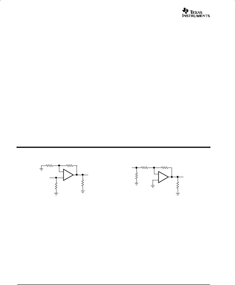
PARAMETER MEASUREMENT INFORMATION
Rg |
|
Rf |
|
Rg |
Rf |
|
_ |
|
|
VI |
|
|
|
|
|
_ |
|
|
|
|
VO |
|
|
VI |
+ |
|
RT |
VO |
|
|
|
|
RL |
|
+ |
|
50 Ω |
|
|
RL |
|
|
|
|
|
Figure 1. Noninverting Test Circuit Figure 2. Inverting Test Circuit
6

|
|
|
|
|
THS3061 |
|
www.ti.com |
|
|
|
THS3062 |
|
|
|
|
SLOS394A – JULY 2002 – OCTOBER 2002 |
|
|
|
TYPICAL CHARACTERISTICS |
|
|
|
Table of Graphs |
|
|
|
|
|
|
|
|
|
|
FIGURE |
|
|
|
|
|
|
|
Small signal frequency response |
|
|
|
3 – 14 |
|
|
|
|
|
|
|
Large signal frequency response |
|
|
|
15, 16 |
|
|
|
|
|
|
|
Harmonic distortion |
|
vs Frequency |
|
17 – 23 |
|
|
|
|
|
|
|
Harmonic distortion |
|
vs Output voltage |
|
24 – 29 |
|
|
|
|
|
|
|
Output impedance |
|
vs Frequency |
|
30 |
|
|
|
|
|
|
|
Common-mode rejection ratio |
|
vs Frequency |
|
31 |
|
|
|
|
|
|
|
Input current noise |
|
vs Frequency |
|
32 |
|
|
|
|
|
|
|
Voltage noise density |
|
vs Frequency |
|
33 |
|
|
|
|
|
|
|
Power supply rejection ratio |
|
vs Frequency |
|
34 |
|
|
|
|
|
|
|
Common-mode rejection ratio (DC) |
|
vs Input common-mode range |
35 |
|
|
|
|
|
|
|
|
Supply current |
|
vs Power supply voltage |
36, 37 |
|
|
|
|
|
|
|
|
Slew rate |
|
vs Output voltage |
|
38, 39 |
|
|
|
|
|
|
|
Slew rate |
|
vs Output step |
|
40 |
|
|
|
|
|
|
|
Input offset voltage |
|
vs Output voltage swing |
41 |
|
|
|
|
|
|
|
|
Overdrive recovery time |
|
|
|
42, 43 |
|
|
|
|
|
|
|
Differential gain |
|
vs Number of 150-Ω |
loads |
44, 45 |
|
|
|
|
|
|
|
Differential phase |
|
vs Number of 150-Ω |
loads |
46, 47 |
7

THS3061
THS3062 |
www.ti.com |
SLOS394A – JULY 2002 – OCTOBER 2002 |
|
|
TYPICAL CHARACTERISTICS |
SMALL SIGNAL FREQUENCY RESPONSE SMALL SIGNAL FREQUENCY RESPONSE SMALL SIGNAL FREQUENCY RESPONSE
|
3 |
|
|
|
|
|
|
3 |
|
|
|
|
|
|
|
2 |
G = 1 |
|
|
|
|
|
|
|
|
|
|
|
|
|
|
|
|
|
|
|
|
|
|
|
|||
|
|
G = 1 |
|
R 500 Ω |
|
|
|
G = 1 |
|
|
|
|
|
|
|
|
Rf 500 |
Ω |
|
||
|
|
|
|
|
|
|
|
R 500 |
Ω |
|
|
|
VCC = ± 15 V |
|
|||||||
|
|
|
|
f |
|
|
|
|
|
|
|
|
|
|
|
|
|
||||
|
2 |
VCC = ± 5 V |
|
|
|
|
2 |
VCC = ± 5 V |
f |
|
|
|
1 |
RL = 150 Ω |
|
|
|
||||
|
|
|
|
|
|
|
|
|
|
|
|
||||||||||
|
1 |
RL = 150 Ω |
|
|
|
|
1 |
RL = 1 kΩ |
|
|
|
|
|
|
VI = 100 mVPP |
|
|
|
|||
|
VI = 100 mVPP |
|
|
|
VI = 100 mVPP |
|
|
|
0 |
|
|
|
|
|
|||||||
|
|
|
|
|
|
|
|
|
|
|
|
|
|
|
|
|
|
|
|
|
|
– dB |
0 |
|
|
|
|
|
– dB |
0 |
|
|
|
|
|
|
– dB |
|
|
|
Rf 1 kΩ |
|
|
|
|
|
|
|
|
|
|
|
|
|
|
|
–1 |
|
|
|
|
||||
Gain |
–1 |
|
|
Rf 1 kΩ |
|
|
Gain |
–1 |
|
|
|
R 1 kΩ |
|
|
Gain |
|
|
|
Rf 750 Ω |
|
|
|
|
|
|
|
|
|
|
|
|
|
|
f |
|
|
|
–2 |
|
|
|
||
|
|
|
|
Rf 750 Ω |
|
|
|
|
|
|
|
|
|
|
|
|
|
|
|
|
|
|
–2 |
|
|
|
|
|
–2 |
|
|
|
Rf 750 Ω |
|
|
|
|
|
|
|
|
||
|
|
|
|
|
|
|
|
|
|
|
|
|
|
–3 |
|
|
|
|
|
||
|
–3 |
|
|
|
|
|
|
–3 |
|
|
|
|
|
|
|
|
|
|
|
|
|
|
|
|
|
|
|
|
|
|
|
|
|
|
|
|
|
|
|
|
|
||
|
–4 |
|
|
|
|
|
|
–4 |
|
|
|
|
|
|
|
–4 |
|
|
|
|
|
|
100 k |
1 M |
10 M |
100M |
1 G |
|
100 k |
1 M |
|
10 M |
100 M |
1 G |
|
100 k |
1 M |
10 M |
100 M |
1 G |
|||
|
|
|
|
|
|
||||||||||||||||
|
|
|
f – Frequency – Hz |
|
|
|
|
f – Frequency – Hz |
|
|
|
|
f – Frequency – Hz |
|
|||||||
|
|
|
|
Figure 3 |
|
|
|
|
|
|
Figure 4 |
|
|
|
|
|
Figure 5 |
|
|
||
SMALL SIGNAL FREQUENCY RESPONSE SMALL SIGNAL FREQUENCY RESPONSE SMALL SIGNAL FREQUENCY RESPONSE
|
2 |
G = 1 |
|
|
|
|
10 |
|
|
|
|
|
9 |
|
|
|
Rf 500 Ω |
|
|
|
|
|
Rf 357 Ω |
|
|
||
|
|
VCC = ± 15 V |
|
|
|
|
|
|
8 |
||||
|
1 |
|
|
8 |
|
|
|
|
|
||||
|
RL = 1 kΩ |
|
|
|
|
|
|
|
|
|
|||
|
|
|
|
|
|
|
|
|
|
7 |
|||
|
|
VI = 100 mVPP |
|
|
|
|
|
|
|
|
|
||
|
|
|
|
|
6 |
|
|
|
|
|
|
||
|
0 |
|
|
|
|
|
|
|
|
|
|
|
6 |
dB |
|
|
|
|
|
dB |
4 |
|
|
|
|
dB |
5 |
– |
–1 |
|
|
|
|
– |
|
|
|
|
– |
||
|
|
Rf 1 kΩ |
|
|
|
|
Rf 1 kΩ |
|
|
||||
Gain |
|
|
|
Gain |
|
|
|
|
Gain |
|
|||
|
|
|
|
2 |
|
|
|
4 |
|||||
|
|
|
|
|
|
|
|
|
|||||
|
|
|
|
|
|
|
|
|
|
||||
|
|
|
|
|
|
|
|
|
|
|
|||
|
–2 |
|
|
|
|
|
0 |
|
|
Rf 560 Ω |
|
3 |
|
|
|
|
|
Rf 750 Ω |
|
G = 2 |
|
|
|
||||
|
|
|
|
|
|
|
|
|
2 |
||||
|
–3 |
|
|
|
|
|
|
VCC = ± 15, ± 5 V |
|
|
|
||
|
|
|
|
|
|
–2 |
RL = 150 Ω |
|
|
|
|
||
|
|
|
|
|
|
|
|
|
|
1 |
|||
|
|
|
|
|
|
|
|
VI = 100 mVPP |
|
|
|
|
|
|
–4 |
|
|
|
|
|
–4 |
100 k |
1 M |
10 M |
100 M |
1 G |
0 |
|
100 k |
1 M |
10 M |
100 M |
1 G |
|
|
||||||
|
|
|
f – Frequency – Hz |
|
|
|
f – Frequency – Hz |
|
|
||||
|
|
|
Figure 6 |
|
|
|
|
Figure 7 |
|
|
|
||
|
|
Rf 357 Ω |
|
|
|
Rf 1 kΩ |
|
|
|
G = 2 |
|
Rf 560 Ω |
|
|
VCC = ± 15, ± 5 V |
|
|
||
RL = 1 kΩ |
|
|
|
|
VI = 100 mVPP |
|
|
|
|
100 k |
1 M |
10 M |
100 M |
1 G |
|
f – Frequency – Hz |
|
||
Figure 8
SMALL SIGNAL FREQUENCY RESPONSE SMALL SIGNAL FREQUENCY RESPONSE SMALL SIGNAL FREQUENCY RESPONSE
|
18 |
|
|
|
|
|
18 |
|
|
G = 5 |
|
|
|
|
|
|
|
|
|
|
|
|
|
|
|
VCC = ± 5 V |
Rf 200 Ω |
|
|
||
|
16 |
RL = 150 Ω |
|
|
|
16 |
|
|
|
VI = 100 mVPP |
|
|
|
||
|
|
|
|
|
|
||
dB |
14 |
|
|
|
|
dB |
14 |
Gain – |
12 |
|
|
Rf 560 Ω |
|
Gain – |
12 |
|
|
|
|
|
|||
|
|
|
|
|
|
||
|
|
|
|
|
|
|
|
|
10 |
|
|
Rf 383 Ω |
|
|
10 |
|
|
|
|
|
|
||
|
8 |
100 k |
1 M |
10 M |
100 M |
1 G |
8 |
|
|
||||||
|
|
|
|||||
|
|
|
f – Frequency – Hz |
|
|
||
Figure 9
G = 5 |
|
|
|
|
18 |
|
|
|
|
|
|
|
|
|
|
G = 5 |
|
|
|
||
VCC = ± 15 V |
R 200 Ω |
|
|
VCC = ± 15 V |
R 200 Ω |
|
||||
RL = 1 kΩ |
f |
|
|
16 |
R |
= 150 Ω |
f |
|
|
|
VI = 100 mVPP |
|
|
|
L |
|
|
|
|
||
|
|
|
|
VI = 100 mVPP |
|
|
|
|||
|
|
|
|
Gain – dB |
14 |
|
|
|
|
|
|
|
Rf 560 Ω |
|
12 |
|
|
Rf 560 Ω |
|
|
|
|
|
|
|
|
|
|
|
|||
|
|
|
|
|
|
|
|
|
||
|
|
Rf 357 Ω |
|
|
10 |
|
|
Rf 357 Ω |
|
|
|
|
|
|
|
|
|
|
|
||
100 k |
1 M |
10 M |
100 M |
1 G |
8 |
100 k |
1 M |
10 M |
100 M |
1 G |
|
||||||||||
|
f – Frequency – Hz |
|
|
|
f – Frequency – Hz |
|
||||
|
Figure 10 |
|
|
|
|
Figure 11 |
|
|
||
8
Loading...