


|
|
|
|
|
|
|
|
|
|
|
|
|
|
|
|
|
|
|
|
|
|
THS4001 |
||
|
|
|
|
|
|
|
270-MHz HIGH-SPEED AMPLIFIER |
|||||||||||||||||
|
|
|
|
|
|
|
|
SLOS206A± DECEMBER 1997 ± REVISED MARCH 1999 |
||||||||||||||||
|
|
|
|
|
|
|
|
|
|
|
|
|
|
|
|
|
|
|
|
|
|
|
|
|
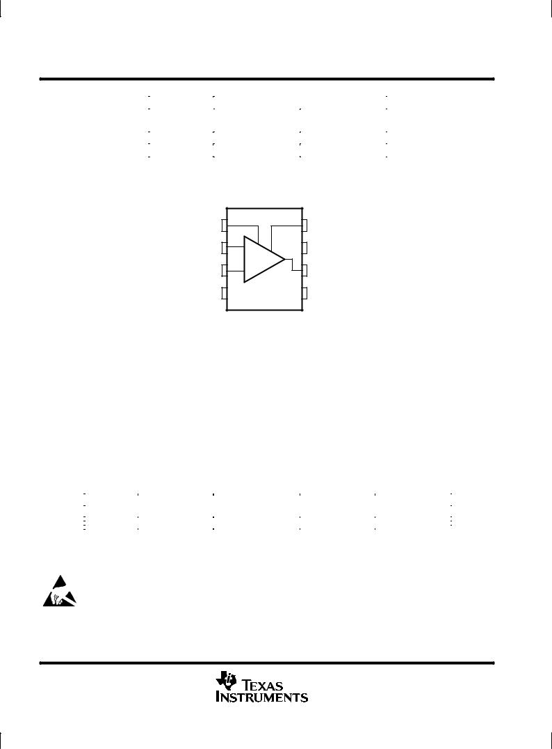
D |
Very High Speed |
|
|
|
|
|
|
|
|
|
|
D PACKAGE |
|
|
|
|||||||||
|
± 270 MHz Bandwidth (Gain = 1, ±3 dB) |
|
|
|
|
|
|
|
|
|
|
|
(TOP VIEW) |
|
|
|
||||||||
|
|
|
|
|
|
|
|
|
|
|
|
|
|
|
|
|
|
|
|
|
|
|
||
|
± 400 V/μsec Slew Rate |
|
|
|
|
|
|
|
NULL |
|
|
|
|
|
|
|
|
|
NULL |
|||||
|
|
|
|
|
|
|
|
|
1 |
|
|
|
|
8 |
|
|||||||||
|
± |
40-ns Settling Time (0.1%) |
|
|
|
|
|
|
|
|
|
|
|
|
|
|||||||||
|
|
|
|
|
|
|
|
IN ± |
|
2 |
|
|
|
|
7 |
|
VCC+ |
|||||||
D High Output Drive, IO = 100 mA |
|
|
|
|
|
|
|
|
|
|
|
|
|
|||||||||||
|
|
|
|
|
|
|
|
|
|
|
|
|
||||||||||||
|
|
|
|
|
|
|
IN + |
|
3 |
|
|
|
|
6 |
|
OUT |
||||||||
D |
Excellent Video Performance |
|
|
|
|
|
|
|
|
|
|
|
|
|
||||||||||
|
|
|
|
|
|
|
VCC ± |
|
4 |
|
|
|
|
5 |
|
NC |
||||||||
|
|
|
|
|
|
|
|
|
|
|
|
|
||||||||||||
|
± 60 MHz Bandwidth (0.1 dB, G = 1) |
|
|
|
|
|
|
|
|
|
|
|
|
|
||||||||||
|
|
|
|
|
|
|
|
|
|
|
|
|
|
|
||||||||||
|
|
|
|
|
|
|
|
|
|
|
|
|
|
|
|
|
|
|
|
|
|
|
||
|
± |
0.04% Differential Gain |
|
|
|
|
|
|
|
NC ± No internal connection |
||||||||||||||
|
± |
0.15° Differential Phase |
|
|
|
|
|
|
|
|
|
|
|
|
|
|
|
|
|
|
|
|
|
|
D |
Very Low Distortion |
|
|
|
|
|
|
|
|
|
|
|
|
|
|
|
|
|
|
|
|
|
|
|
|
± THD = ±72 dBc at f = 1 MHz |
|
|
|
|
|
|
|
|
|
CLOSED-LOOP GAIN |
|||||||||||||
|
|
|
|
|
|
|
|
|
|
|
|
|||||||||||||
D Wide Range of Power Supplies |
|
|
|
|
|
|
|
|
|
|
|
|
|
|
|
|
|
vs |
|
|
|
|||
|
VCC = ± 2.5 V to ± 15 V, |
|
|
|
|
|
|
|
|
|
|
|
|
FREQUENCY |
||||||||||
|
ICC = 7.5 mA |
8 |
|
|
|
|
|
|
|
|
|
|
|
|
|
|
|
|
|
|
|
|
|
|
|
|
|
|
|
|
|
|
|
|
|
|
|
|
|
|
|
|
|
|
|
|
|||
|
VCC = ±15 V |
|
|
|
|
|
||||||||||||||||||
D |
Evaluation Module Available |
6 |
|
|
|
|
|
|
||||||||||||||||
|
Gain = 1 |
|
|
|
|
|
|
|
|
|
|
|
|
|||||||||||
|
|
|
|
|
|
|
|
|
|
|
|
|
|
|
|
|
||||||||
description |
|
4 |
|
|
|
|
The THS4001 is a very high-performance, |
± dB |
2 |
|
|
|
|
0 |
|
|
|
|
||
voltage-feedback operational amplifier especially |
Gain |
|
|
|
|
|
suited for a wide range of video applications. The |
±2 |
|
|
|
|
|
-Loop |
|
|
|
|
||
device is specified to operate over a wide range of |
±4 |
|
3.9 pF |
|
|
|
supply voltages from ± 15 V to ± 2.5 V. With a |
|
|
|
|
||
bandwidth of 270 MHz, a slew rate of over |
Closed |
±6 |
|
200 Ω |
|
|
|
|
|
|
|||
400 V/μs, and settling times of less than 30 ns, the |
±8 |
|
± |
|
|
|
THS4001 offers the unique combination of high |
|
|
|
|
||
|
|
|
+ |
|
|
|
performance in an easy to use voltage feedback |
|
±10 |
|
|
|
|
|
|
50 Ω |
|
|
||
configuration over a wide range of power supply |
|
|
|
|
|
|
|
±12 |
|
|
|
|
|
voltages. |
|
|
|
|
|
|
|
|
|
|
|
|
|
The THS4001 is stable at all gains for both |
|
±14 |
1M |
10M |
100M |
1G 3G |
|
300k |
|||||
inverting and noninverting configurations. It has a |
|
|
|
f ± Frequency ± Hz |
|
|
high output drive capability of 100 mA and draws |
|
|
|
|
|
|
only 7.5 mA of quiescent current. Excellent professional video results can be obtained with the differential gain/phase performance of 0.04%/0.15° and 0.1 dB gain flatness to 60 MHz. For applications requiring low distortion, the THS4001 is ideally suited with total harmonic distortion of ±72 dBc at f = 1 MHz.
HIGH-SPEED AMPLIFIER FAMILY
|
ARCH. |
|
SUPPLY |
|
BW |
SR |
THD |
ts |
DIFF. |
DIFF. |
Vn |
|
||||
|
|
VOLTAGE |
|
|||||||||||||
DEVICE |
|
|
|
f = 1 MHz |
0.1% |
|
||||||||||
|
|
|
|
|
|
|
(MHz) |
(V/μs) |
GAIN |
PHASE |
|
|
|
|||
|
|
|
|
|
|
|
(nV/√ Hz |
) |
||||||||
|
VFB |
CFB |
5 V |
|
±5 V |
|
±15 V |
(dB) |
(ns) |
|||||||
|
|
|
|
|
|
|
|
|
|
|||||||
|
|
|
|
|
|
|
|
|
|
|
|
|
|
|
|
|
THS3001 |
|
• |
|
|
• |
|
• |
420 |
6500 |
±96 |
40 |
0.01% |
0.02° |
1.6 |
|
|
|
|
|
|
|
|
|
|
|
|
|
|
|
|
|
|
|
THS4001 |
• |
|
• |
|
• |
|
• |
270 |
400 |
±72 |
40 |
0.04% |
0.15° |
12.5 |
|
|
|
|
|
|
|
|
|
|
|
|
|
|
|
|
|
|
|
THS4031/32 |
• |
|
|
|
• |
|
• |
100 |
100 |
±72 |
60 |
0.02% |
0.03° |
1.6 |
|
|
|
|
|
|
|
|
|
|
|
|
|
|
|
|
|
|
|
THS4061/62 |
• |
|
|
|
• |
|
• |
180 |
400 |
±72 |
40 |
0.02% |
0.02° |
14.5 |
|
|
Please be aware that an important notice concerning availability, standard warranty, and use in critical applications of Texas Instruments semiconductor products and disclaimers thereto appears at the end of this data sheet.
PRODUCTION DATA information is current as of publication date. Products conform to specifications per the terms of Texas Instruments standard warranty. Production processing does not necessarily include testing of all parameters.
Copyright 1999, Texas Instruments Incorporated
POST OFFICE BOX 655303 •DALLAS, TEXAS 75265 |
1 |
THS4001
270-MHz HIGH-SPEED AMPLIFIER
SLOS206A± DECEMBER 1997 ± REVISED MARCH 1999
AVAILABLE OPTIONS
|
PACKAGED DEVICES |
|
TA |
|
|
SMALL OUTLINE² |
EVALUATION |
|
|
(D) |
MODULE |
|
|
|
0°C to 70°C |
THS4001CD |
THS4001EVM |
|
|
|
± 40°C to 85°C |
THS4001ID |
Ð |
|
|
|
²The D packages are available taped and reeled. Add an R suffix to the device type (i.e., THS4001CDR).
symbol
NULL
IN ±
IN +
VCC ±
|
NULL |
_ |
VCC + |
|
|
+ |
OUT |
|
NC |
absolute maximum ratings over operating free-air temperature (unless otherwise noted)²
Supply voltage, VCC± to VCC+ . . . . . . . . . . . . . . . . . . . . . . . . . . . . . . . . . . . . . . . . . . . . . . . . . . . . . . . . . . . . . . . 33 V Input voltage, VI . . . . . . . . . . . . . . . . . . . . . . . . . . . . . . . . . . . . . . . . . . . . . . . . . . . . . . . . . . . . . . . . . . . . . . . . . . . ± VCC Output current, IO . . . . . . . . . . . . . . . . . . . . . . . . . . . . . . . . . . . . . . . . . . . . . . . . . . . . . . . . . . . . . . . . . . . . . . . 175 mA Differential input voltage, VID . . . . . . . . . . . . . . . . . . . . . . . . . . . . . . . . . . . . . . . . . . . . . . . . . . . . . . . . . . . . . . . . . ± 4 V Continuous total power dissipation . . . . . . . . . . . . . . . . . . . . . . . . . . . . . . . . . . . . . See Dissipation Ratings Table
Operating free air temperature, TA: C suffix . . . . . . . . . . . . . . . . . . . . . . . . . . . . . . . . . . . . . . . . . . . . . 0°C to 70 °C I suffix . . . . . . . . . . . . . . . . . . . . . . . . . . . . . . . . . . . . . . . . . . . ±40°C to 85 °C
Storage temperature, Tstg . . . . . . . . . . . . . . . . . . . . . . . . . . . . . . . . . . . . . . . . . . . . . . . . . . . . . . . . ±65°C to 150 °C Lead temperature 1,6 mm (1/16 Inch) from case for 10 seconds . . . . . . . . . . . . . . . . . . . . . . . . . . . . . . . . 300°C
²Stresses beyond those listed under ªabsolute maximum ratingsº may cause permanent damage to the device. These are stress ratings only, and functional operation of the device at these or any other conditions beyond those indicated under ªrecommended operating conditionsº is not implied. Exposure to absolute-maximum-rated conditions for extended periods may affect device reliability.
DISSIPATION RATING TABLE
PACKAGE |
TA ≤ 25°C |
DERATING FACTOR |
TA = 70°C |
TA = 85°C |
|
POWER RATING |
ABOVE TA = 25°C |
POWER RATING |
POWER RATING |
||
|
|||||
D |
740 mW |
6 mW/°C |
475 mW |
385 mW |
CAUTION: The THS4001 provides ESD protection circuitry. However, permanent damage can still occur if this device is subjected to high-energy electrostatic discharges. Proper ESD precautions are recommended to avoid any performance degradation or loss of functionality
2 |
POST OFFICE BOX 655303 •DALLAS, TEXAS 75265 |
THS4001
270-MHz HIGH-SPEED AMPLIFIER
SLOS206A± DECEMBER 1997 ± REVISED MARCH 1999
recommended operating conditions
|
|
MIN |
TYP |
MAX |
UNIT |
|
|
|
|
|
|
Supply voltage, VCC |
Dual supply |
± 2.5 |
|
±16 |
V |
|
|
|
|
||
Single supply |
5 |
|
32 |
||
|
|
|
|||
|
|
|
|
|
|
Quiescent current, ICC |
± 15 V |
|
7.8 |
9.5 |
mA |
|
|
|
|
||
± 5 V, ± 2.5 V |
|
6.7 |
8 |
||
|
|
|
|||
|
|
|
|
|
|
Operating free-air temperature, TA |
C suffix |
0 |
|
70 |
°C |
|
|
|
|
||
I suffix |
± 40 |
|
85 |
||
|
|
|
electrical characteristics, VCC = ±15 V, RL = 150 Ω, TA = 25°C (unless otherwise noted)
|
PARAMETER |
TEST CONDITIONS |
VCC |
MIN |
TYP |
MAX |
UNIT |
|
|
|
Differential gain error |
|
|
±15 V |
|
0.04% |
|
|
|
|
|
|
|
|
|
|
|
|
|
|
Gain = 2, |
RL = 150 Ω, |
± 5 V |
|
0.01% |
|
|
|
|
|
|
|
|
|
|
||||
|
|
f = 3.58 MHz |
|
± |
|
° |
|
|
|
|
Differential phase error |
|
|
15 V |
|
0.15 |
|
|
|
|
|
|
± 5 V |
|
0.08° |
|
|
|
|
|
|
|
|
|
|
|
|
||
|
|
|
|
|
|
|
|
|
|
VIO |
Input offset voltage |
TA = 25°C |
|
±15 V, |
|
2 |
8 |
mV |
|
TA = full range |
|
± 5 V |
|
|
10 |
|
|||
|
|
|
|
|
|
|
|||
|
|
TA = 25°C |
|
±15 V, |
|
2.6 |
5 |
μ |
|
IIB |
Input bias current |
TA = full range |
|
± 5 V |
|
|
6 |
A |
|
|
|
|
|
|
|
|
|||
|
|
|
|
|
|
|
|
||
IOS |
Input offset current |
TA = 25°C |
|
±15 V, |
|
35 |
200 |
nA |
|
TA = full range |
|
± 5 V |
|
|
500 |
|
|||
|
|
|
|
|
|
|
|||
|
|
|
|
|
|
|
|
||
|
|
VO = ±10 V, |
TA = 25°C |
±15 V |
5 |
10 |
|
|
|
|
Open-loop gain |
RL = 1 kΩ |
TA = full range |
3 |
|
|
V/mV |
|
|
|
|
|
|
|
|||||
|
VO = ± 2.5 V, |
TA = 25°C |
± 5 V |
3 |
6 |
|
|
||
|
|
|
|
|
|||||
|
|
RL = 500 Ω |
TA = full range |
2 |
|
|
|
|
|
|
|
|
|
|
|
|
|||
CMRR |
Common-mode rejection ratio |
V(CM) = ± 12 V |
TA = 25°C |
±15 V |
85 |
100 |
|
dB |
|
TA = full range |
75 |
|
|
|
|||||
|
|
|
|
|
|
|
|
||
PSRR |
Power supply rejection ratio |
TA = 25°C |
|
±15 V, |
75 |
85 |
|
dB |
|
TA = full range |
|
± 5 V |
70 |
|
|
|
|||
|
|
|
|
|
|
|
|||
|
|
|
|
|
|
|
|
||
|
|
|
|
|
13.5 |
14.8 |
|
|
|
|
|
|
|
±15 V |
to |
to |
|
|
|
VICR |
Common-mode input voltage range |
|
|
|
±13 |
±14 |
|
V |
|
|
|
|
|
|
|
|
|||
|
|
|
3.6 |
4.4 |
|
|
|||
|
|
|
|
|
|
|
|
||
|
|
|
|
± 5 V |
to |
to |
|
|
|
|
|
|
|
|
± 2.7 |
± 3.6 |
|
|
|
|
|
|
|
|
|
|
|
|
|
|
|
|
|
±15 V |
± 13 |
± 13.5 |
|
|
|
|
|
RL = 500 Ω |
|
|
|
|
|
|
|
VO |
Output voltage swing |
|
± 5 V |
± 3.3 |
± 3.8 |
|
V |
|
|
|
|
|
|
± 2.5 V |
± 0.8 |
± 1.3 |
|
|
|
|
|
|
|
|
|
|
|
|
|
|
|
|
|
± 15 V |
50 |
100 |
|
|
|
|
|
|
|
|
|
|
|
|
|
IO |
Output current |
|
|
± 5 V |
50 |
100 |
|
mA |
|
|
|
|
|
± 2.5 V |
50 |
100 |
|
|
|
|
|
|
|
|
|
|
|
|
|
THD |
Total harmonic distortion |
VI = 1 V(PP), |
f = 1 MHz |
±15 V |
|
± 72 |
|
dBc |
|
RI |
Input resistance |
|
|
|
|
10 |
|
MΩ |
|
CI |
Input capacitance |
|
|
|
|
1.5 |
|
pF |
|
RO |
Output resistance |
Open loop |
|
|
|
10 |
|
Ω |
|
|
|
|
|
|
|
|
|
|
|
|
|
|
|
|
|
|
|
|
|
POST OFFICE BOX 655303 •DALLAS, TEXAS 75265 |
3 |

THS4001
270-MHz HIGH-SPEED AMPLIFIER
SLOS206A± DECEMBER 1997 ± REVISED MARCH 1999
operating characteristics, VCC = ±15 V, RL = 150 Ω, TA = 25°C (unless otherwise noted)
|
PARAMETER |
TEST CONDITIONS |
VCC |
MIN TYP |
MAX |
UNIT |
|||
|
|
|
|
±15 V |
400 |
|
|
|
|
|
|
|
|
|
|
|
V/μs |
||
|
Slew rate |
Gain = ±1 |
|
± 5 V |
400 |
|
|||
|
|
|
|
|
|
|
|
|
|
|
|
|
|
± 2.5 V |
350 |
|
|
|
|
|
|
|
|
|
|
|
|
|
|
|
Settling time to 0.1% |
10 V step (0 to 10 V), |
Gain = ±1 |
±15 V |
40 |
|
ns |
||
|
|
|
|
|
|
||||
|
± 2.5 V to 2.5 V step, |
Gain = ±1 |
± 5 V |
30 |
|
||||
|
|
|
|
|
|
||||
|
|
|
|
|
|
|
|
|
|
|
|
Gain = +1, |
RL = 150 Ω, |
±15 V |
270 |
|
|
|
|
|
|
|
|
|
|
|
|
||
|
|
± 5 V |
220 |
|
MHz |
||||
|
|
Rf = 150 Ω |
|
|
|
|
|
|
|
|
±3 dB Bandwidth |
|
± 2.5 V |
180 |
|
|
|
|
|
|
|
|
|
|
|
|
|||
|
|
|
|
|
|
|
|
|
|
|
Gain = ±1, |
RL = 150 Ω, |
±15 V |
80 |
|
|
|
|
|
|
|
|
|
|
|
||||
|
|
|
|
|
|
|
|
||
|
|
± 5 V |
75 |
|
MHz |
||||
|
|
Rf = 150 Ω |
|
|
|
|
|
|
|
|
|
|
± 2.5 V |
70 |
|
|
|
|
|
|
|
|
|
|
|
|
|
||
|
|
|
|
|
|
|
|
|
|
|
|
|
|
±15 V |
60 |
|
|
|
|
|
|
|
|
|
|
|
|
|
|
|
Bandwidth for 0.1 dB flatness |
Gain = +1 |
|
± 5 V |
50 |
|
MHz |
||
|
|
|
|
|
|
|
|
|
|
|
|
|
|
± 2.5 V |
40 |
|
|
|
|
|
|
|
|
|
|
|
|
|
|
|
|
|
|
±15 V, |
|
|
|
|
|
Vn |
Equivalent input noise voltage |
f = 10 kHz |
|
12.5 |
|
nV/√ Hz |
|||
|
± 5 V |
|
|||||||
|
|
|
|
±15 V, |
|
|
|
|
|
In |
Equivalent input noise current |
f = 10 kHz |
|
1.5 |
|
pA/√ Hz |
|||
|
± 5 V |
|
|||||||
TYPICAL CHARACTERISTICS
Table of Graphs
|
|
|
|
FIGURE |
|
|
|
|
|
|
|
|
IIB |
Input bias current |
vs Free-air temperature |
1 |
|
|
VIO |
Input offset voltage |
vs Free-air temperature |
2 |
|
|
|
Open-loop gain |
vs Frequency |
3 |
|
|
|
|
|
|
|
|
|
Phase |
vs Frequency |
3 |
|
|
|
|
|
|
|
|
|
Differential gain |
vs DC voltage |
4, 5 |
|
|
|
|
|
|
|
|
|
Differential phase |
vs DC voltage |
4, 5 |
|
|
|
|
|
|
|
|
|
Closed-loop gain |
vs Frequency |
6, 7 |
|
|
|
|
|
|
|
|
CMRR |
Common-mode rejection ratio |
vs Frequency |
8 |
|
|
|
|
|
|
|
|
PSRR |
Power-supply rejection ratio |
vs Frequency |
9 |
|
|
|
|
|
||
|
vs Free-air temperature |
10 |
|
||
|
|
|
|
||
|
|
|
|
|
|
|
VO(PP) |
Output voltage swing |
vs Supply voltage |
11 |
|
|
|
|
|
||
|
vs Load resistance |
12 |
|
||
|
|
|
|
||
|
|
|
|
|
|
|
|
Bandwidth (± 3 dB) |
vs Feedback resistance |
13, 14 |
|
|
|
|
|
|
|
|
ICC |
Supply current |
vs Supply voltage |
15 |
|
|
|
|
|
||
|
vs Free-air temperature |
16 |
|
||
|
|
|
|
||
|
|
|
|
|
|
|
Env |
Noise spectral density |
vs Frequency |
17 |
|
|
THD |
Total harmonic distortion |
vs Frequency |
18 |
|
|
|
|
|
|
|
|
|
|
|
|
|
4 |
POST OFFICE BOX 655303 •DALLAS, TEXAS 75265 |

|
THS4001 |
|
|
270-MHz HIGH-SPEED AMPLIFIER |
|
|
SLOS206A± DECEMBER 1997 ± REVISED MARCH 1999 |
|
|
|
|
TYPICAL CHARACTERISTICS |
||
INPUT BIAS CURRENT |
INPUT OFFSET VOLTAGE |
|
vs |
vs |
|
FREE-AIR TEMPERATURE |
FREE-AIR TEMPERATURE |
|
|
3 |
|
|
|
|
|
|
|
|
1.5 |
|
|
|
|
|
|
|
|
2.75 |
|
|
|
|
|
|
|
|
1 |
|
|
|
|
|
|
|
μ A |
|
|
|
|
|
|
|
|
mV |
|
|
|
|
|
|
|
|
± |
|
|
|
|
|
|
|
|
± |
|
|
|
|
|
|
|
|
Current |
2.5 |
|
|
|
|
|
|
|
Voltage |
0.5 |
|
|
|
|
VCC = ±15 V |
|
|
|
|
|
|
|
|
|
|
|
|
|
|
|
|
||||
|
|
|
|
|
|
VCC = ±15 V |
|
|
|
|
|
|
|
|
|||
BiasInput± |
|
|
|
|
|
|
OffsetInput |
|
|
|
|
|
|
|
|
||
2.25 |
|
|
|
|
|
|
|
0 |
|
|
|
|
|
|
|
||
|
|
|
|
|
|
|
|
|
|
|
|
|
|
|
|
||
|
2 |
|
|
|
|
VCC = ±5 V |
|
|
± 0.5 |
VCC = ±5 V |
|
|
|
|
|
||
|
|
|
|
|
|
|
|
|
|
|
|
|
|
|
|
||
IB |
|
|
|
|
|
VCC = ±2.5 V |
|
± |
|
|
|
|
|
|
|
|
|
I |
|
|
|
|
|
|
IO |
|
|
|
|
|
|
|
|
||
|
1.75 |
|
|
|
|
|
|
|
V |
±1 |
|
|
|
|
|
|
|
|
|
|
|
|
|
|
|
|
|
|
|
|
|
|
|
||
|
1.5 |
±20 |
0 |
20 |
40 |
60 |
80 |
100 |
|
± 1.5 |
±20 |
0 |
20 |
40 |
60 |
80 |
100 |
|
±40 |
|
±40 |
||||||||||||||
|
|
|
TA ± Free-Air Temperature ± °C |
|
|
|
|
|
TA ± Free-Air Temperature ± °C |
|
|
||||||
Figure 1 |
Figure 2 |
OPEN-LOOP GAIN AND PHASE
|
|
|
|
vs |
|
|
|
|
|
|
|
FREQUENCY |
|
|
|
||
|
90 |
|
|
|
|
|
|
|
|
80 |
|
|
|
VCC = ±15 V |
|
|
|
|
|
|
|
|
|
|
|
|
|
70 |
|
|
|
|
|
|
|
|
60 |
|
|
|
|
|
° |
|
± dB |
|
|
|
|
|
|
0 |
|
50 |
|
|
|
|
|
|
|
|
Loop Gain |
|
|
|
|
|
|
|
|
40 |
|
|
|
|
|
45° |
Phase |
|
30 |
|
|
|
|
|
|
||
|
|
|
|
|
|
|
||
- |
|
|
|
|
|
|
|
|
Open |
20 |
|
|
|
|
|
90° |
|
10 |
|
|
|
|
|
|
|
|
|
|
|
|
|
|
|
|
|
|
0 |
|
|
|
|
|
135 |
|
|
±10 |
|
|
|
|
|
° |
|
|
|
|
|
|
|
|
|
|
|
±20 |
|
|
|
|
|
180 |
|
|
1k |
10k |
100k |
1M |
10M |
100M |
1G5° |
|
|
|
|
f ± Frequency ± Hz |
|
|
|
||
Figure 3
POST OFFICE BOX 655303 •DALLAS, TEXAS 75265 |
5 |
 Loading...