


THS1408QPHP
|
THS1401 |
|
THS1403 |
www.ti.com |
THS1408 |
SLAS248D − DECEMBER 1999 − REVISED SEPTEMBER 2005
14 Bit, 1/3/8 MSPS, DSP COMPATIBLE ANALOG TO DIGITAL CONVERTERS WITH INTERNAL REFERENCE AND PGA
FEATURES |
DESCRIPTION |
D14-Bit Resolution
D1, 3, and 8 MSPS Speed Grades Available
DDifferential Nonlinearity (DNL) ±0.6 LSB Typ
DIntegral Nonlinearity (INL) ±1.5 LSB Typ
DInternal Reference
DDifferential Inputs
DProgrammable Gain Amplifier
DP-Compatible Parallel Interface
DTiming Compatible With TMS320C6000 DSP
D3.3-V Single Supply
DPower-Down Mode
DMonolithic CMOS Design
APPLICATIONS
DxDSL Front Ends
DCommunication
DIndustrial Control
DInstrumentation
DAutomotive
The THS1401, THS1403, and THS1408 are 14-bit, 1/3/8 MSPS, single supply analog-to-digital converters (ADCs) with an internal reference, differential inputs, programmable input gain, and an on-chip sample-and-hold amplifier.
Implemented with a CMOS process, the device has outstanding price/performance and power/speed ratios. The THS1401, THS1403, and THS1408 are designed for use with 3.3-V systems, and with a high-speed P- compatible parallel interface, making them the first choice for solutions based on high-performance DSPs such as the TI TMS320C6000 series.
The THS1401, THS1403, and THS1408 are available in a TQFP-48 package in standard commercial and industrial temperature ranges. The THS1401, THS1403, and THS1408 are also available in a PQFP-48 package in automotive temperature range, and the THS1408 is available in a PQFP-48 package in military temperature range.
VBG |
REF |
|
|
REF+ |
|
|
|
REF− |
|
1.5 V |
|
|
|
|
|
|
|
|
|
BG |
|
|
|
|
IN+ |
|
14 |
|
15 |
PGA |
14-Bit |
|
||
|
Buffer |
D[13:0] + OV bit |
||
0..7 dB |
ADC |
|
||
|
|
|||
|
|
|
||
IN− |
|
|
|
|
6 |
|
|
|
|
|
CONTROL |
|
|
A[1:0] |
CLK |
|
|
CS |
|
|
LOGIC |
|
|
WR |
|
|
|
|
OE |
Please be aware that an important notice concerning availability, standard warranty, and use in critical applications of Texas Instruments semiconductor products and disclaimers thereto appears at the end of this data sheet.
All trademarks are the property of their respective owners.
PRODUCTION DATA information is current as of publication date. Products conform to specifications per the terms of Texas Instruments standard warranty. Production processing does not necessarily include testing of all parameters.
Copyright 1999−2005, T exas Instruments Incorporated
On products compliant to MIL PRF 38535, all parameters are tested unless otherwise noted. On all other products, production processing does not necessarily include testing of all parameters.
www.ti.com

THS1401
THS1403
THS1408 |
www.ti.com |
SLAS248D − DECEMBER 1999 − REVISED SEPTEMBER 2005 |
|
ABSOLUTE MAXIMUM RATINGS |
|
Over operating free-air temperature range unless otherwise noted.(1) |
|
Supply voltage, (AVDD to AGND) . . . . . . . . . . . . . . . . . . . . . . . . . . . . . . . . . . . . . . . . . . . |
. . . . . . . . . . . . . . . . . . 4V |
Supply voltage, (DVDD to DGND) . . . . . . . . . . . . . . . . . . . . . . . . . . . . . . . . . . . . . . . . . . . |
. . . . . . . . . . . . . . . . . 4V |
Reference input voltage range, VBG . . . . . . . . . . . . . . . . . . . . . . . . . . . . . . . . . . . . . . . |
− 0.3 V to AV DD + 0.3 V |
Analog input voltage range . . . . . . . . . . . . . . . . . . . . . . . . . . . . . . . . . . . . . . . . . . . . . . . . . |
− 0.3 V to AV DD + 0.3 V |
Digital input voltage range . . . . . . . . . . . . . . . . . . . . . . . . . . . . . . . . . . . . . . . . . . . . . . . . |
− 0.3 V to DV DD + 0.3 V |
Operating free-air temperature range, TA: C-suffix . . . . . . . . . . . . . . . . . . . . . . . . . . . . . |
. . . . . . . . . 0°C to 70°C |
I-suffix . . . . . . . . . . . . . . . . . . . . . . . . . . . . . |
. . . . . . . −40 °C to 85°C |
Q-suffix . . . . . . . . . . . . . . . . . . . . . . . . . . . . |
. . . . . −40 °C to 125°C |
M-suffix . . . . . . . . . . . . . . . . . . . . . . . . . . . . |
. . . . . −55 °C to 125°C |
Storage temperature range, Tstg . . . . . . . . . . . . . . . . . . . . . . . . . . . . . . . . . . . . . . . . . . . . |
. . . . . −65 °C to 150°C |
Lead temperature 1,6 mm (1/16 inch) from case for 10 seconds . . . . . . . . . . . . . . . . . |
. . . . . . . . . . . . . . 260°C |
(1)Stresses beyond those listed under absolute maximum ratings may cause permanent damage to the device. These are stress ratings only, and functional operation of the device at these or any other conditions beyond those indicated under recommended operating conditions is not implied.
Exposure to absolute-maximum-rated conditions for extended periods may affect device reliability.
Terminal Functions
|
|
|
|
|
TERMINAL |
I/O |
DESCRIPTION |
|
NAME |
|
NO. |
||||||
|
||||||||
|
|
|
||||||
|
|
|
|
|
|
|
|
|
A[1:0] |
|
40, 41 |
I |
Address input |
||||
|
|
|
|
|
|
|
|
|
AGND |
|
7,8, 44, 45, 46 |
|
Analog ground |
||||
|
|
|
|
|
|
|
|
|
AVDD |
|
2, 43, 47 |
|
Analog power supply |
||||
CLK |
|
32 |
I |
Clock input |
||||
|
|
|
|
|
|
|
|
|
CML |
|
4 |
|
Reference midpoint. This pin requires a 0.1- F capacitor to AGND. |
||||
|
|
|
|
|
|
|
|
|
|
|
|
|
|
|
37 |
I |
Chip select input. Active low. |
|
CS |
|
|
|
|
|||
|
|
|
|
|
|
|
|
|
DGND |
|
9, 15, 25, 33, 34 |
|
Digital ground |
||||
|
|
|
|
|
|
|
|
|
DVDD |
|
14, 20, 26, 30, 31, 42 |
|
Digital power supply |
||||
D[13:0] |
|
11, 12, 13, 16, 17, 18, |
I/O |
Data inputs/outputs |
||||
|
|
|
|
|
|
19, 21, 22, 23, 24, 27, |
|
|
|
|
|
|
|
|
28, 29 |
|
|
|
|
|
|
|
|
|
|
|
|
NC |
|
38, 39 |
|
No connection; do not use. Reserved. |
|||
|
|
|
|
|
|
|
|
|
|
IN+ |
|
48 |
I |
Positive differential analog input |
|||
|
|
|
|
|
|
|
|
|
|
IN− |
|
1 |
I |
Negative differential analog input |
|||
|
|
|
|
|
|
|
|
|
|
|
|
|
|
|
35 |
I |
Output enable. Active low. |
|
OE |
|
|
|
||||
|
|
|
|
|
|
|
||
|
OV |
|
10 |
O |
Out-of-range output |
|||
|
|
|
|
|
|
|
||
REF+ |
|
5 |
O |
Positive reference output. This pin requires a 0.1- F capacitor to AGND. |
||||
|
|
|
|
|
|
|
||
REF− |
|
6 |
O |
Negative reference output. This pin requires a 0.1- F capacitor to AGND. |
||||
|
|
|
|
|
|
|
||
VBG |
|
3 |
I |
Reference input. This pin requires a 1- F capacitor to AGND. |
||||
|
|
|
|
|
|
|||
|
|
|
|
|
|
36 |
I |
Write signal. Active low. |
|
WR |
|
|
|||||
|
|
|
|
|
|
|
|
|
2

|
THS1401 |
|
THS1403 |
www.ti.com |
THS1408 |
|
|
|
|
|
|
|
|
|
|
|
|
|
|
|
|
|
|
|
|
|
|
|
|
|
|
|
|
SLAS248D − DECEMBER 1999 − REVISED SEPTEMBER 2005 |
||||||||||||
|
|
|
|
|
|
|
|
|
|
|
|
|
|
|
|
|
|
|
|
|
|
|
|
|
|
|
||||||||||||||
|
|
|
|
|
|
|
|
|
|
|
|
PFB AND PHP PACKAGE |
|
|
|
|
|
|
|
|
|
|
|
|
|
|||||||||||||||
|
|
|
|
|
|
|
|
|
|
|
|
|
|
|
|
(TOP VIEW) |
|
|
|
|
|
|
|
|
|
|
|
|
|
|
|
|
|
|||||||
|
|
|
|
|
|
|
|
|
|
DD |
|
|
|
|
|
|
DD |
DD |
|
|
|
|
|
|
|
|
|
|
|
|
|
|
|
|
|
|||||
|
|
|
|
|
|
|
IN+ |
|
AV |
AGND |
|
AGND AGND AV |
DV A0 |
A1 |
NC |
NC |
|
CS |
|
|
|
|
|
|
|
|||||||||||||||
|
|
|
|
|
|
|
|
|
|
|
|
|
|
|
|
|
||||||||||||||||||||||||
|
|
|
|
|
|
|
|
|
|
|
|
|
|
|
|
|
|
|
|
|
|
|
|
|
|
|
|
|
|
|
|
|
|
|
|
|
|
|
||
|
|
|
|
|
|
|
|
|
|
|
|
|
|
|
|
|
|
|
|
|
|
|
|
|
|
|
|
|
|
|
|
|
|
|
|
|
|
|
|
|
|
|
|
|
48 47 46 45 44 43 42 41 40 39 38 37 |
|
|
|
|
|
|
|
|
|
|
||||||||||||||||||||||||||
|
|
|
|
|
|
|
|
|
|
|
|
|
||||||||||||||||||||||||||||
|
|
|
|
|
|
|
|
|
|
|
|
|
|
|
|
|
|
|
|
|
|
|
|
|
|
|
|
|
|
|
|
|
|
|
|
|
|
|
|
|
|
IN− |
|
|
1 |
|
|
|
|
|
|
|
|
|
|
|
|
|
|
|
|
|
|
|
|
|
36 |
|
|
|
WR |
|
|
||||||||
|
|
|
|
|
|
|
|
|
|
|
|
|
|
|
|
|
|
|
|
|
|
|
|
|
35 |
|
|
|
|
|
|
|||||||||
|
AVDD |
|
|
2 |
|
|
|
|
|
|
|
|
|
|
|
|
|
|
|
|
|
|
|
|
|
|
|
|
OE |
|
|
|||||||||
|
|
|
|
|
|
|
|
|
|
|
|
|
|
|
|
|
|
|
|
|
|
|
34 |
|
|
|
DGND |
|||||||||||||
|
VBG |
|
|
3 |
|
|
|
|
|
|
|
|
|
|
|
|
|
|
|
|
|
|
|
|
|
|
|
|
||||||||||||
|
|
|
|
|
|
|
|
|
|
|
|
|
|
|
|
|
|
|
|
|
|
|
|
|
33 |
|
|
|
DGND |
|||||||||||
|
CML |
|
|
4 |
|
|
|
|
|
|
|
|
|
|
|
|
|
|
|
|
|
|
|
|
|
|
|
|
||||||||||||
|
|
|
|
|
|
|
|
|
|
|
|
|
|
|
|
|
|
|
|
|
|
|
|
|
32 |
|
|
|
CLK |
|||||||||||
|
REF+ |
|
|
5 |
|
|
|
|
|
|
|
|
|
|
|
|
|
|
|
|
|
|
|
|
|
|
|
|
||||||||||||
|
|
|
|
|
|
|
|
|
|
|
|
|
|
|
|
|
|
|
|
|
|
|
|
|
31 |
|
|
|
DVDD |
|||||||||||
|
REF− |
|
|
6 |
|
|
|
|
|
|
|
|
|
|
|
|
|
|
|
|
|
|
|
|
|
|
|
|
||||||||||||
|
|
|
|
|
|
|
|
|
|
|
|
|
|
|
|
|
|
|
|
|
|
|
|
|
30 |
|
|
|
DVDD |
|||||||||||
|
AGND |
|
|
7 |
|
|
|
|
|
|
|
|
|
|
|
|
|
|
|
|
|
|
|
|
|
|
|
|
||||||||||||
|
|
|
8 |
|
|
|
|
|
|
|
|
|
|
|
|
|
|
|
|
|
|
|
|
|
29 |
|
|
|
D0 |
|||||||||||
|
AGND |
|
|
|
|
|
|
|
|
|
|
|
|
|
|
|
|
|
|
|
|
|
|
|
|
|
|
|||||||||||||
|
|
|
9 |
|
|
|
|
|
|
|
|
|
|
|
|
|
|
|
|
|
|
|
|
|
28 |
|
|
|
D1 |
|||||||||||
|
DGND |
|
|
|
|
|
|
|
|
|
|
|
|
|
|
|
|
|
|
|
|
|
|
|
|
|
|
|||||||||||||
|
|
|
10 |
|
|
|
|
|
|
|
|
|
|
|
|
|
|
|
|
|
|
|
|
|
27 |
|
|
|
D2 |
|||||||||||
|
OV |
|
|
|
|
|
|
|
|
|
|
|
|
|
|
|
|
|
|
|
|
|
|
|
|
|
|
|||||||||||||
|
|
|
|
|
|
|
|
|
|
|
|
|
|
|
|
|
|
|
|
|
|
|
|
|
26 |
|
|
|
DVDD |
|||||||||||
|
D13 |
|
|
11 |
|
|
|
|
|
|
|
|
|
|
|
|
|
|
|
|
|
|
|
|
|
|
|
|
||||||||||||
|
|
|
|
|
|
|
|
|
|
|
|
|
|
|
|
|
|
|
|
|
|
|
|
|
25 |
|
|
|
DGND |
|||||||||||
|
D12 |
|
|
12 |
|
|
|
|
|
|
|
|
|
|
|
|
|
|
|
|
|
|
|
|
|
|
|
|
||||||||||||
|
|
|
|
13 14 15 16 17 18 19 20 21 22 23 24 |
|
|
|
|
|
|
|
|
|
|
||||||||||||||||||||||||||
|
|
|
|
|
|
|
|
|
|
|
|
|
||||||||||||||||||||||||||||
|
|
|
|
|
|
|
|
|
|
|
|
|
|
|
|
|
|
|
|
|
|
|
|
|
|
|
|
|
|
|
|
|
|
|
|
|
|
|
|
|
|
|
|
|
|
|
|
D11 |
|
|
DD |
DGND |
|
D10 D9 D8 |
|
|
DD |
|
|
|
|
|
|
|
|
|
|
|
|
|
|
|
|
|
|||||||
|
|
|
|
|
|
|
|
DV |
|
D7 DV |
D6 |
D5 |
D4 D3 |
|
|
|
|
|
|
|
||||||||||||||||||||
|
|
|
|
|
|
|
|
|
|
NC − No internal connection |
|
|
|
|
|
|
|
|
|
|
|
|
|
|
|
|||||||||||||||
|
|
|
|
|
|
|
|
|
|
|
|
|
|
|
|
|
|
|
|
|
|
|
|
|
|
|
|
|||||||||||||
|
|
|
|
|
|
|
|
|
|
|
|
|
AVAILABLE OPTIONS |
|
|
|
|
|
|
|
|
|
|
|
|
|
||||||||||||||
|
|
|
|
|
|
|
|
|
|
|
|
|
|
|
|
|
|
|
|
|
|
|
|
|
|
|
|
|
||||||||||||
|
|
|
|
|
|
|
|
|
|
|
|
|
|
|
|
|
|
|
|
PACKAGED DEVICE |
|
|
|
|
|
|
|
|||||||||||||
|
TA |
|
|
|
|
|
|
|
|
|
|
|
|
|
|
|
|
|
|
|
|
|
|
|
||||||||||||||||
|
|
|
|
|
|
|
|
|
|
|
|
|
TQFP |
|
|
|
|
|
|
|
|
PQFP (Power Pad) |
|
|||||||||||||||||
|
|
|
|
|
|
|
|
|
|
|
|
|
|
|
|
(PFB) |
|
|
|
|
|
|
|
|
|
|
|
(PHP) |
|
|||||||||||
|
|
|
|
|
|
|
|
|
|
|
|
|
|
|
|
|
|
|
|
|
|
|
|
|
|
|
|
|
|
|
||||||||||
|
|
|
|
|
|
|
|
|
|
|
|
|
THS1401CPFB, |
|
|
|
|
|
|
|
|
|
|
|
|
|
|
|
|
|
||||||||||
|
0°C to 70°C |
|
|
|
|
|
THS1403CPFB, |
|
|
|
|
|
|
|
|
|
|
— |
|
|||||||||||||||||||||
|
|
|
|
|
|
|
|
|
|
|
|
|
THS1408CPFB |
|
|
|
|
|
|
|
|
|
|
|
|
|
|
|
|
|
||||||||||
|
|
|
|
|
|
|
|
|
|
|
|
|
|
|
|
|
|
|
|
|
|
|
|
|
|
|
|
|
|
|
||||||||||
|
|
|
|
|
|
|
|
|
|
|
|
|
THS1401IPFB, |
|
|
|
|
|
|
|
|
|
|
|
|
|
|
|
|
|
||||||||||
|
−40 °C to 85°C |
|
|
|
|
|
THS1403IPFB, |
|
|
|
|
|
|
|
|
|
|
— |
|
|||||||||||||||||||||
|
|
|
|
|
|
|
|
|
|
|
|
|
THS1408IPFB |
|
|
|
|
|
|
|
|
|
|
|
|
|
|
|
|
|
||||||||||
|
|
|
|
|
|
|
|
|
|
|
|
|
|
|
|
|
|
|
|
|
|
|
|
|
|
|
|
|
|
|||||||||||
|
|
|
|
|
|
|
|
|
|
|
|
|
|
|
|
|
|
|
|
|
|
|
|
|
|
|
|
THS1401QPHP, |
|
|||||||||||
|
−40 °C to 125°C |
|
|
|
|
|
|
|
|
|
— |
|
|
|
|
|
|
|
|
THS1403QPHP, |
|
|||||||||||||||||||
|
|
|
|
|
|
|
|
|
|
|
|
|
|
|
|
|
|
|
|
|
|
|
|
|
|
|
|
THS1408QPHP |
|
|||||||||||
|
|
|
|
|
|
|
|
|
|
|
|
|
|
|
|
|
|
|
|
|
|
|||||||||||||||||||
|
−55 °C to 125°C |
|
|
|
|
|
|
|
|
|
— |
|
|
|
|
|
|
|
|
THS1408MPHP |
|
|||||||||||||||||||
|
|
|
|
|
|
|
|
|
|
|
|
|
|
|
|
|
|
|
|
|
|
|
|
|
|
|
|
|
|
|
|
|
|
|
|
|
|
|
|
|
3

THS1401
THS1403
THS1408 |
|
www.ti.com |
||
SLAS248D − DECEMBER 1999 − REVISED SEPTEMBER 2005 |
|
|
|
|
THERMAL CHARACTERISTICS(1) |
|
|
||
|
|
TYP |
UNIT |
|
|
|
|
|
|
Thermal resistance, junction-to-ambient, ΘJA |
PFB package |
85.9 |
°C/W |
|
|
|
|||
PHP package |
28.8 |
|||
|
|
|||
|
|
|
|
|
Thermal resistance, junction-to-case, ΘJC |
PFB package |
19.6 |
°C/W |
|
|
|
|||
PHP package |
0.79 |
|||
|
|
|||
|
|
|
|
|
(1) Thermal resistance is modeled data, is not production tested, and is given for informational purposes only.
RECOMMENDED OPERATING CONDITIONS
|
|
MIN |
NOM |
MAX |
UNIT |
|
|
|
|
|
|
|
|
Supply voltage, AVDD, DVDD |
|
3 |
3.3 |
3.6 |
V |
|
High level digital input, VIH |
|
2 |
3.3 |
|
V |
|
Low level digital input, VIL |
|
|
0 |
0.8 |
V |
|
Load capacitance, CL |
|
|
5 |
15 |
pF |
|
|
THS1401 |
0.1 |
1 |
1 |
MHz |
|
|
|
|
|
|
|
|
Clock frequency, fCLK |
THS1403 |
0.1 |
3 |
3 |
MHz |
|
|
THS1408 |
0.1 |
8 |
8 |
MHz |
|
|
|
|
|
|
|
|
Clock duty cycle |
C- and I-suffix |
40 |
50 |
60 |
% |
|
|
|
|
|
|||
Q- and M-suffix |
45 |
50 |
55 |
|||
|
|
|||||
|
|
|
|
|
|
|
|
C-suffix |
0 |
25 |
70 |
|
|
|
|
|
|
|
|
|
Operating free-air temperature |
I-suffix |
−40 |
25 |
85 |
°C |
|
|
|
|
|
|||
Q-suffix |
−40 |
25 |
125 |
|||
|
|
|||||
|
|
|
|
|
|
|
|
M-suffix |
−55 |
25 |
125 |
|
|
|
|
|
|
|
|
4

THS1401
THS1403
www.ti.com |
|
|
|
|
THS1408 |
||
|
|
|
SLAS248D − DECEMBER 1999 − REVISED SEPTEMBER 2005 |
||||
ELECTRICAL CHARACTERISTICS |
|
|
|
|
|
||
Over operating free-air temperature range, AVDD = DVDD = 3.3V, unless otherwise noted. |
|
|
|
|
|||
|
|
|
|
|
|
|
|
|
PARAMETER |
TEST CONDITIONS |
MIN |
TYP |
MAX |
UNIT |
|
|
|
|
|
|
|
|
|
Power Supply |
|
|
|
|
|
|
|
|
|
|
|
|
|
|
|
IDDA |
Analog supply current |
|
AVDD = 3.6 V |
|
81 |
90 |
mA |
IDDD |
Digital supply current |
|
DVDD = 3.6 V |
|
5 |
10 |
mA |
|
Power |
|
AVDD = DVDD = 3.6 V |
|
270 |
360 |
mW |
|
Power down current |
|
|
|
20 |
|
A |
|
|
|
|
|
|
|
|
DC Characteristics |
|
|
|
|
|
|
|
|
|
|
|
|
|
|
|
|
Resolution |
|
|
|
14 |
|
Bits |
|
|
|
|
|
|
|
|
DNL |
Differential nonlinearity |
|
|
|
±0.6 |
±1 |
LSB |
|
|
|
|
|
|
|
|
|
|
THS1401 |
|
|
±1.5 |
±2.5 |
|
|
|
|
|
|
|
|
|
|
|
THS1403C/I |
|
|
±1.5 |
±2.5 |
|
|
|
|
|
|
|
|
|
INL |
Integral nonlinearity |
THS1403Q |
Best fit |
|
±2 |
±3 |
LSB |
|
|
THS1408C/I |
|
|
±3 |
±5 |
|
|
|
|
|
|
|
|
|
|
|
THS1408Q/M |
|
|
±3.5 |
±7.5 |
|
|
|
|
|
|
|
|
|
|
Offset error |
|
IN+ = IN−, PGA = 0 dB |
|
|
0.3 |
%FSR |
|
|
|
|
|
|
|
|
|
Gain error |
C and I suffix |
PGA = 0 dB |
|
|
1 |
%FSR |
|
|
|
|
|
|
||
|
Q and M suffix |
|
|
1.75 |
%FSR |
||
|
|
|
|
|
|||
|
|
|
|
|
|
|
|
AC Characteristics |
|
|
|
|
|
|
|
|
|
|
|
|
|
|
|
ENOB |
Effective number of bits |
|
|
11.2 |
11.5 |
|
Bits |
|
|
|
|
|
|
|
|
|
|
THS1401/3/8 |
fi = 100 kHz |
|
−81 |
|
|
THD |
Total harmonic distortion |
THS1403/8 |
fi = 1 MHz |
|
−78 |
|
dB |
|
|
THS1408 |
fi = 4 MHz |
|
−77 |
|
|
|
|
THS1401/3/8 |
fi = 100 kHz |
|
72 |
|
|
SNR |
Signal-to-noise ratio |
THS1403/8 |
fi = 1 MHz |
70 |
72 |
|
dB |
|
|
THS1408 |
fi = 4 MHz |
|
71 |
|
|
|
|
THS1401/3/8 |
fi = 100 kHz |
|
70 |
|
|
SINAD |
Signal-to-noise ratio + distortion |
THS1403/8 |
fi = 1 MHz |
69 |
70 |
|
dB |
|
|
THS1408 |
fi = 4 MHz |
|
70 |
|
|
|
|
THS1401/3/8 |
fi = 100 kHz |
|
80 |
|
|
SFDR |
Spurious-free dynamic range |
THS1403C/I, THS1408C/I |
fi = 1 MHz |
73 |
80 |
|
dB |
|
|
|
|
||||
THS1403Q, THS1408Q/M |
71 |
80 |
|
||||
|
|
|
|
|
|||
|
|
|
|
|
|
|
|
|
|
THS1408 |
fi = 4 MHz |
|
80 |
|
|
|
Analog input bandwidth |
|
|
|
140 |
|
MHz |
|
|
|
|
|
|
|
|
5

THS1401
THS1403
THS1408 |
www.ti.com |
SLAS248D − DECEMBER 1999 − REVISED SEPTEMBER 2005 |
|
ELECTRICAL CHARACTERISTICS (Cont.)
Over operating free-air temperature range, AVDD = DVDD = 3.3V, unless otherwise noted.
|
PARAMETER |
TEST CONDITIONS |
MIN |
TYP |
MAX |
UNIT |
|
|
|
|
|
|
|
Reference Voltage |
|
|
|
|
|
|
|
|
|
|
|
|
|
|
Bandgap voltage, internal mode |
|
1.425 |
1.5 |
1.575 |
V |
|
|
|
|
|
|
|
|
Input impedance |
|
|
40 |
|
kΩ |
|
|
|
|
|
|
|
|
Positive reference voltage, REF+ |
|
|
2.5 |
|
V |
|
|
|
|
|
|
|
|
Negative reference voltage, REF− |
|
|
0.5 |
|
V |
|
|
|
|
|
|
|
|
Reference difference, ∆REF, REF+ − REF− |
|
|
2 |
|
V |
|
Accuracy, internal reference |
|
|
5% |
|
|
|
|
|
|
|
|
|
|
Temperature coefficient |
|
|
40 |
|
ppm/°C |
|
|
|
|
|
|
|
|
Voltage coefficient |
|
|
200 |
|
ppm/V |
|
|
|
|
|
|
|
Analog Inputs |
|
|
|
|
|
|
|
|
|
|
|
|
|
|
Positive analog input, IN+ |
|
0 |
|
AVDD |
V |
|
Negative analog input, IN− |
|
0 |
|
AVDD |
V |
|
Analog input voltage difference |
∆AIN = IN+ − IN−, V REF = REF+ − REF− |
−V REF |
|
VREF |
V |
|
Input impedance |
|
|
25 |
|
kΩ |
|
|
|
|
|
|
|
|
PGA range |
|
0 |
|
7 |
dB |
|
|
|
|
|
|
|
|
PGA step size |
|
|
1 |
|
dB |
|
|
|
|
|
|
|
|
PGA gain error |
|
|
|
±0.25 |
dB |
|
|
|
|
|
|
|
Digital Inputs |
|
|
|
|
|
|
|
|
|
|
|
|
|
VIH |
High-level digital input |
|
2 |
|
|
V |
VIL |
Low-level digital input |
|
|
|
0.8 |
V |
|
Input capacitance |
|
|
5 |
|
pF |
|
|
|
|
|
|
|
|
Input current |
|
|
|
±1 |
µA |
Digital Outputs |
|
|
|
|
|
|
|
|
|
|
|
|
|
VOH |
High-level digital output |
IOH = 50 µA |
2.6 |
|
|
V |
VOL |
Low-level digital output |
IOL = 50 µA |
|
|
0.4 |
V |
IOZ |
Output current, high impedance |
|
|
|
±10 |
µA |
Clock Timing (CS low) |
|
|
|
|
|
|
|
|
|
|
|
|
|
|
|
THS1401 |
0.1† |
1 |
1 |
MHz |
f |
Clock frequency |
THS1403 |
0.1† |
3 |
3 |
MHz |
CLK |
|
|
|
|
|
|
|
|
THS1408 |
0.1† |
8 |
8 |
MHz |
td |
Output delay time |
|
|
|
25 |
ns |
|
Latency |
|
|
9.5 |
|
Cycles |
|
|
|
|
|
|
|
†This parameter is not production tested for Q- and M-suffix devices.
6

|
THS1401 |
|
THS1403 |
www.ti.com |
THS1408 |
SLAS248D − DECEMBER 1999 − REVISED SEPTEMBER 2005
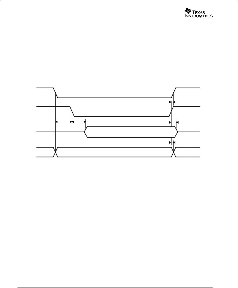
PARAMETER MEASUREMENT INFORMATION
sample timing
The THS1401/3/8 core is based on a pipeline architecture with a latency of 9.5 samples. The conversion results appear on the digital output 9.5 clock cycles after the input signal was sampled.
S11 |
S12 |
|
S9
Analog  S10
S10
Input
tw(CLK) |
tw(CLK) |
|
|
CLK |
|
|
|
|
td |
|
|
Data |
C1 |
C2 |
C3 |
|
Out
Figure 1. Sample Timing
The parallel interface of the THS1401/3/8 ADC features 3-state buffers, making it possible to directly connect it to a data bus. The output buffers are enabled by driving the OE input low.
Besides the sample results, it is also possible to read back the values of the control register, the PGA register, and the offset register. Which register is read is determined by the address inputs A[1,0]. The ADC results are available at address 0.
The timing of the control signals is described in the following sections.
7
THS1401
THS1403
THS1408 |
|
|
|
|
|
|
|
|
|
|
|
|
|
|
|
|
|
|
|
|
|
|
|
|
|
|
|
|
|
|
|
www.ti.com |
|||
SLAS248D − DECEMBER 1999 − REVISED SEPTEMBER 2005 |
|
|
|
|
|
|
|
|
|
|
|
|
|
|
|
|
|
||||||||||||||||||
|
|
|
|
|
|
|
|
PARAMETER MEASUREMENT INFORMATION |
|
|
|
||||||||||||||||||||||||
read timing (15-pF load) |
|
|
|
|
|
|
|
|
|
|
|
|
|
|
|
|
|
|
|||||||||||||||||
|
|
|
|
|
|
|
|
|
|
|
|
|
|
|
|
|
|
|
|
|
|
|
|
|
|
|
|
|
|
|
|
|
|
|
|
|
|
|
|
|
|
|
|
|
|
|
|
PARAMETER |
|
|
MIN |
TYP MAX |
UNIT |
||||||||||||||||||
|
|
|
|
|
|
|
|
|
|
|
|
|
|
|
|
|
|
|
|
|
|
|
|
|
|
|
|
|
|
|
|
|
|
|
|
tsu(OE−ACS) |
Address and chip select setup time |
|
|
4 |
|
|
|
|
|
|
ns |
||||||||||||||||||||||||
ten |
Output enable |
|
|
|
|
|
|
|
|
|
|
|
|
|
|
|
15 |
ns |
|||||||||||||||||
tdis |
Output disable |
|
|
|
|
|
|
|
|
|
|
|
|
|
|
|
10 |
ns |
|||||||||||||||||
th(A) |
Address hold time |
|
|
1 |
|
|
|
|
|
|
ns |
||||||||||||||||||||||||
th(CS) |
Chip select hold time |
|
|
0 |
|
|
|
|
|
|
ns |
||||||||||||||||||||||||
NOTE: All timing parameters refer to a 50% level. |
|
|
|
|
|
|
|
|
|
|
|
|
|
|
|
|
|
|
|||||||||||||||||
|
|
|
|
|
|
|
|
|
|
|
|
|
|
|
|
|
|
|
|
|
|
|
|
|
|
|
|
|
|
|
|
|
|
|
|
|
CS |
|
|
|
|
|
|
|
|
|
|
|
|
|
|
|
|
|
|
|
|
|
|
|
|
|
|
|
|
|
|
|
th(CS) |
|
|
|
|
|
|
|
|
|
|
|
|
|
|
|
|
|
|
|
|
|
|
|
|
|
|
|
|
|
|
|
|
|
|
|
|
||
|
|
|
|
|
|
|
|
|
|
|
|
|
|
|
|
|
|
|
|
|
|
|
|
|
|
|
|
|
|
|
|
|
|
||
|
|
|
|
|
|
|
|
|
|
|
|
|
|
|
|
|
|
|
|
|
|
|
|
|
|
|
|
|
|
|
|
|
|
|
|
|
OE |
|
|
|
|
|
|
|
|
|
|
|
|
|
|
|
|
|
|
|
|
|
|
|
|
|
|
|
|
|
|
|
|
|
|
|
tsu(OE−ACS) |
|
|
|
|
|
|
|
|
|
|
|
|
|
|
ten |
|
|
|
|
|
|
|
|
|
|
|
|
|
|
|
t |
|
||
|
|
|
|
|
|
|
|
|
|
|
|
|
|
|
|
|
|
|
|
|
|
|
|
|
|
|
|
||||||||
|
|
|
|
|
|
|
|
|
|
|
|
|
|
|
|
|
|
|
|
|
|
|
|
|
|
|
|
|
|
|
|||||
|
|
|
|
|
|
|
|
|
|
|
|
|
|
|
|
|
|
|
|
|
|
|
|
|
|
|
|
|
|
|
|
|
|
dis |
|
|
|
|
|
|
|
|
|
|
|
|
|
|
|
|
|
|
|
|
|
|
|
|
|
|
|
|
|
|
|
|
|||||
D[13:0] |
|
|
|
|
|
|
|
|
|
|
|
|
|
|
|
|
DATA |
|
|
|
|
|
|||||||||||||
O V |
|
|
|
|
|
|
|
|
|
|
|
|
|
|
|
|
|
|
|
|
|
|
|
|
|
|
|
|
|
|
|
|
|
||
A[1:0] |
|
|
|
|
|
|
|
|
|
|
|
|
|
|
|
|
|
|
|
|
|
|
|
|
|
|
|
|
|
|
th(A) |
|
|||
|
|
|
|
|
|
|
|
|
|
|
|
|
|
|
|
|
|
|
|
|
|
|
|
|
|
|
|
|
|
|
|||||
X |
|
|
|
|
|
|
|
|
|
|
|
|
|
ADDRESS |
|
|
|
|
|
|
|
X |
|
||||||||||||
|
|
|
|
|
|
|
|
|
|
|
|
|
|
|
|
|
|
||||||||||||||||||
Figure 2. Read Timing
8
 Loading...