


a10-Bit High Speed Multiplying D/A Converter
(Universal Digital Logic Interface)
DAC10*
FEATURES
Fast Settling: 85 ns
Low Full-Scale Drift: 10 ppm/8C
Nonlinearity to 0.05% Max Over Temperature Range Complementary Current Outputs: 0 mA to 4 mAÊ Wide Range Multiplying Capability: 1 MHz Bandwidth Wide Power Supply Range: +5, –7.5 Min to 618 V Max
Direct Interface to TTL, CMOS, ECL, PMOS, NMOS Availability in Die FormÊ
GENERAL DESCRIPTION
The DAC10 series of 10-bit monolithic multiplying digital-to- analog converters provide high speed performance and full-scale accuracy.
Advanced circuit design achieves 85 ns settling times with very low “glitch” energy and low power consumption. Direct interface to all popular logic families with full noise immunity is provided by the high swing, adjustable threshold logic inputs.
All DAC10 series models guarantee full 10-bit monotonicity, and nonlinearities as tight as +0.05% over the entire operating temperature range are available. Device performance is essentially unchanged over the ± 18 V power supply range, with 85 mW power consumption attainable at lower supplies.
A highly stable, unique trim method is used, which selectively shorts Zener diodes, to provide 1/2 LSB full-scale accuracy without the need for laser trimming.
Single-chip reliability, coupled with low cost and outstanding flexibility, make the DAC10 device an ideal building block for A/D converters, Data Acquisition systems, CRT displays, programmable test equipment and other applications where low power consumption, input/output versatility and long-term stability are required.
|
|
|
|
SIMPLIFIED SCHEMATIC |
|
|
|
|
|
||||
|
|
|
MSB |
|
|
|
|
|
|
|
|
LSB |
|
|
V+ |
VLC |
B1 |
B2 |
B3 |
B4 |
B5 |
B6 |
B7 |
B8 |
B9 |
B10 |
|
|
15 |
1 |
5 |
6 |
7 |
8 |
9 |
10 |
11 |
12 |
13 |
14 |
|
|
|
BIAS NETWORK |
|
|
|
|
|
|
|
|
|
4 |
IOUT |
|
|
|
|
|
|
|
|
|
|
|
|
|
|
16 |
CURRENT SWITCHES |
|
|
|
|
|
|
|
|
2 |
IOUT |
||
VREF (+) |
REFERENCE |
|
|
|
|
|
|
|
|
|
|
|
|
|
AMPLIFIER |
|
|
|
|
|
|
|
|
|
|
|
|
17 |
|
|
|
|
|
|
|
|
|
|
|
|
|
VREF (–) |
|
|
|
|
|
|
|
|
|
|
|
|
|
|
18 |
|
3 |
|
|
|
|
|
|
|
|
|
|
|
COMP |
|
V– |
|
|
|
|
|
|
|
|
|
|
*Protected by Patent Nos. 4,055,770, 4,056,740 and 4,092,639.
REV. D
Information furnished by Analog Devices is believed to be accurate and reliable. However, no responsibility is assumed by Analog Devices for its use, nor for any infringements of patents or other rights of third parties which may result from its use. No license is granted by implication or otherwise under any patent or patent rights of Analog Devices.
One Technology Way, P.O. Box 9106, Norwood, MA 02062-9106, U.S.A.
Tel: 781/329-4700 |
World Wide Web Site: http://www.analog.com |
Fax: 781/326-8703 |
© Analog Devices, Inc., 1998 |

DAC10–SPECIFICATIONS
|
|
|
|
|
|
|
(@ VS = 615 V; IREF = 2 mA; 08C ≤ TA ≤ +708C for DAC10F and G, unless otherwise noted. |
|||||||||
ELECTRICAL CHARACTERISTICS Output characteristics apply to both IOUT and |
|
.) |
|
|
|
|
||||||||||
IOUT |
|
|
|
|
||||||||||||
|
|
|
|
|
|
|
|
DAC10F |
|
|
|
DAC10G |
|
|
||
Parameter |
Symbol |
|
Conditions |
Min |
Typ |
Max |
Min |
Typ |
Max |
Units |
||||||
|
|
|
|
|
|
|
|
|
|
|
|
|
|
|
|
|
MONOTONICITY |
|
|
|
|
|
|
|
10 |
|
|
|
|
10 |
|
|
Bits |
|
|
|
|
|
|
|
|
|
|
|
|
|
|
|
|
|
NONLINEARITY |
NL |
|
|
|
|
|
|
|
0.3 |
0.5 |
|
|
0.6 |
1 |
LSB |
|
|
|
|
|
|
|
|
|
|
|
|
|
|
|
|
|
|
DIFFERENTIAL |
|
|
|
|
|
|
|
|
|
|
|
|
|
|
|
|
NONLINEARITY |
DNL |
|
|
|
|
|
|
|
0.3 |
1 |
|
|
|
0.7 |
|
LSB |
|
|
|
|
|
|
|
|
|
|
|
|
|
|
|
|
|
SETTLING TIME |
tS |
|
All Bits Switched ON or OFF |
|
|
|
|
|
|
|
|
|
||||
|
|
|
Settle to 0.05% of FS (See Note) |
|
85 |
135 |
|
|
85 |
150 |
ns |
|||||
|
|
|
|
|
|
|
|
|
|
|
|
|
|
|
|
|
OUTPUT CAPACITANCE |
CO |
|
|
|
|
|
|
|
18 |
|
|
|
|
18 |
|
pF |
PROPAGATION DELAY |
tPLH |
|
All Bits Switched RL = 5 kΩ |
|
50 |
|
|
|
|
50 |
|
ns |
||||
|
tPHL |
|
|
|
|
|
RL = 0 kΩ |
|
50 |
|
|
|
|
50 |
|
ns |
OUTPUT VOLTAGE |
|
|
Full-Scale Current Change |
|
–5.5 |
|
|
|
|
–5.5 |
|
V |
||||
COMPLIANCE |
VOC |
|
<1 LSB |
|
+10 |
|
|
|
|
+10 |
|
V |
||||
GAIN TEMPCO |
TCIFS |
|
(See Note) |
|
±10 |
±25 |
|
|
±10 |
±50 |
ppm/°C |
|||||
FULL-SCALE SYMMETRY |
IFSS |
|
|
|
|
|
|
|
|
|
|
|
|
|
|
μA |
|
IFR–IFR |
|
|
0.1 |
4 |
|
|
|
0.1 |
4 |
||||||
ZERO-SCALE CURRENT |
IZS |
|
|
|
|
|
|
|
0.01 |
0.5 |
|
|
0.01 |
0.5 |
μA |
|
FULL-SCALE CURRENT |
IFR |
|
(See Note) |
3.960 |
3.996 |
4.032 |
|
3.920 |
3.996 |
4.072 |
mA |
|||||
REFERENCE INPUT |
|
|
|
|
|
|
|
|
|
|
|
|
|
|
|
mA/μs |
SLEW RATE |
DI/dt |
|
|
|
|
|
|
|
6 |
|
|
|
|
6 |
|
|
|
|
|
|
|
|
|
|
|
|
|
|
|
|
|
|
|
REFERENCE BIAS |
|
|
|
|
|
|
|
|
|
|
|
|
|
|
|
μA |
CURRENT |
IB |
|
|
|
|
|
|
|
–1 |
–3 |
|
–1 |
–3 |
|||
POWER SUPPLY |
PPS/FS+ |
|
4.5 V ≤ V+ ≤ –18 V |
|
0.001 |
0.01 |
|
|
0.001 |
0.01 |
% IFS/% V |
|||||
SENSITIVITY |
PPS/FS– |
|
–18 V ≤ V– ≤ –10 V |
|
0.0012 |
0.01 |
|
|
0.0012 |
0.01 |
% IFS/% V |
|||||
POWER SUPPLY CURRENT |
I+ |
|
VS = ±15 V; IREF = 2 mA |
|
2.3 |
4 |
|
|
|
2.3 |
4 |
mA |
||||
|
I– |
|
|
|
|
|
|
|
–9 |
–15 |
|
–9 |
–15 |
mA |
||
|
I+ |
|
VS = +5 V; –7.5 V; IREF = 1 mA |
|
1.8 |
4 |
|
|
|
1.8 |
4 |
mA |
||||
|
I– |
|
|
|
|
|
|
|
–5.9 |
–9 |
|
–5.9 |
–9 |
mA |
||
|
|
|
|
|
|
|
|
|
|
|
|
|
|
|
|
|
POWER DISSIPATION |
PD |
|
VS = ±15 V; IREF = 2 mA |
|
231 |
285 |
|
|
231 |
285 |
mW |
|||||
|
PD |
|
VS = +5 V; –7.5 V; IREF = 1 mA |
|
85 |
88 |
|
|
|
85 |
88 |
mW |
||||
LOGIC INPUT LEVELS |
VIL |
|
VLC = 0 |
|
|
0.8 |
|
|
|
0.8 |
V |
|||||
|
VIH |
|
VLC = 0 |
2 |
|
|
|
|
2 |
|
|
V |
||||
LOGIC INPUT CURRENTS |
IIL |
|
VLC = 0; VIN = 0.8 V |
–10 |
–5 |
|
|
|
–10 |
–5 |
|
μA |
||||
|
IIH |
|
VIN = 2.0 V |
|
0.001 |
10 |
|
|
|
0.001 |
10 |
μA |
||||
|
|
|
|
|
|
|
(@ VS = 615 V; IREF = 2 mA; TA = +258C, unless otherwise noted. Output characteristics |
|||||||||
ELECTRICAL CHARACTERISTICS apply to both IOUT and IOUT |
.) |
|
|
|
|
|
|
|
|
|||||||
|
|
|
|
|
|
|
|
DAC10F |
|
|
|
DAC10G |
|
|
||
Parameter |
Symbol |
|
Conditions |
Min |
Typ |
Max |
Min |
Typ |
Max |
Units |
||||||
|
|
|
|
|
|
|
|
|
|
|
|
|
|
|
|
|
MONOTONICITY |
|
|
|
|
|
|
|
10 |
|
|
|
|
10 |
|
|
Bits |
|
|
|
|
|
|
|
|
|
|
|
|
|
|
|
|
|
NONLINEARITY |
NL |
|
|
|
|
|
|
|
0.3 |
0.5 |
|
|
0.6 |
1 |
LSB |
|
|
|
|
|
|
|
|
|
|
|
|
|
|
|
|
|
|
DIFFERENTIAL |
|
|
|
|
|
|
|
|
|
|
|
|
|
|
|
|
NONLINEARITY |
DNL |
|
|
|
|
|
|
|
0.3 |
1 |
|
|
|
0.7 |
|
LSB |
|
|
|
|
|
|
|
|
|
|
|
|
|
|
|
|
|
OUTPUT VOLTAGE |
|
|
|
|
|
|
|
|
|
|
|
|
|
|
|
|
COMPLIANCE |
VOC |
|
Full-Scale Current Change, <1 LSB |
–5 |
–6/+18 +10 |
–5 |
–6/+15 +10 |
V |
||||||||
FULL-SCALE CURRENT |
IFS |
|
VREF = 10.000 V, |
|
|
|
|
|
|
|
|
|
||||
|
|
|
R14 = R15 = 5.000 kΩ |
3.978 |
3.996 |
4.014 |
3.956 |
3.996 |
4.036 |
mA |
||||||
FULL-SCALE SYMMETRY |
IFSS |
|
|
|
|
|
0.1 |
4 |
|
|
|
0.1 |
0.4 |
μA |
||
|
IFR–IFR |
|
|
|
|
|
||||||||||
ZERO-SCALE CURRENT |
IZS |
|
|
|
|
|
|
|
0.01 |
0.5 |
|
|
0.01 |
0.5 |
μA |
|
NOTE: Guaranteed by design.
–2– |
REV. D |
|
|
|
|
DAC10 |
|
(@ VS = 615 V, IREF = 2 mA, TA = +258C, unless otherwise noted. Output characteristics refer to both |
|||||
WAFER TEST LIMITS IOUT and IOUT). |
|
|
|
|
|
|
|
|
DAC10N |
|
|
Parameter |
Symbol |
Conditions |
Limit |
Units |
|
|
|
|
|
|
|
RESOLUTION |
|
|
10 |
Bits min |
|
|
|
|
|
|
|
MONOTONICITY |
|
|
10 |
Bits min |
|
|
|
|
|
|
|
NONLINEARITY |
NL |
|
±0.5 |
LSB max |
|
|
|
|
|
|
|
OUTPUT VOLTAGE COMPLIANCE |
VOC |
True 1 LSB |
+10 |
V max |
|
|
|
|
–5 |
V min |
|
|
|
|
|
|
|
OUTPUT CURRENT RANGE |
|
IFS ±3.996 mA |
±18 |
μA max |
|
|
|
|
|
|
|
ZERO-SCALE CURRENT |
IZS |
All Bits OFF |
0.5 |
μA max |
|
LOGIC INPUT “1” |
VIH |
IIN = 100 nA |
2 |
V min |
|
LOGIC INPUT “0” |
VIL |
VLC @ Ground |
0.8 |
V max |
|
|
|
IIN = –100 μA |
|
|
|
POSITIVE SUPPLY CURRENT |
I+ |
V+ = 15 V |
4 |
mA max |
|
|
|
|
|
|
|
NEGATIVE SUPPLY CURRENT |
I– |
V+ = –15 V |
–15 |
mA max |
|
|
|
|
|
|
|
NOTE: Electrical tests are performed at wafer probe to the limits shown. Due to variations in assembly methods and normal yield loss, yield after packaging is not guaranteed for standard produce dice.
|
|
(@ VS = 615 V, IREF = 2 mA, unless otherwise noted. Output characteristics |
||||
TYPICAL ELECTRICAL CHARACTERISTICS refer to both IOUT and IOUT |
). |
|
|
|
||
|
|
|
|
DAC10F |
|
|
Parameter |
Symbol |
Conditions |
Typ |
Units |
||
|
|
|
|
|
|
|
SETTLING TIME |
tS |
To ±1/2 LSB When Output Is Switched from 0 to FS |
85 |
ns |
|
|
GAIN TEMPERATURE |
|
|
|
±10 |
ppm FS/°C |
|
COEFFICIENT (TC) |
|
VREF Tempco Excluded |
||||
OUTPUT CAPACITANCE |
|
|
|
18 |
pF |
|
|
|
|
|
|
|
|
OUTPUT RESISTANCE |
|
|
|
10 |
MΩ |
|
|
|
|
|
|
|
|
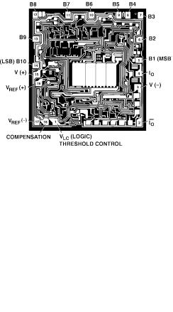
DICE CHARACTERISTICS
DIE SIZE 0.091 3 0.087 inch, 7,917 sq. mils (2.311 3 2.210 mm, 5.107 sq. mm)
REV. D |
–3– |
 Loading...