


application
INFO
available
UCC2918
UCC3918
Low On Resistance Hot Swap Power Manager
FEATURES
•Integrated 0.06Ω Power MOSFET
•3V to 6V Operation
•External Analog control of Fault Current from 0A to 4A
•Independent Analog Control of Current Limit up to 5A
•Fast Overload Protection
•Uni-directional Switch
•Minimal External Components
•1µA ICC when Disabled
•Programmable On Time
•Programmable Start Delay
•Fixed 3% Duty Cycle
DESCRIPTION
The UCC3918 Low on Resistance Hot Swap Power Manager provides complete power management, hot swap capability, and circuit breaker functions. The only components needed to operate the device, other than supply bypassing, are a timing capacitor, and 2 programming resistors. All control and housekeeping functions are integrated, and externally programmable. These include the fault current level, maximum output sourcing current, maximum fault time, and startup delay. In the event of a constant fault, the internal fixed 3% duty cycle ratio limits the average output power. The IFAULT pin allows linear programming of the fault level current from 0A to 4A.
Fast overload protection is accomplished by an additional overload comparator. Its threshold is internally set above the maximum sourcing current limit setting. In the event of a short circuit or extreme current condition, this comparator is tripped, shutting down the output. This function is needed since the maximum sourcing current limit loop has a finite bandwidth.
When the output current is below the fault level, the output MOSFET is switched on with a nominal resistance of 0.06Ω. When the output current exceeds the fault level or the maximum sourcing level, the output remains on, but the fault timer starts charging CT. Once CT charges to a preset threshold, the switch is turned off, and remains off for 30 times the programmed fault time. When the output current reaches the maximum sourcing level, the MOSFET transitions form a switch to a constant current source.
BLOCK DIAGRAM |
|
|
|
|
|
|
(continued) |
|
|
|
|
|
|
|
|
||
|
|
CHARGE |
|
|
|
|
1 |
VIN |
|
|
PUMP |
|
|
|
|
|
|
|
|
|
|
|
|
|
|
|
|
OVERLOAD |
REVERSE |
+ |
20mV |
|
2 |
VIN |
|
|
COMPARATOR |
COMPARATOR |
|
|
|
|||
|
|
|
|
|
|
|||
|
|
|
|
|
|
|
3 |
VIN |
|
|
|
|
|
|
|
|
|
|
+ |
|
|
VOUT |
CURRENT SENSE |
|
|
|
|
|
|
|
|
|
|
||
IMAX |
9 |
|
|
|
H = OPEN |
|
|
|
|
|
|
|
|
|
|
||
|
MAXIMUM |
|
|
|
|
|
|
|
|
CURRENT |
|
|
|
|
|
|
|
|
LEVEL |
OVERCURRENT |
|
|
|
|
|
|
|
CURRENT |
ON TIME |
|
|
|
14 |
VOUT |
|
|
COMPARATOR |
|
|
|
||||
|
|
|
|
|
|
|||
|
FAULT LEVEL |
|
CONTROL |
|
|
|
15 |
VOUT |
|
|
|
|
|
|
|
||
IFAULT |
8 |
|
3% DUTY |
|
|
|
|
|
|
|
|
|
|
|
16 |
VOUT |
|
|
|
|
CYCLE |
THERMAL |
|
|||
|
|
|
|
SHUTDOWN |
|
|
|
|
|
|
|
|
|
|
|
1.5V |
|
|
|
|
|
INTERNAL |
+ |
|
|
|
|
|
|
|
|
BIAS |
– |
7 |
SHTDWN |
|
|
|
|
|
|
|||
5 |
4 |
13 |
12 |
10 |
6 |
GND |
HEAT SINK GND |
CT |
FAULT |
|
|
PINS |
|
|
UDG-99153 |
SLUS384A - NOVEMBER 1999
DESCRIPTION (continued)
The UCC3918 is designed for unidirectional current flow, emulating an ideal diode in series with the power switch. This feature is particularly attractive in applications where many devices are powering a common bus, such as with SCSI Termpwr. The UCC3918 can also be put into the sleep mode, drawing only 1 A of supply current.
Other features include an open drain fault output indicator, thermal shutdown, undervoltage lockout, 3V to 6V operation, and a low thermal resistance small outline power package.
ABSOLUTE MAXIMUM RATINGS
Input Supply Voltage (VIN) . . . . . . . . . . . . . . . . . . . . . . . . . . 8V SOIC Power Dissipation . . . . . . . . . . . . . . . . . . . . . . . . . . 2.5W Fault Output Sink Current. . . . . . . . . . . . . . . . . . . . . . . . . 50mA Fault Output Voltage . . . . . . . . . . . . . . . . . . . . . . . . . . . . . . VIN Output Current (DC) . . . . . . . . . . . . . . . . . . . . Internally Limited Input Voltage
SHTDWN, IFAULT, IMAX . . . . . . . . . . . . . . . . . –0.3V to VIN Storage Temperature Range . . . . . . . . . . . . . –65°C to +150°C Operating Junction Temperature Range . . . . –55°C to +150°C Lead Temperature (Soldering, 10 sec.) . . . . . . . . . . . . . +300°C
Unless otherwise indicated, voltages are reference to ground and currents are positive into, negative out of the specified terminal. Pulsed is defined as a less than 10% duty cycle with a maximum duration of 500 S. Consult Packaging Section of Databook for thermal limitations and considerations of package.
UCC2918
UCC3918
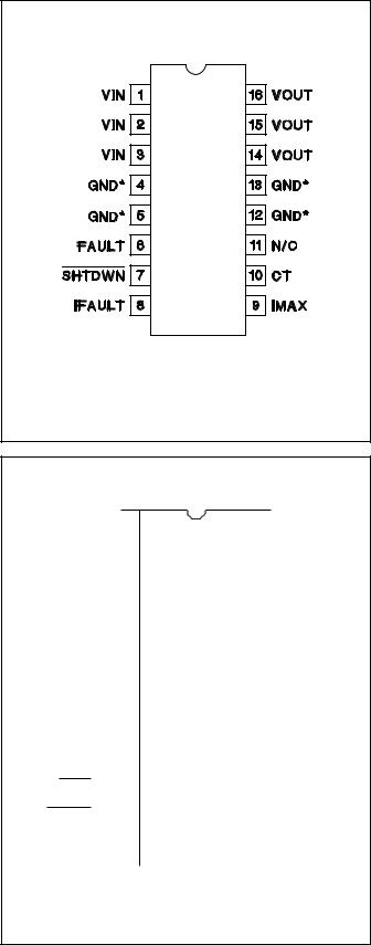
CONNECTION DIAGRAM
DIL-16, SOIC-16 (Top View)
N Package, DP Package
* Pin 5 serves as the lowest impedance to the electrical ground. Pins 4, 12, and 13 serve as heat sink/ground. These pins should be connected to large etch PCB areas to help dissipate heat. For N Package, pins 4, 12, and 13 are N/C.
TSSOP-24 (Top View)
PWP Package
|
|
|
|
|
VIN |
1 |
|
24 |
VOUT |
|
|
|
|
|
|
|
|
|
|
VIN |
2 |
|
23 |
VOUT |
|
|
|
|
|
|
|
|
|
|
VIN |
3 |
|
22 |
VOUT |
|
|
|
|
|
|
|
|
|
|
VIN |
4 |
|
21 |
VOUT |
|
|
|
|
|
|
|
|
|
|
GND* |
5 |
|
20 |
GND* |
|
|
|
|
|
|
|
|
|
|
GND* |
6 |
|
19 |
GND* |
|
|
|
|
|
|
|
|
|
|
GND* |
7 |
|
18 |
GND* |
|
|
|
|
|
|
|
|
|
|
GND* |
8 |
|
17 |
GND* |
|
|
|
|
|
|
|
|
|
|
GND* |
9 |
|
16 |
GND* |
FAULT |
|
|
|
|
|
|
|
|
|
10 |
|
15 |
N/C |
|
|
|
|
|
|
|
|
|
|
|
SHTDWN |
11 |
|
14 |
CT |
|
|
|
|
|
|
|
|
|
|
IFAULT |
12 |
|
13 |
IMAX |
|
|
|
|
|
|
|
|
|
|
* Pin 9 serves as the lowest impedance to the electrical ground. Pins 5, 6, 7, 8, 16, 17, 18, 19 and 20 serve as heat sink/ground.
2

UCC2918
UCC3918
ELECTRICAL CHARACTERISTICS: Unless otherwise specified, TA = 0°C to 70°C for the UCC3918, –40°C to 85° for the UCC2918, VIN = 5V. RIMAX = 42.2k, RIFAULT = 52.3k, SHTDWN = 2.4. TA = TJ.
PARAMETER |
|
|
TEST CONDITIONS |
MIN |
TYP |
MAX |
UNITS |
||
Supply Section |
|
|
|
|
|
|
|
|
|
Voltage Input Range, VIN |
|
|
|
|
|
3 |
5 |
6 |
V |
VDD Supply Current |
|
No Load |
|
1 |
2 |
mA |
|||
|
|
|
|
|
|
|
|
|
µA |
Sleep Mode Current |
|
SHTDWN = 0.2V |
|
0.5 |
5 |
||||
Output Section |
|
|
|
|
|
|
|
|
|
RDSON |
|
IOUT = 1A to 4A, VIN = 5V, TA = 25°C |
|
0.075 |
0.095 |
Ω |
|||
|
|
IOUT = 1A to 4A, VIN = 3V, TA = 25°C |
|
0.09 |
0.116 |
Ω |
|||
|
|
IOUT = 1A to 4A, VIN = 5V |
|
0.75 |
0.125 |
Ω |
|||
|
|
IOUT = 1A to 4A, VIN = 3V |
|
0.09 |
0.154 |
Ω |
|||
|
|
|
|
|
|
|
|
|
|
Reverse Leakage Current |
|
VIN = 0V, VOUT = 5V, SHTDWN = 0V |
|
|
20 |
A |
|||
Initial Startup Time |
|
(Note 1) |
|
100 |
|
µS |
|||
Thermal Shutdown |
|
(Note 1) |
|
170 |
|
DEG |
|||
Output Section (cont) |
|
|
|
|
|
|
|
|
|
Thermal Hysteresis |
|
(Note 1) |
|
10 |
|
DEG |
|||
|
|
|
|
|
|
|
|
|
µA |
Output Leakage |
|
SHTDWN = 0.2V |
|
|
20 |
||||
Trip Current |
|
RIFAULT = 105k |
0.75 |
1 |
1.25 |
A |
|||
|
|
RIFAULT = 52.3k |
1.7 |
2 |
2.3 |
A |
|||
|
|
RIFAULT = 34.8k |
2.5 |
3 |
3.5 |
A |
|||
|
|
RIFAULT = 25.5k |
3.3 |
4 |
4.7 |
A |
|||
Maximum Output Current |
|
RIMAX = 118k |
0.3 |
1 |
1.7 |
A |
|||
|
|
RIMAX = 60.4k |
1 |
2 |
3 |
A |
|||
|
|
RIMAX = 42.2k |
2 |
3 |
4 |
A |
|||
|
|
RIMAX = 33.2k |
2.5 |
3.8 |
5.1 |
A |
|||
|
|
RIMAX = 27.4k |
3.0 |
4.6 |
6.2 |
A |
|||
Fault Section |
|
|
|
|
|
|
|
|
|
CT Charge Current |
|
VCT = 1V |
–50 |
–36 |
–22 |
µA |
|||
CT Discharge Current |
|
VCT = 1V |
0.5 |
1.2 |
2.0 |
µA |
|||
Fault Section (cont.) |
|
|
|
|
|
|
|
|
|
Output Duty Cycle |
|
VOUT = 0V |
1.5 |
3 |
6 |
% |
|||
CT Fault Threshold |
|
|
|
|
|
0.8 |
1.3 |
1.8 |
V |
CT Reset Threshold |
|
|
|
|
|
0.25 |
0.5 |
0.75 |
V |
Shutdown Section |
|
|
|
|
|
|
|
|
|
Shutdown Threshold |
|
|
|
|
|
1.1 |
1.5 |
2.0 |
V |
Shutdown Hysteresis |
|
|
|
|
|
|
100 |
|
mV |
|
|
|
|
|
|
|
|
|
|
Input Low Current |
|
SHTDWN = 0V |
–500 |
0 |
500 |
nA |
|||
|
|
|
|
|
|
|
|
|
µA |
Input High Current |
|
SHTDWN = 2V |
–2 |
–1 |
–0.5 |
||||
Open Drain Fault Output |
|
|
|
|
|
|
|
|
|
High Level Output Current |
|
|
|
|
|
|
|
1 |
µA |
Low Level Output Voltage |
|
IOUT = 1mA |
|
0.4 |
0.9 |
V |
|||
Note 1: Guaranteed by design. Not 100% tested in production.
3
 Loading...