


UCC39151
15V Programmable Hot Swap Power Manager
FEATURES
∙Integrated 0.15Ω Power MOSFET
∙7V to 15V Operation
∙Digital Programmable Current Limit from 0A to 3A
∙Programmable ON Time
∙Programmable Start Delay
∙Fixed 2% Duty Cycle
∙Thermal Shutdown
∙Fault Output Indicator
∙Maximum Output Current can be set to 1A above the Programmed Fault Level or to a full 4A
∙Power SOIC and TSSOP, Low Thermal Resistance Packaging
BLOCK DIAGRAM
DESCRIPTION
The UCC39151 Programmable Hot Swap Power Manager provides complete power management, hot swap capability, and circuit breaker functions. The only external component required to operate the device, other than power supply bypassing, is the fault timing capacitor, CT. All control and housekeeping functions are integrated, and externally programmable. These include the fault current level, maximum output sourcing current, maximum fault time, and startup delay. In the event of a constant fault, the Internal fixed 2% duty cycle ratio limits average output power.
The internal 4 bit DAC allows programming of the fault level current from 0A to 3A with 0.25A resolution. The IMAX control pin sets the maximum sourcing current to 1A above the trip level or to a full 4A of output current for fast output capacitor charging.
When the output current is below the fault level, the output MOSFET is switched ON with a nominal ON resistance of 0.15Ω. When the output current exceeds the fault level, but is less than the maximum sourcing level, the output remains switched ON, but the fault timer starts, charging CT. Once CT charges to a preset threshold, the switch is turned OFF, and remains OFF for 50 times the programmed fault time. When the output current reaches the maximum sourcing level, the MOSFET transitions from a switch to a constant current source.
(continued)
Note: Pin numbers refer to DIL-16 and SOIC-16 packages.
02/99
UDG-94136-3
ABSOLUTE MAXIMUM RATINGS
VIN . . . . . . . . . . . . . . . . . . . . . . . . . . . . . . . . . . . . . . +15.5 Volts VOUT VIN. . . . . . . . . . . . . . . . . . . . . . . . . . . . . . . . . . . . .0.3V FAULT Sink Current . . . . . . . . . . . . . . . . . . . . . . . . . . . . . 50mA FAULT Voltage . . . . . . . . . . . . . . . . . . . . . . . . . . . . . 0.3 to 8V Output Current . . . . . . . . . . . . . . . . . . . . . . . . . . . . Self Limiting
TTL Input Voltage . . . . . . . . . . . . . . . . . . . . . . . . . . 0.3 to VIN Storage Temperature . . . . . . . . . . . . . . . . . . . 65 C to +150
 C
C
Junction Temperature . . . . . . . . . . . . . . . . . . . 55 C to +150
 C Lead Temperature (Soldering, 10 sec.) . . . . . . . . . . . . . +300
 C
C
Currents are positive into, negative out of the specified terminal. Consult Packaging Section of Databook for thermal limitations and considerations of packages.
UCC39151
DESCRIPTION (cont.)
The UCC39151 can be put into sleep mode, drawing only 20mA of supply current. Other features include an open drain Fault Output Indicator, Thermal Shutdown, Undervoltage Lockout, 7V to 15V operation, and low thermal resistance SOIC and TSSOP Power Packages.
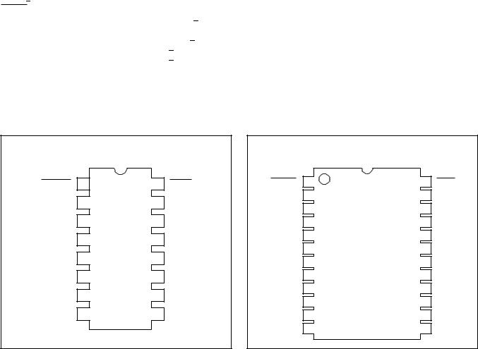
CONNECTION DIAGRAMS
DIL-16, SOIC-16 (Top View)
N, DP Package
SHTDWN |
1 |
16 |
FAULT |
VIN |
2 |
15 |
VOUT |
VIN |
3 |
14 |
VOUT |
GND* |
4 |
13 |
GND* |
EGND* |
5 |
12 |
GND* |
B3 |
6 |
11 |
CT |
B2 |
7 |
10 |
IMAX |
B1 |
8 |
9 |
B0 |
*Pin 5 serves as lowest impedance to the electrical ground; Pins 4, 12, and 13 serve as heat sink/ground. These pins should be connected to large etch areas to help dissipate heat. For N Package, pins 4, 12, and 13 are N/C.
PWP-24 (Top View)
TSSOP Package
SHTDWN |
1 |
24 |
FAULT |
VIN |
2 |
23 |
VOUT |
VIN |
3 |
22 |
VOUT |
N/C |
4 |
21 |
N/C |
GND* |
5 |
20 |
GND* |
GND* |
6 |
19 |
GND* |
GND* |
7 |
18 |
GND* |
GND* |
8 |
17 |
GND* |
EGND* |
9 |
16 |
N/C |
B3 |
10 |
15 |
CT |
B2 |
11 |
14 |
IMAX |
B1 |
12 |
13 |
B0 |
*Pin 9 serves as lowest impedance to the electrical ground; other GND pins serve as heat sink/ground. These pins should be connected to large etch areas to help dissipate heat.
ELECTRICAL CHARACTERISTICS Unless otherwise stated, these specifications apply for TA = 0°C to 70°C for the UCC39151, VIN = 12V, IMAX = 0.4V, SHTDWN = 2.4V, TA = TJ.
PARAMETER |
|
TEST CONDITIONS |
MIN |
TYP |
MAX |
UNITS |
|
Supply Section |
|
|
|
|
|
|
|
Voltage Input Range |
|
|
|
7.0 |
|
15.0 |
V |
Supply Current |
|
|
|
|
1.0 |
2.0 |
mA |
|
|
|
|
|
|
|
μA |
Sleep Mode Current |
|
SHTDWN = 0.2V, No load |
|
100 |
150 |
||
|
|
|
|
|
|
|
|
Output Leakage |
|
SHTDWN = 0.2V |
|
|
20 |
mA |
|
Output Section |
|
|
|
|
|
|
|
Voltage Drop |
|
IOUT = 1A (10V to 12V) |
|
0.15 |
0.3 |
V |
|
|
|
IOUT = 2A (10V to 12V) |
|
0.3 |
0.6 |
V |
|
|
|
IOUT = 3A (10V to 12V) |
|
0.45 |
0.9 |
V |
|
|
|
IOUT = 1A, VIN = 7V and 15V |
|
0.2 |
0.4 |
V |
|
|
|
IOUT = 2A, VIN = 7V and 15V |
|
0.4 |
0.8 |
V |
|
|
|
IOUT = 3A, VIN = 7V, 12V Max. |
|
0.6 |
1.2 |
V |
|
2
 Loading...