


Fairchild Semiconductor 100324SCX, 100324QIX, 100324QI, 100324QCX, 100324QC Datasheet
...
July 1988
Revised August 2000
100324
Low Power Hex TTL-to-ECL Translator
General Description
The 100324 is a hex translator, designed to convert TTL logic levels to 100K ECL logic levels. The inputs are compatible with standard or Schottky TTL. A common Enable (E), when LOW, holds all inverting outputs HIGH and holds all true outputs LOW. The differential outputs allow each circuit to be used as an inverting/non-inverting translator, or as a differential line driver. The output levels are voltage compensated over the full − 4.2V to − 5.7V range.
When the circuit is used in the differential mode, the 100324, due to its high common mode rejection, overcomes voltage gradients between the TTL and ECL ground systems. The VEE and VTTL power may be applied in either order.
The 100324 is pin and function compatible with the 100124 with similar AC performance, but features power dissipation roughly half of the 100124 to ease system cooling requirements.
Features
■Pin/function compatible with 100124
■Meets 100124 AC specifications
■50% power reduction of the 100124
■Differential outputs
■2000V ESD protection
■− 4.2V to − 5.7V operating range
■Available to MIL-STD-883
■Available to industrial grade temperature range (PLCC package only)
Ordering Code:
Order Number |
Package Number |
Package Description |
|
|
|
100324SC |
M24B |
28-Lead Small Outline Integrated Circuit (SOIC), JEDEC MS-013, 0.300 Wide |
|
|
|
100324PC |
N24E |
24-Lead Plastic Dual-In-Line Package (PDIP), JEDEC MS-010, 0.400 Wide |
|
|
|
100324QC |
V28A |
28-Lead Plastic Lead Chip Carrier (PLCC), JEDEC MO-047, 0.450 Square |
|
|
|
100324QI |
V28A |
28-Lead Plastic Lead Chip Carrier (PLCC), JEDEC MO-047, 0.450 Square |
|
|
Industrial Temperature Range (− 40° C to + 85° C) |
|
|
|
Devices also available in Tape and Reel. Specify by appending the suffix letter “X” to the ordering code.
Connection Diagrams
24-Pin DIP/SOIC 28-Pin PLCC
Translator ECL-to-TTL Hex Power Low 100324
© 2000 Fairchild Semiconductor Corporation |
DS009878 |
www.fairchildsemi.com |
100324
Pin Descriptions |
Truth Table |
|
|
|
|
|
|||||||||
|
|
|
|
|
|
|
|
|
|
|
|
|
|||
|
|
Pin Names |
Description |
|
|
Inputs |
|
Outputs |
|||||||
|
|
|
|
|
|
|
|
|
|
|
|
|
|||
|
|
D0–D5 |
Data Inputs |
|
D |
n |
|
E |
Q |
Q |
|||||
|
|
E |
Enable Input |
|
|
|
n |
|
n |
||||||
|
|
|
X |
|
L |
L |
|
H |
|||||||
|
|
Q0–Q5 |
Data Outputs |
|
|
|
|||||||||
|
|
|
|
|
|
|
|
|
|||||||
|
|
|
L |
|
H |
L |
|
H |
|||||||
|
|
|
|
|
|
|
|
|
|
|
|
|
|
|
|
|
|
Q |
0–Q |
5 |
Complementary |
|
|
|
|
|
|
|
|||
|
|
|
H |
|
H |
H |
|
L |
|||||||
|
|
|
|
|
|
Data Outputs |
|
|
|
|
|
|
|
|
|
|
|
|
|
|
|
H = HIGH Voltage Level |
|
|
|
|
|
||||
|
|
|
|
|
|
|
|
|
|
|
|
||||
|
|
|
|
|
|
|
L = LOW Voltage Level |
|
|
|
|
|
|||
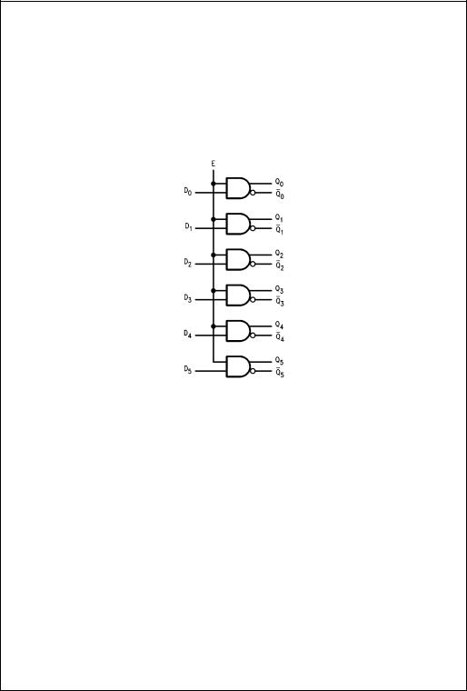
Logic Diagram
www.fairchildsemi.com |
2 |

Absolute Maximum Ratings(Note 1)
Storage Temperature (TSTG) |
− 65° C to + 150° C |
Maximum Junction Temperature (TJ) |
+ 150° C |
VEE Pin Potential to Ground Pin |
− 7.0V to + 0.5V |
VTTL Pin Potential to Ground Pin |
− 0.5V to + 6.0V |
Input Voltage (DC) |
− 0.5V to + 6.0V |
Output Current (DC Output HIGH) |
− 50 mA |
ESD (Note 2) |
≥ 2000V |
Recommended Operating
Conditions
Case Temperature (TC) |
|
Commercial |
0° C to + 85° C |
Industrial |
− 40° C to + 85° C |
Supply Voltage (VEE) |
− 5.7V to − 4.2V |
Note 1: The “Absolute Maximum Ratings” are those values beyond which the safety of the device cannot be guaranteed. The device should not be operated at these limits. The parametric values defined in the Electrical Characteristics tables are not guaranteed at the absolute maximum rating. The “Recommended Operating Conditions” table will define the conditions for actual device operation.
Note 2: ESD testing conforms to MIL-STD-883, Method 3015.
Commercial Version
DC Electrical Characteristics (Note 3)
VEE = − 4.2V to − 5.7V, VCC = VCCA = |
GND, TC = 0° C to + 85° C, VTTL = + 4.5V to + 5.5V |
|
|
|
|
|
|
|||||
Symbol |
Parameter |
|
Min |
Typ |
Max |
Units |
|
|
Conditions |
|
||
|
|
|
|
|
|
|
|
|
|
|
|
|
VOH |
Output HIGH Voltage |
|
− 1025 |
− 955 |
− 870 |
mV |
VIN = |
VIH (Max) |
|
|
Loading with |
|
VOL |
Output LOW Voltage |
|
− 1830 |
− 1705 |
− 1620 |
or VIL (Min) |
|
|
50Ω |
to − 2.0V |
||
|
|
|
|
|||||||||
VOHC |
Output HIGH Voltage |
|
− 1035 |
|
|
mV |
VIN = |
VIH(Min) |
|
|
Loading with |
|
VOLC |
Output LOW Voltage |
|
|
|
− 1610 |
or VIL (Max) |
|
|
50Ω |
to − 2.0V |
||
|
|
|
|
|
|
|||||||
VIH |
Input HIGH Voltage |
|
2.0 |
|
5.0 |
V |
Guaranteed HIGH |
|
|
|
||
|
|
|
|
|
|
|
Signal for All Inputs |
|
|
|
||
|
|
|
|
|
|
|
|
|
|
|
||
VIL |
Input LOW Voltage |
|
0 |
|
0.8 |
V |
Guaranteed LOW |
|
|
|
||
|
|
|
|
|
|
|
Signal for All Inputs |
|
|
|
||
|
|
|
|
|
|
|
|
|
|
|
|
|
VCD |
Input Clamp Diode Voltage |
|
− 1.2 |
|
|
V |
IIN = |
− 18 mA |
|
|
|
|
IIH |
Input HIGH Current |
|
|
|
|
|
VIN = |
+ 2.4V, |
|
|
|
|
|
Data |
|
|
|
20 |
µ A |
All Other Inputs VIN = |
GND |
|
|||
|
Enable |
|
|
|
120 |
|
|
|
|
|
|
|
|
|
|
|
|
|
|
|
|
|
|
|
|
|
Input HIGH Current |
|
|
|
1.0 |
mA |
VIN = |
+ 5.5V, |
|
|
|
|
|
Breakdown Test, All Inputs |
|
|
|
All Other Inputs = GND |
|
||||||
|
|
|
|
|
|
|
||||||
|
|
|
|
|
|
|
|
|
|
|
|
|
IIL |
Input LOW Current |
|
|
|
|
|
VIN = |
+ 0.4V, |
|
|
|
|
|
Data |
|
− 0.9 |
|
|
mA |
All Other Inputs VIN = |
VIH |
|
|||
|
Enable |
|
− 5.4 |
|
|
|
|
|
|
|
|
|
|
|
|
|
|
|
|
|
|
|
|
|
|
IEE |
VEE Power Supply Current |
|
− 70 |
− 45 |
− 22 |
mA |
All Inputs VIN = |
+ 4.0V |
|
|
|
|
ITTL |
VTTL Power Supply Current |
|
|
25 |
38 |
mA |
All Inputs VIN = |
GND |
|
|
|
|
Note 3: The specified limits represent the “worst case” value for the parameter. Since these values normally occur at the temperature extremes, additional noise immunity and guardbanding can be achieved by decreasing the allowable system operating ranges. Conditions for testing shown in the tables are chosen to guarantee operation under “worst case” conditions.
DIP AC Electric Characteristics
VEE = − 4.2V to − 5.7V, VCC = VCCA = GND, VTTL = |
+ 4.5V to + 5.5V |
|
|
|
|
|
||||
Symbol |
Parameter |
TC = 0° C |
TC = + 25° C |
TC = + 85° C |
Units |
Conditions |
||||
Min |
Max |
Min |
Max |
Min |
Max |
|||||
|
|
|
|
|||||||
|
|
|
|
|
|
|
|
|
|
|
tPLH |
Propagation Delay |
0.50 |
3.00 |
0.50 |
2.90 |
0.50 |
3.00 |
ns |
|
|
tPHL |
Data and Enable to Output |
Figures 2, 1 |
||||||||
|
|
|
|
|
|
|
||||
tTLH |
Transition Time |
0.45 |
1.80 |
0.45 |
1.80 |
0.45 |
1.80 |
ns |
|
|
tTHL |
20% to 80%, 80% to 20% |
|
||||||||
|
|
|
|
|
|
|
|
|||
100324
3 |
www.fairchildsemi.com |
 Loading...