


Texas Instruments UCC39422PWTR, UCC39422PW, UCC39422N, UCC39421PWTR, UCC39421PW Datasheet
...Multimode High Frequency PWM Controller
UCC29421/2
UCC39421/2
PRELIMINARY
FEATURES |
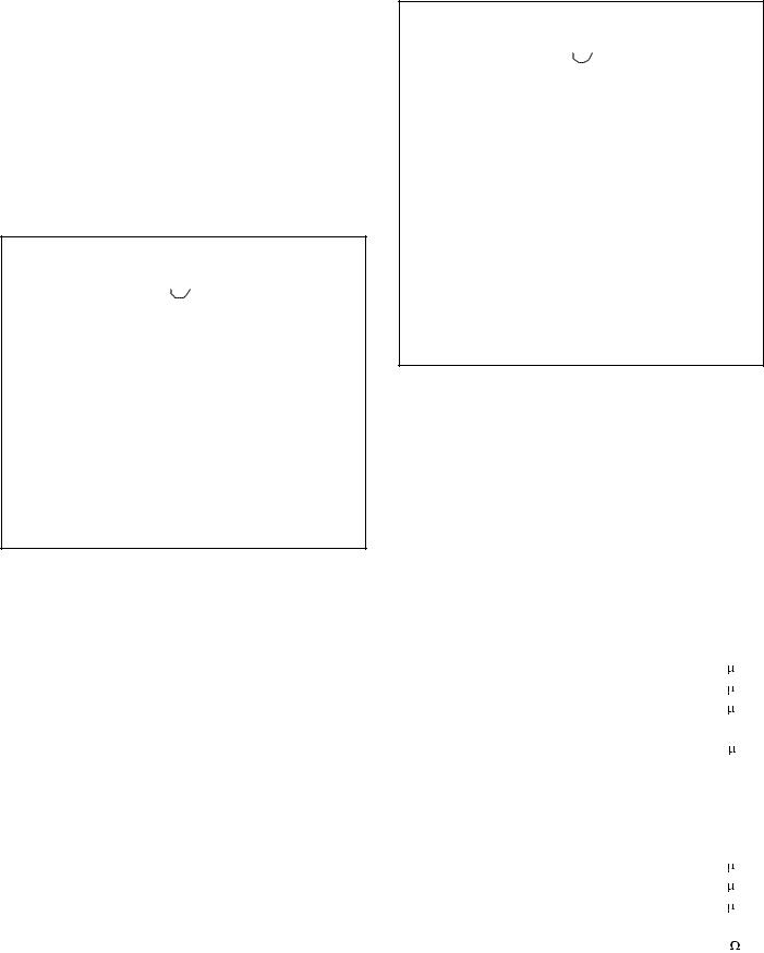
SIMPLIFIED BLOCK DIAGRAM AND APPLICATION CIRCUIT |
|||||||
• Operation Down to an Input Voltage |
|
|
|
|
|
|
|
|
of 1.8V |
|
|
|
|
|
|
|
|
• High Efficiency Boost or Flyback |
|
|
|
|
|
1.8VMIN |
|
|
|
|
|
|
|
|
+ |
|
|
(Buck-Boost) Topologies |
|
|
VPUMP |
|
VIN |
2 CELL |
||
|
|
|
|
|||||
|
|
7 |
|
9 |
|
|
ALKALINE/ |
|
|
|
|
|
|
|
|||
|
|
|
|
|
|
NiCd OR |
||
• Drives External FETs for High Current |
|
|
|
|
|
|
+ |
|
|
|
1.25V |
|
|
|
1 LI-ION |
||
|
|
|
|
|
|
|||
Applications |
|
|
VREF |
|
|
|
CP |
|
|
|
|
|
|
8 |
|
||
|
|
|
|
|
|
|
||
• Up to 2MHz Oscillator |
SYNC/SD |
13 |
|
CHARGE |
|
|
||
|
|
PUMP |
3 |
VOUT |
|
|||
|
|
PWM |
|
|
|
|
||
|
RT |
|
|
|
|
|
|
|
• Synchronizable Fixed Frequency |
14 |
OSC |
|
|
|
|
|
|
|
|
|
|
RSEN |
|
|||
|
|
|
|
2 |
VOUT |
|||
|
|
|
|
|
|
|||
Operation |
|
|
|
VPUMP |
|
|
||
|
|
LP_MODE |
|
|
RECT |
|
||
|
|
|
|
|
|
4 |
|
|
• High Efficiency Low Power Mode |
|
|
|
|
|
|
|
|
|
|
|
|
|
|
RSEL |
|
|
|
|
|
ANTI- |
|
|
19 |
|
|
• High Efficiency at Very Low Power |
|
|
|
|
|
|
||
|
|
CROSS |
|
|
|
|
||
|
|
|
|
|
|
|
||
|
|
COND. |
VGD |
|
|
CHRG |
|
|
with Programmable Variable |
|
|
|
|
|
|||
|
|
|
|
|
6 |
|
||
|
|
|
|
|
|
|
||
Frequency Mode |
|
|
|
|
|
|
|
|
• Pulse by Pulse Current Limit |
|
|
PWM CIRCUITRY |
|
|
12 |
ISENSE |
|
|
|
CURRENT LIMIT |
+ |
|
|
|
||
|
|
|
|
|
50mV TYP |
|
||
|
|
|
|
X10 |
|
|
|
|
• 5 A Supply Current in Shutdown |
|
|
LOW POWER |
– |
|
5 |
PGND |
|
|
|
|
|
|
|
|||
|
|
|
MODE |
ERROR |
1.25V |
|
|
|
• 150 A Supply Current in Sleep Mode |
|
|
|
|
|
|||
|
|
|
|
|
|
|
||
|
|
SLOPE |
AMP |
|
|
|
|
|
|
|
|
COMPENSATION |
+ |
|
|
FB |
|
• Selectable NMOS or PMOS |
|
|
|
– |
|
17 |
|
|
|
|
PFM MODE |
|
|
|
|||
|
|
|
|
|
COMP |
|
||
Rectification |
|
|
CONTROL |
|
|
18 |
|
|
|
|
|
|
|
|
|||
|
|
|
|
|
|
|
|
|
• Built-in Power on Reset |
|
|
|
|
|
16 |
PFM |
|
GND |
|
|
|
|
|
|
||
15 |
|
|
|
|
|
|
||
(UCC39422 Only) |
|
|
– |
|
|
|
|
|
|
|
|
|
|
|
|
|
|
|
|
|
|
+ |
|
|
|
|
• Built-in Low Voltage Detect |
|
|
|
1.23/1.25V |
|
|
||
(UCC39422 Only) |
RESET |
|
|
UCC39422 |
|
|
|
|
|
1 |
|
|
|
|
|||
|
|
|
|
|
|
|||
|
|
200mS |
ONLY |
|
|
|
|
|
|
|
|
|
|
|
|
||
|
|
|
RESET/ |
– |
|
|
|
|
|
|
|
POR |
+ |
|
1.18V |
|
|
|
|
|
|
|
RSADJ |
|
||
|
LOWBAT |
|
|
|
|
20 |
|
|
|
|
|
|
|
|
|
||
|
|
10 |
|
|
|
|
|
|
|
|
|
|
|
|
VDET |
|
|
|
|
|
|
|
|
11 |
|
|
|
|
|
|
+ |
|
|
|
|
|
|
|
|
– |
|
1.25V |
|
|
|
|
|
|
|
|
|
|
UDG-98122 |
DESCRIPTION
The UCC39421 family of synchronous PWM controllers is optimized to operate from dual Alkaline/NiCd cells or a single Lithium-Ion (Li-Ion) cell, and convert to adjustable output voltages from 2.5V to 8V. For applications where the input voltage does not exceed the output, a standard boost configuration is utilized. For other applications where the input voltage can swing above and below the output, a 1:1 coupled-inductor (Flyback or SEPIC) is used in place of the single inductor. Fixed frequency operation can be programmed, or synchronized to an external clock source. In applications where at light loads variable frequency mode is acceptable, the IC can be programmed to automatically enter PFM (Pulse Frequency Modulation) mode for an additional efficiency benefit.
SLUS246A - OCTOBER 1999
Synchronous rectification provides excellent efficiency at high power levels, where N or P type MOSFETs can be used. At lower power levels (10-20% of full load) where fixed frequency operation is required, Low Power Mode is entered. This mode optimizes efficiency by cutting back on the gate drive of the charging FET. At very low power levels, the IC enters a variable frequency mode (PFM). PFM can be disabled by the user.
Other features include pulse by pulse current limiting, and a low 5 A quiescent current during shutdown. The UCC39422 incorporates programmable Power on Reset circuitry and an uncommitted comparator for low voltage detection. The available packages are 20 pin TSSOP, or 20 pin N for the UCC39422, and 16 pin TSSOP, or 16 pin N for the UCC39421.
ABSOLUTE MAXIMUM RATINGS
Supply Voltage (VIN, VOUT,VPUMP) . . . . . . . . . . . . . . . . . . 8V CP . . . . . . . . . . . . . . . . . . . . . . . . . . . . . . . . . . . . . . . . . . . . . 8V RSEN. . . . . . . . . . . . . . . . . . . . . . . . . . . . . . . . . . . . –0.3 to 12V SYNC/SD. . . . . . . . . . . . . . . . . . . . . . . . . . . . . . . . . . –0.3 to 5V ISENSE . . . . . . . . . . . . . . . . . . . . . . . . . . . . . . . . . . . –0.3 to 1V Storage Temperature . . . . . . . . . . . . . . . . . . . –65°C to +150°C Junction Temperature. . . . . . . . . . . . . . . . . . . –55°C to +150°C Lead Temperature (Soldering, 10 sec.) . . . . . . . . . . . . . +300°C
All voltages are with respect to GND. Currents are positive into, negative out of the specified terminal. Consult Packaging Section of Databook for thermal limitations and considerations of packages.
TSSOP-16, DIL-16 (TOP VIEW)
N, PW Packages
RSEN |
|
|
|
|
|
|
1 |
|
|
|
16 |
RSEL |
|
VOUT |
|
|
|
|
|
|
|
|
|
|
|
|
|
2 |
|
|
|
15 |
COMP |
|
RECT |
|
|
|
|
|
FB |
|
|
|
|
|
||
3 |
|
|
|
14 |
||
PGND |
|
|
|
|
|
PFM |
|
|
|
|
|
||
4 |
|
|
|
13 |
||
CHRG |
|
|
|
|
|
GND |
|
|
|
|
|
||
5 |
|
|
|
12 |
||
VPUMP |
|
|
|
|
|
RT |
|
|
|
|
|
||
6 |
|
|
|
11 |
||
CP |
|
|
|
|
|
SYNC/SD |
|
|
|
|
|
||
7 |
|
|
|
10 |
||
VIN |
|
|
|
|
|
ISENSE |
|
|
|
|
|
||
8 |
|
|
|
9 |
||
|
|
|
|
|
|
|
|
|
|
|
|
|
|
UCC29421/2
UCC39421/2
CONNECTION DIAGRAMS
TSSOP-20, DIL-20 (TOP VIEW)
N, PW Packages
RESETB |
|
|
|
|
|
RSADJ |
1 |
|
|
|
20 |
||
|
|
|
|
|
|
RSEL |
|
|
|
|
|
|
|
RSEN |
2 |
|
|
|
19 |
|
|
|
|
|
|
|
|
|
|
|
|
|
|
|
VOUT |
3 |
|
|
|
18 |
COMP |
|
|
|
|
|
|
|
|
|
|
|
|
|
|
RECT |
4 |
|
|
|
17 |
FB |
|
|
|
|
|
|
|
|
|
|
|
|
|
|
PGND |
5 |
|
|
|
16 |
PFM |
CHRG |
|
|
|
|
|
|
|
|
|
|
|
|
|
6 |
|
|
|
15 |
GND |
|
|
|
|
|
|
|
|
|
|
|
|
|
|
|
VPUMP |
7 |
|
|
|
14 |
RT |
|
|
|
|
|
|
|
|
|
|
|
|
|
|
CP |
8 |
|
|
|
13 |
SYNC/SD |
VIN |
|
|
|
|
|
ISENSE |
|
|
|
|
|
||
9 |
|
|
|
12 |
||
|
|
|
|
|
|
|
|
|
|
|
|
|
|
LOWBAT |
10 |
|
|
|
11 |
VDET |
|
|
|
|
|
|
|
|
|
|
|
|
|
|
ELECTRICAL CHARACTERISTICS: Unless otherwise stated these specifications apply for TA = –40°C to +85°C for UCC29421/2, 0°C to +70°C for UCC39421/2; RT=100K, VVPUMP=6V, VVIN=3V
PARAMETER |
TEST CONDITIONS |
MIN |
|
MAX |
UNITS |
VIN Section |
|
|
|
|
|
Minimum Start-up Voltage |
|
|
1.5 |
1.8 |
V |
Operating Current |
Not in PFM Mode, No Load |
|
35 |
60 |
A |
Sleep Mode Current |
PFM Mode, No Load |
|
35 |
60 |
A |
Shutdown Supply Current |
SYNC/SD = High |
|
1.5 |
4 |
A |
Startup Frequency |
VIN = 1.8V |
60 |
120 |
190 |
kHz |
Startup Off Time |
VIN = 1.8V |
|
2 |
5 |
s |
Startup CS Threshold |
VIN = 1.8V |
|
36 |
56 |
mV |
Minimum PUMP or VOUT Voltage to Exit |
|
2.2 |
2.5 |
2.8 |
V |
Startup |
|
|
|
|
|
VPUMP Section |
|
|
|
|
|
Regulation Voltage |
VVOUT=3.3V |
5.5 |
|
6.6 |
V |
Operating Current |
Outputs OFF |
|
100 |
275 |
A |
Sleep Mode Current |
|
|
5 |
15 |
A |
Shutdown Supply Current |
SYNC/SD = High, VOUT = 3V, VVPUMP = 3V |
|
2 |
15 |
A |
CP Voltage to Turn On Pump Switch |
VVPUMP = 5V |
|
5.3 |
5.5 |
V |
Pump Switch RDSON |
|
|
4 |
|
|
2

UCC29421/2
UCC39421/2
ELECTRICAL CHARACTERISTICS: Unless otherwise stated these specifications apply for TA = –40°C to +85°C for UCC29421/2, 0°C to +70°C for UCC39421/2; RT=100K, VVPUMP=6V, VVIN=3V
PARAMETER |
TEST CONDITIONS |
MIN |
|
MAX |
UNITS |
VOUT Section |
|
|
|
|
|
Operating Current |
|
|
500 |
650 |
A |
Sleep Mode Current |
|
50 |
100 |
150 |
A |
Shutdown Supply Current |
SYNC/SD = High |
|
1 |
2.2 |
A |
VPUMP to VOUT Threshold to Enable |
VOUT = 3.3V |
1.4 |
1.7 |
2.0 |
V |
N-Channel Rectifier |
|
|
|
|
|
Error Amp Section |
|
|
|
|
|
Regulation Voltage |
2V < VIN < 5V |
1.21 |
1.24 |
1.27 |
V |
FB Input Current |
VFB = 1.25V |
|
100 |
350 |
nA |
Max Sinking Current, IOL |
VCOMP = 1V, VFB = Regulation Voltage +50mV |
6.5 |
13 |
20 |
A |
Max Sourcing Current, IOH |
VCOMP = 0V, VFB = Regulation Voltage –50mV |
–20 |
–13 |
–6.5 |
A |
Transconductance |
VFB = Regulation Voltage ±4mV |
150 |
270 |
370 |
S |
Unity Gain Bandwidth |
CC = 330pF |
|
100 |
|
kHz |
Max Output Voltage |
VFB = 0V |
|
1.9 |
2.3 |
V |
Oscillator Section |
|
|
|
|
|
Frequency Stability |
RT = 350k |
100 |
150 |
190 |
kHz |
|
RT = 100k |
375 |
475 |
575 |
kHz |
|
RT = 35k |
0.9 |
1.2 |
1.4 |
MHz |
RT Voltage |
|
0.600 |
0.625 |
0.650 |
V |
SYNC Threshold |
|
0.9 |
1.2 |
1.6 |
V |
SYNC Input Current |
SYNC/SD = 2.5V |
|
|
200 |
nA |
Max SYNC High Time |
To Avoid Shutdown |
11 |
20 |
29 |
s |
SYNC Range |
RT = 100k |
1.1ƒo |
|
1.5ƒo |
kHz |
Current Sense Section |
|
|
|
|
|
Gain |
|
8 |
10 |
11 |
V/V |
Overcurrent Limit Threshold |
|
|
150 |
200 |
mV |
Unity Gain Bandwidth |
|
|
25 |
|
MHz |
COMP Voltage to ISENSE Accuracy |
ISENSE = 70mV |
0.8 |
1.0 |
1.2 |
V |
PWM Section |
|
|
|
|
|
Maximum Duty Cycle |
VISENSE = 0V, VFB = 0V |
80 |
88 |
|
% |
Minimum Duty Cycle |
VFB = 1.5V |
|
|
0 |
% |
Low Power Mode VCOMP Threshold |
At COMP pin |
0.5 |
0.6 |
0.7 |
V |
Slope Compensation Accuracy |
RT = 350k, RSLOPE = 20k |
1.4 |
2.8 |
4.0 |
A/s |
Rectifier Zero Current Threshold |
RSEL = GND |
–2 |
15 |
28 |
mV |
|
RSEL = VIN |
–28 |
–15 |
2 |
mV |
RSEL Threshold |
|
0.5 |
0.9 |
1.3 |
V |
PFM Section |
|
|
|
|
|
PFM Disable Threshold |
|
0.17 |
0.22 |
0.27 |
V |
Comp Hold During Sleep |
VPFM = 0.4 |
|
0.45 |
|
V |
Startup Delay After Sleep |
VFB < 1.23V |
|
4 |
9 |
s |
FB Voltage to Sleep Off |
|
1.19 |
1.22 |
1.25 |
V |
FB Voltage to Sleep On |
|
1.22 |
1.25 |
1.28 |
V |
Low Power Mode Timer After Sleep |
|
|
250 |
450 |
s |
3
UCC29421/2
UCC39421/2
ELECTRICAL CHARACTERISTICS: Unless otherwise stated these specifications apply for TA = –40°C to +85°C for UCC29421/2, 0°C to +70°C for UCC39421/2; RT=100K, VVPUMP=6V, VVIN=3V
PARAMETER |
|
TEST CONDITIONS |
MIN |
|
MAX |
UNITS |
VGSW Drive Section |
|
|
|
|
|
|
Rise Time |
|
CO = 1nF |
|
18 |
35 |
ns |
Fall Time |
|
CO = 1nF |
|
14 |
30 |
ns |
Output High |
|
IOUT = –100mA, Respect to VPUMP |
|
0.4 |
0.65 |
V |
|
|
IOUT = –1mA, Respect to VPUMP |
|
4 |
10 |
mV |
Output Low |
|
IOUT = 100mA |
|
0.2 |
0.35 |
V |
|
|
IOUT = 1mA |
|
2 |
6 |
mV |
Charge Off to Rectifier On Delay |
|
|
10 |
30 |
50 |
ns |
RECT Drive Section |
|
|
|
|
|
|
Rise Time |
|
CO = 1nF |
|
20 |
40 |
ns |
Fall Time |
|
CO = 1nF |
|
14 |
30 |
ns |
Output High |
|
IOUT = –100mA, Respect to VPUMP |
|
0.2 |
0.5 |
V |
|
|
IOUT = –1mA, Respect to VPUMP |
|
5 |
10 |
mV |
Output Low Rectifier |
|
IOUT = 100mA |
|
0.2 |
0.35 |
V |
|
|
IOUT = 1mA |
|
2 |
6 |
mV |
Rectifier Off to Charge On Delay |
|
|
10 |
20 |
50 |
ns |
RESET Section (UCC39422 Only) |
|
|
|
|
|
|
Reset Timeout |
|
CRSADJ = 0.33 F |
100 |
250 |
400 |
ms |
Reset Threshold |
|
% Below Regulation Voltage |
–7 |
–5.5 |
–4 |
% |
Output Low Voltage |
|
Reset Condition, I = 5mA |
|
0.1 |
0.25 |
V |
Output Leakage |
|
RESET = 8V |
|
0.05 |
0.2 |
A |
Voltage Detection Section (UCC39422 Only) |
|
|
|
|
|
|
Threshold Voltage |
|
|
1.18 |
1.26 |
1.34 |
V |
Output Low Voltage |
|
I = 5mA |
|
0.15 |
0.3 |
V |
Output Leakage |
|
LOWBAT = 8V |
|
0.05 |
0.25 |
A |
PIN DESCRIPTIONS
COMP: This is the output of the transconductance error amplifier. Connect the compensation components from this pin to ground.
CHRG: This is the gate drive output for the N-channel charge MOSFET. Connect it to the gate directly, or through a low value gate resistor.
CP: This is the input for the charge pump. For applications requiring a charge pump, connect this pin to the charge pump diode and flying capacitor, as shown in the applications diagram of Fig 5. For applications where no charge pump is required, this pin should be grounded.
FB: The feedback input is the inverting input to the tran sconductance error amplifier. Connect this pin to a resistive divider between VOUT and ground. The output voltage will be regulated to:
VOUT = 1.25 • |
R1 |
||
(R1 |
+ R2) |
||
|
|||
where R1 goes to GND and R2 goes to VOUT.
GND: This is the signal ground pin for the device. It should be tied to the local ground plane.
ISENSE: This is the input to the X10 wide bandwidth current sense amplifier. Connect this pin to the high side of the current sense resistor. An internal current is sourced out this pin for slope compensation. For applications requiring slope compensation (or filtering of the current sense signal), use a resistor in series with this pin.
LOWBAT: This is the open drain output of the uncommitted comparator. (UCC39422 only). This output is low when the VDET pin is above 1.25V.
4

PIN DESCRIPTIONS (cont.)
PFM: This is the programming pin for the PFM (Pulse Frequency Modulation) Mode threshold. Connect this pin to a resistive divider off of the FB pin (or VOUT) to set the PFM threshold. To disable PFM Mode, connect this pin to ground (below 0.2V).
PGND: This is the power ground pin for the device. Connect it directly to the ground return of the current sense resistor.
RECT: This is the gate drive output for the synchronous rectifier. Connect it to the gate of the P or N channel MOSFET directly, or through a low value gate resistor.
RECTSEN: This pin is used to sense the voltage across the synchronous rectifier for commutation. In boost configurations, connect this pin through a 1K resistor to the junction of the two MOSFETs and the inductor. In flyback and SEPIC configurations, connect this pin through a 1K resistor to the junction of the drain of the synchronous rectifier and the secondary side winding of the coupled inductor.
RSADJ: A capacitor from this pin to ground sets the reset delay. (UCC39422 only)
RSEL: This pin programs the device for N channel or P channel synchronous rectifiers by inverting the phase of the RECT gate drive output. Connect this pin to ground for N-channel MOSFETs, connect it to VIN for P-channel MOSFETs.
RESET: This is the open drain output of the Reset comparator. (UCC39422 only) and is active low.
UCC29421/2
UCC39421/2
RT: A resistor from this pin to ground programs the frequency of the pulse width modulator.
SYNC/SD: This dual function pin is the SYNC and Shutdown input. To synchronize the internal clock to an external source, this pin must be driven above 2.0V. The clock syncs to the rising edge of the input. To shutdown the converter, this pin must be held high (above 2.0V) for a minimum of 20 sec. If not used, this pin should be grounded.
VPUMP: This is the output of the charge pump. For applications requiring a charge pump, connect a 1 F capacitor from this pin to ground. Otherwise, connect this pin to the higher of VIN or VOUT, and decouple with a 0.1 F capacitor.
VOUT: Connect this pin to the output voltage. This input is used for sensing the voltage across the synchronous rectifier and for bootstrapping the gate drive to the charge FET and should be decoupled with a 0.1 F capacitor.
VIN: This is the input power pin of the device. Connect this pin to the input voltage source. A 0.1 F decoupling capacitor should be connected between this pin and ground.
VDET: This is the non-inverting input to an uncommitted comparator. This input may be used for detecting a low battery condition. (UCC39422 only)
APPLICATION INFORMATION
The UCC39421 is a high frequency, synchronous PWM controller optimized for portable, battery powered applications where size and efficiency are of critical importance. It includes high speed, high current FET drivers for those converter applications requiring low RDSON external MOSFETs. A detailed block diagram is shown in Fig 1.
Optimizing Efficiency
The UCC39421 optimizes efficiency, extending battery life, by its low quiescent current and its synchronous rectifier topology. The additional features of Low Power Mode and PFM Mode maintain high efficiency over a wide range of load current. These features will be discussed in detail.
Power Saving Modes
Since this is a peak current mode controller, the error amplifier output voltage sets the peak inductor current required to sustain the load. The UCC39421 incorporates two special modes of operation designed to optimize efficiency over a wide range of load current. This is done by comparing the error amplifier output voltage (on the COMP pin) to two fixed thresholds (one of which is user programmable). If the error amplifier output voltage drops below the first threshold, Low Power (LP) mode will be entered. If the error amplifier output voltage drops even further, below a second user programmable threshold, PFM Mode will be entered. These modes of operation are designed to maintain high efficiency at light load, and are described in detail below. Refer to the simplified block diagram of Fig. 2 for the control logic.
5

UCC29421/2
UCC39421/2
APPLICATION INFORMATION (cont.)
|
|
|
|
|
|
|
VPUMP |
|
|
VIN |
|
|
|
|
|
|
|
|
|
|
|
|
|
7 |
|
|
|
9 |
|
|
|
|
|
|
VDD |
VPUMP |
|
|
|
|
|
|
|
|
|
|
|
|
||
|
CONTROL |
VOUT |
|
|
|
|
|
|
|
|
|
|
|
|
||
|
|
|
|
VGD |
|
|
|
|
|
|
|
|
|
|
||
|
|
|
|
VIN |
|
|
|
|
|
|
|
|
|
8 |
CP |
|
|
VDD |
VDD BIAS |
|
|
|
|
|
|
|
|
|
|
||||
|
|
|
|
|
|
|
|
|
|
|
|
|
|
|||
|
|
|
|
|
|
|
|
|
|
|
|
PGND |
|
|||
|
|
CONTROL |
|
|
+ |
|
|
|
|
|
|
|
|
|||
|
1.25V |
|
|
|
|
|
|
PUMP |
|
|
|
|
|
|||
|
AND UVLO |
1=SD |
|
|
|
|
|
|
|
|
|
|
||||
|
|
|
|
|
|
|
|
|
|
|
VOUT |
|||||
|
|
|
– |
|
|
|
|
SWITCH |
|
|
3 |
|||||
|
|
|
|
|
|
|
|
|
|
|
||||||
|
|
|
|
|
|
|
|
|
|
|
|
|||||
|
|
– |
20uS |
|
|
|
|
|
|
|
CONTROL |
ADAPTIVE |
|
|
||
|
|
+ |
DELAY |
|
|
VIN |
|
|
– |
|
|
|
ZERO |
|
|
|
|
|
|
|
|
|
VOUT+2V |
|
+ |
|
|
|
CURRENT |
2 |
RSEN |
||
|
|
|
|
|
|
|
|
VIN |
|
SENSING |
||||||
|
|
|
|
|
|
|
|
|
|
|
|
|
|
|||
SYNC/SD |
13 |
|
|
|
|
|
|
|
|
|
IZERO |
|
|
|
|
|
PWM |
|
85% |
|
|
|
|
|
|
|
|
|
|
|
|
||
|
|
|
|
|
|
|
|
|
|
|
VPUMP |
|
|
|
||
|
|
OSC |
|
DMAX |
|
|
|
|
|
|
|
|
|
|
|
|
|
|
|
CLK |
|
|
MUX |
|
|
|
|
|
|
RECT |
|||
RT |
14 |
|
|
|
|
|
A |
|
|
|
|
|
|
4 |
||
|
|
|
|
|
B |
|
|
|
|
|
|
|
|
|||
|
|
|
|
|
|
|
ANTI- |
|
|
|
|
|
|
|||
|
|
|
|
R |
|
|
A/B |
|
|
|
|
19 |
RSEL |
|||
|
|
|
|
|
|
CROSS |
|
|
|
|
||||||
|
|
|
|
Q |
|
|
|
|
|
|
|
|||||
|
|
|
|
|
|
|
|
COND. |
VGD |
|
|
|
|
|
||
|
|
|
|
S |
|
|
|
|
|
|
|
|
|
|||
|
|
|
|
|
|
|
|
|
|
|
|
|
|
|
|
|
|
|
|
|
|
|
|
|
|
|
|
|
|
36mV |
|
6 |
CHRG |
|
|
SLOPECOMP |
|
|
|
Q |
R |
|
|
– |
|
|
|
|
||
|
|
|
|
|
|
|
|
|
START-UP |
+ |
|
|
|
|
|
|
|
|
|
|
VPUMP >2.5V |
Q |
S |
+ |
|
|
|
|
|
||||
|
|
|
|
2.5 S |
|
|
|
|
|
|
||||||
|
|
|
|
|
|
|
|
|
|
|
|
|
|
|
||
|
|
VIN |
|
|
|
|
|
|
|
|
|
|
LEB |
12 |
ISENSE |
|
|
|
|
VOUT>2.5V |
|
|
ILIM COMP |
30MHz AMP |
|
|
|
||||||
|
|
|
|
|
|
|
|
|
|
+ |
|
|
|
|
|
|
|
|
|
|
|
|
|
|
|
|
– |
0.15V |
+ |
|
|
|
|
|
|
1.25V |
|
LP_MODE |
|
|
|
|
X10 |
|
|
|
PGND |
|||
|
|
|
+ |
0.5V |
|
PWM |
|
|
|
5 |
||||||
|
|
VREF |
|
|
|
|
|
0.3V |
– |
|
|
|
||||
|
|
|
|
|
|
|
|
COMP |
|
|
|
|
|
|
||
|
|
|
|
10-20% OF FULL |
|
– |
|
|
|
+ |
|
1.25V |
|
|
||
|
|
|
|
LOAD=LP_MODE |
|
|
|
|
+ |
|
|
|
|
|
||
|
|
|
|
|
|
|
|
|
|
|
|
|
|
|
|
|
|
|
|
|
|
|
|
|
|
– |
|
ERROR AMP |
|
|
|
||
GND |
15 |
|
|
|
|
|
|
|
|
|
|
|
+ |
|
|
|
|
|
+ |
50mV |
|
|
|
|
|
|
|
|
|
– |
|
17 |
FB |
|
|
|
|
|
|
|
|
|
|
|
|
|
||||
|
|
|
|
|
|
|
|
|
|
|
|
|
|
|
|
|
|
|
PFM |
|
|
|
|
|
|
|
|
|
|
|
|
18 |
COMP |
|
|
|
|
|
|
|
|
|
|
|
|
|
|
|
||
|
|
|
|
|
|
|
|
|
– |
|
|
|
|
|
|
|
|
1=SLEEP |
|
|
|
|
|
|
|
|
|
|
|
|
|
||
|
|
|
|
|
|
S |
|
|
|
+ |
|
|
|
|
16 |
PFM |
|
|
|
|
|
Q |
|
|
|
|
|
|
|
|
|||
|
|
|
|
|
|
|
|
|
|
|
|
+ |
|
|
|
|
|
|
|
|
|
|
R |
|
|
|
|
|
|
|
|
|
|
|
|
SLEEP= |
|
|
|
|
|
|
|
|
|
– |
|
|
|
|
|
|
|
|
|
|
PFM DISABLE |
|
|
|
|
|
|||||
|
POWER DOWN ALL |
|
|
|
|
|
|
|
|
|||||||
|
|
|
|
|
|
|
|
|
|
|||||||
|
|
|
|
|
|
COMP |
+ |
|
|
|
|
|
|
|||
|
BUT VOUT COMP |
|
|
|
|
|
|
|
|
|
|
|
||||
|
|
|
|
|
|
|
– |
|
|
|
|
|
|
|||
|
|
|
|
|
|
|
|
|
|
0.2V |
1.23/1.25 |
|
|
|
||
RESET |
1 |
|
|
UCC29422 |
|
|
|
|
|
|
|
|
|
|
|
|
|
|
|
|
|
|
|
|
|
|
|
– |
|
|
|
||
|
|
|
ONLY |
|
|
|
|
|
|
|
|
|
|
|
||
|
|
|
|
RESET/POR |
|
|
|
|
|
|
|
|
||||
|
|
|
|
|
|
|
|
|
|
|
|
|
||||
|
|
|
|
|
|
|
|
|
|
+ |
1.18V |
|
|
|||
|
|
|
|
|
|
|
|
|
|
|
|
|
|
|
||
LOWBAT |
10 |
|
|
|
|
|
|
|
|
|
|
|
|
|
20 |
RSADJ |
|
|
|
|
|
|
|
|
|
+ |
|
|
|
|
|
11 |
VDET |
|
|
|
|
|
|
|
|
|
– |
1.25V |
|
|
|
|
|
|
|
|
|
|
|
|
|
|
|
|
|
|
|
|
|
||
|
|
|
|
|
|
|
|
|
|
|
|
|
|
|
|
UDG-98107 |
Figure 1. Detailed block diagram.
6

UCC29421/2
UCC39421/2
APPLICATION INFORMATION (cont.)
|
|
LPM COMP |
|
|
|
LP_MODE |
|
+ |
0.5V |
|
|
|
|
– |
|
|
|
|
|
50mV |
|
|
VOUT |
|
|
|
|
|
|
|
– |
+ |
|
|
SENSE |
|
|
|
|
||
|
|
|
|
|
|
|
+ |
PFM |
|
ERROR AMP |
1.25V |
|
HOLD AMP |
|
|
|
|
|
|
|
|
+ |
FB |
1=SLEEP |
|
|
|
– |
|
PFM COMP |
– |
|
COMP |
||
|
|
|
|
||
|
S |
|
+ |
|
|
200 s |
|
|
|
PFM |
|
Q |
|
|
|
||
ONE |
|
|
|
||
R |
|
|
|
|
|
SHOT |
|
|
|
|
|
|
|
|
|
|
|
|
|
|
|
– |
|
|
|
|
|
+ |
|
|
PFM DISABLE COMP |
+ |
|
|
|
|
|
|
– |
0.2V |
UDG-98108 |
|
|
|
|
|
|
|
|
|
|
|
1.23/1.25 |
Figure 2. Simplified block diagram of Low Power and Pulse Mode control logic.
Low Power Mode
During normal operation, at medium to high load currents, the switching frequency remains fixed, programmed by the resistor on the RT pin. At these higher loads, the gate drive output on the CHRG pin (for the N
channel charge FET) will be the higher of VIN or VPUMP. When the load current drops (sensed by a drop in the er-
ror amp voltage), the UCC39421 will automatically enter LP mode, and the gate drive voltage on the CHRG pin will be reduced to lower gate drive losses. This helps to maintain high efficiency at light loads where the gate drive losses begin to dominate and the lowest possible Rdson is not required. If the load increases, normal or “High Power” mode will resume. The expression for gate drive power loss is given by equation 1. It can be seen that the power varies as a function of the applied gate voltage squared.
PGATELOSS |
= |
QG •VG |
2 |
• f |
(1) |
|
|
VS |
|
|
|
||
|
|
|
|
|
|
|
Where Qg is the total gate charge and Vs is the gate voltage specified in the MOSFET manufacturer’s data sheet, Vg is the applied gate drive voltage, and f is the switching frequency.
The nominal COMP voltage where LP mode will be entered is 0.5V. Given the internal offset and gain of the current sense amplifier, this corresponds to a peak switch current of:
IPEAK |
= (0. 5 − 0.3) = |
0.0 2 |
(2) |
RSENSE |
|
||
|
K • RSENSE |
|
Where 0.5V is the threshold for LP mode, 0.3V is the internal offset and K is the nominal current sense amplifier
gain of 10 and RSENSE is the value of the current sense resistor. If the peak inductor current is below this value,
the UCC39421 will enter LP mode and the gate drive voltage on the CHRG pin will be equal to Vin. At peak currents higher than this, the gate drive voltage will be the higher of VIN or VPUMP.
PFM Mode
At very light loads, the UCC39421 will enter PFM Mode. In this mode, when the error amplifier output voltage drops below the PFM threshold, the controller goes into sleep mode until VOUT has dropped slightly (20mV measured at the feedback pin). At this time, the controller will turn back on and operate at fixed frequency for a short duration (typically a few hundred microseconds) until the output voltage has increased and the error amplifier output voltage has dropped below the PFM threshold once again. Then the converter will turn off and the cycle will repeat. This results in a very low duty cycle of operation, reducing all losses and greatly improving light load efficiency. During sleep mode, most of the circuitry internal to the UCC39421 is powered down, reducing quiescent current and maximizing efficiency.
7
 Loading...