


Texas Instruments UCC3941D-ADJ, UCC3941D-5, UCC3941D-3, UCC3941N-ADJ, UCC3941N-5 Datasheet
...application
INFO
available
UCC2941-3/-5/-ADJ UCC3941-3/-5/-ADJ
1V Synchronous Boost Converter
FEATURES
•1V Input Voltage Operation Startup Guaranteed Under Full Load on Main Output With Operation Down to 0.4V
•Input Voltage Range of 1V to VOUT + 0.5V
•500mW Output Power at Battery Voltages as Low as 0.8V
•Secondary 9V Supply From a Single Inductor
•Adjustable Output Power Limit Control
•Output Fully Disconnected in Shutdown
•Adaptive Current Mode Control for Optimum Efficiency
•8µ A Shutdown Supply Current
DESCRIPTION
The UCC3941 family of low input voltage single inductor boost converters are optimized to operate from a single or dual alkaline cell, and step up to a 3.3V, 5V, or an adjustable output at 500mW. The UCC3941 family also provides an auxiliary 9V 100mW output, primarily for the gate drive supply, which can be used for applications requiring an auxiliary output such as a 5V supply by linear regulating. The primary output will start up under full load at input voltages typically as low as 0.8V, with a guaranteed maximum of 1V, and will operate down to 0.4V once the converter is operating, maximizing battery utilization.
Demanding applications such as Pagers and PDA’s require high efficiency from several milli-watts to several hundred milli-watts, and the UCC3941 family accommodates these applications with >80% typical efficiencies over the wide range of operation. The high efficiency at low output current is achieved by optimizing switching and conduction losses along with low quiescent current. At higher output current the 0.25Ω switch, and 0.4Ω synchronous rectifier, along with continuous mode conduction, provide high efficiency. The wide input voltage range on the UCC3941 family can accommodate other power sources such as NiCd and NiMH.
Other features include maximum power control and shutdown control. Packages available are the 8-pin SOIC (D) and 8-pin DIP (N or J).
SIMPLIFIED BLOCK DIAGRAM AND APPLICATION CIRCUIT
10µ F |
+ |
0.8V TO VOUT +0.5V |
|
22µ H |
|||
|
|
|
VIN |
|
SW |
UCC3941-3 = 3.3V |
|
3 |
8 |
|
|
|
|
UCC3941-5 = 5.0V |
||
8V |
|
|
|
UCC3941-ADJ = 1.30V TO 6V |
|
|
|
VOUT |
|
VGD |
|
|
0.4Ω |
|
2 |
STARTUP |
|
1 |
|
|
|
|||
10µ F |
CIRCUITRY |
|
|
|
|
|
0.25Ω |
|
|
|
|
|
|
|
|
|
100µ F |
|
MODULATOR CONTROL CIRCUIT |
|
|
|
|
SYNCHRONOUS RECTIFICATION CIRCUITRY |
|
|
|
|
ANTI-CROSS CONDUCTION |
|
|
|
ONLY |
STARTUP |
|
|
|
|
|
|
|
|
|
MULTIPLEXING LOGIC |
|
|
|
ADJ |
MAXIMUM INPUT POWER CONTROL |
|
|
|
|
|
|
|
|
|
ADAPTIVE CURRENT CONTROL |
|
|
PLIM |
UCC3941- |
|
|
|
||
|
|
|
|
|
SD |
|
5 |
|
|
4 |
|
|
*SGND/FB |
FOR |
OPEN=SD |
UCC3941-ADJ |
|
||
6 |
|
|||
|
|
|||
– |
|
|
||
|
|
|
||
+ |
1.25V |
|
PGND |
|
|
|
|
|
|
*FOR UCC3941-ADJ ONLY: |
|
7 |
|
|
|
|
|
|
|
PIN 7 = SGND & PGND, PIN 6 = OUTPUT SENSE FEEDBACK, FB. |
|
|
|
|
UDG-98147
SLUS242 - JULY 1999
ABSOLUTE MAXIMUM RATINGS
VIN Voltage . . . . . . . . . . . . . . . . . . . . . . . . . . . . . . –0.3V to 10V SD Voltage . . . . . . . . . . . . . . . . . . . . . . . . . . . . . . –0.3V to VIN PLIM Voltage. . . . . . . . . . . . . . . . . . . . . . . . . . . . . –0.3V to 10V VGD Voltage . . . . . . . . . . . . . . . . . . . . . . . . . . . . . –0.3V to 15V SW Voltage . . . . . . . . . . . . . . . . . . . . . . . . . . . . . . –0.3V to 15V VOUT Voltage . . . . . . . . . . . . . . . . . . . . . . . . . . . . –0.3V to 10V Storage Temperature . . . . . . . . . . . . . . . . . . . –65°C to +150°C Junction Temperature. . . . . . . . . . . . . . . . . . . –55°C to +150°C Lead Temperature (Soldering, 10 sec.) . . . . . . . . . . . . . +300°C
Currents are positive into, negative out of the specified terminal. Consult Packaging Section of Databook for thermal limitations and considerations of packages.
UCC2941-3/-5/-ADJ
UCC3941-3/-5/-ADJ
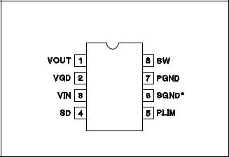
CONNECTION DIAGRAM
DIL-8, SOIC-8 (Top View)
N or J Package, D Package
Pin 6 is FB for UCC3941-ADJ.
ELECTRICAL CHARACTERISTICS: Unless otherwise specified, for UCC3941, TA = 0°C to 70°C; for UCC2941, TA = –40°C to 85°C; VIN = 1.25V, TA = TJ.
PARAMETER |
|
TEST CONDITIONS |
MIN |
TYP |
MAX |
UNITS |
VIN Section |
|
|
|
|
|
|
Minimum Startup Voltage |
No External VGD Load, TJ = 25°C, IOUT = 100mA (Note 1) |
|
0.8 |
1.0 |
V |
|
Minimum Start Voltage |
No External VGD Load, IOUT = 100mA, TJ = 0° C to 85° C |
|
0.9 |
1.1 |
V |
|
|
(Note 1) |
|
|
|
|
|
Minimum Startup Voltage |
No External VGD Load, TJ = –40°C to 0° C |
|
0.9 |
1.5 |
V |
|
Minimum Dropout Voltage |
No External VGD Load, IOUT = 100mA, VGD = 6.3V |
|
|
0.5 |
V |
|
|
(Note 1) |
|
|
|
|
|
Input Voltage Range |
|
|
1 |
|
VOUT |
V |
|
|
|
|
|
+0.5 |
|
Quiescent Supply Current |
(Note 2) |
|
13 |
25 |
µ A |
|
Supply Current at Shutdown |
SD = Open |
|
8 |
20 |
µ A |
|
Output Section |
|
|
|
|
|
|
Quiescent Supply Current |
(Note 2) |
|
32 |
80 |
µ A |
|
Supply Current at Shutdown |
SD = Open |
|
6 |
15 |
µ A |
|
Regulation Voltage (UCC3941-3) |
1V |
< VIN < 3V |
3.18 |
3.25 |
3.37 |
V |
|
1V |
< VIN < 3V, 0mA < IOUT < 150mA (Note 1) |
3.17 |
3.30 |
3.43 |
V |
Regulation Voltage (UCC3941-5) |
1V |
< VIN < 5V |
4.85 |
5.00 |
5.15 |
V |
|
1V |
< VIN < 5V, 0mA < IOUT 100mA (Note 1) |
4.8 |
5.0 |
5.2 |
V |
FB Voltage (UCC3941-ADJ) |
1V |
< VIN < 3V |
1.212 |
1.250 |
1.288 |
V |
VGD Output Section |
|
|
|
|
|
|
Quiescent Supply Current |
(Note 2) |
|
25 |
60 |
µ A |
|
Supply Current at Shutdown |
SD = Open |
|
8 |
20 |
µ A |
|
Regulation Voltage |
1V |
< VIN < 3V |
7.5 |
8.7 |
9.2 |
V |
|
1V |
< VIN < 3V, 0mA < IOUT < 10mA (Note 1) |
7.4 |
8.7 |
9.3 |
V |
Inductor Charging Section (L = 22µ H) |
|
|
|
|
|
|
Peak Discontinuous Current |
Over Operating Range |
|
0.50 |
0.85 |
A |
|
Peak Continuous Current |
RPLIM = 6.2Ω , UCC3941-3 and UCC3941-5 |
0.5 |
0.8 |
1.1 |
A |
|
|
UCC3941-ADJ |
0.6 |
0.9 |
1.3 |
A |
|
2

UCC2941-3/-5/-ADJ
UCC3941-3/-5/-ADJ
ELECTRICAL CHARACTERISTICS: Unless otherwise specified, for UCC3941, TA = 0°C to 70°C; for UCC2941, TA = –40°C to 85°C; VIN = 1.25V, TA = TJ.
PARAMETER |
TEST CONDITIONS |
MIN |
TYP |
MAX |
UNITS |
Inductor Charging Section |
|
|
|
|
|
Charge Switch RDS(on) |
N and D Package, I = 200mA |
|
0.25 |
0.4 |
Ω |
Current Limit Delay |
(Note 1) |
|
50 |
|
ns |
Synchronous Rectifier Section |
|
|
|
|
|
Rectifier RDS(on) |
N and D Package, I = 200mA, UCC3941-ADJ VOUT = 3.3V |
|
0.35 |
0.6 |
Ω |
|
and UCC3941–3 |
|
|
|
|
|
N and D Package, I = 200mA, UCC3941-5 |
|
0.5 |
0.8 |
Ω |
Shutdown Section |
|
|
|
|
|
Shutdown Bias Current |
|
–10 |
–7 |
|
µ A |
Note 1: Performance from application circuit shown in Figures 3 - 5 guaranteed by design and alternate testing methods, but not 100% tested as shown in production.
Note 2: For the UCC3941-3, VOUT = 3.47V and VGD = 9.3V. For the UCC3941-5, VOUT = 5.25V, VGD = 9.3V. For the UCC3941ADJ, FB = 1.315V, VGD = 9.3V.
PIN DESCRIPTIONS
FB: Feedback control pin used in the UCC3941-ADJ version only. The internal reference for this comparator is 1.25V and external resistors provide the gain to the output voltage.
PGND: Power ground of the IC. The inductor charging current flows through this pin. For the UCC3941-ADJ signal ground and power ground lines are tied to a common pin.
PLIM: This pin is programmed to set the maximum input power for the converter. For example a 1A current limit at 1V would have a 333mA limit at 3V input keeping the input power constant at 1W. The peak current at VIN = 1V is programmed to 1.5A (1.5W) when this pin is grounded. The power limit is given by:
11.8 • n
PL(W) = RPL + 6.7 + VIN (0 .26)
where RPL is equal to the external resistor from the PLIM pin to ground and n is the expected efficiency of the converter. The peak current limit is given by:
IPK (A) |
= |
|
11.8 • |
n |
|
+ 0 .26 |
||
|
|
|
|
|
||||
VIN • |
(RPL + |
6.7) |
||||||
|
|
|
||||||
Constant power gives several advantages over constant current such as lower output ripple.
SD: When this pin is open, the built in 7 A current source pulls up on the pin and programs the IC to go into shutdown mode. This pin requires an open circuit for shutdown and will not operate correctly when driven to a logic level high with TTL or CMOS logic. When this pin is connected to ground, (either directly or with a transistor) the IC is enabled and both output voltages will regulate.
SGND: Signal ground of the IC. For the UCC3941-ADJ signal ground and power ground lines are tied to a common pin.
SW: An inductor is connected between this node and VIN. The VGD (Gate Drive Supply) flyback diode is also connected to this pin. When servicing the 3.3V supply, this pin will go low charging the inductor, then shut off, dumping the energy through the synchronous rectifier to the output. When servicing the VGD supply, the internal synchronous rectifier stays off, and the energy is diverted to VGD through the flyback diode. During discontinuous portions of the inductor current a MOSFET resistively connects VIN to SW damping excess circulating energy to eliminate undesired high frequency ringing.
VGD: The VGD pin which is coarsely regulated around 9V and is primarily used for the gate drive supply for the power switches in the IC. This pin can be loaded with up to 10mA as long as it does not present a load at voltages below 2V. This ensures proper startup of the IC. The VGD supply can go as low as 7.5V without interfering with the servicing of the 3.3V output. Below 7.5V, VGD will have the highest priority, although practically the voltage should not decay to that level if the output capacitor is sized properly.
VIN: Input voltage to supply the IC during startup. After the output is running the IC draws power from VOUT or VGD.
VOUT: Main output voltage (3.3V, 5V or adjustable) which has highest priority in the multiplexing scheme, as long as VGD is above the critical level of 7.5V. Loads over 150mA are achievable at 1V input voltage. This output will startup with 1V input at full load.
3

APPLICATION INFORMATION
A detailed block diagram of the UCC3941 is shown in Fig. 1. Unique control circuitry provides high efficiency power conversion for both light and heavy loads by transitioning between discontinuous and continuous conduction based on load conditions. Fig. 2 depicts converter
UCC2941-3/-5/-ADJ
UCC3941-3/-5/-ADJ
waveforms for the application circuit shown in Fig. 3. A single 22 H inductor provides the energy pulses required for a highly efficient 3.3V converter at up to 500mW output power.
VIN |
SW |
|
|
|
|
3 |
|
|
|
8 |
|
|
|
|
|
|
|
|
|
|
ANTI-RINGING |
|
|
|
|
|
|
|
|
|
|
|
|
|
|
|
SWITCH |
|
|
|
|
|
|
|
|
|
|
VGD |
|
200kHz |
|
|
|
|
VGD ZERO |
VOUT ZERO |
|
|
|
|
|
|
|
STARTUP |
|
|
|
|
DETECT |
DETECT |
|
|
|
|
||
VGD |
2 |
|
|
|
|
|
|
|
|
|
||||
|
OSCILATOR |
|
|
|
VGD |
+ |
– |
|
|
|
|
|||
|
|
|
AND CONTROL |
|
|
|
|
|
|
|
||||
|
|
|
|
|
|
|
– |
+ |
|
|
|
|
||
|
|
|
|
|
|
|
|
|
|
|
|
|
||
|
|
+ |
|
|
|
|
|
|
|
|
1.7µ S |
|
|
|
|
|
|
|
|
|
|
|
|
OFF TIME |
|
|
|
||
|
|
|
|
|
|
|
|
|
|
|
|
|
||
|
5V |
– |
|
|
|
|
|
|
|
CONTROLLER |
|
|
|
|
|
|
|
|
|
|
|
|
|
|
|
|
VGD |
|
|
|
|
|
|
|
FROM |
|
|
|
|
|
|
|
|
|
|
|
|
|
|
SD |
|
|
|
|
|
|
|
RECTIFIER |
|
|
|
|
|
|
|
|
|
|
|
|
|
|
|
|
|
|
|
|
|
|
|
|
|
|
|
|
|
CONTROL |
|
|
|
|
1.4A |
|
|
|
|
|
|
|
|
|
FROM SD |
|
|
5Ω |
|
|
|
|
|
|
|
|
|
|
|
|
|
|
|
MAX |
|
|
|
|
|
|
|
|
|
|
|
|
PLIM |
5 |
|
|
|
|
|
|
|
|
|
|
|
|
|
|
|
|
CURRENT |
|
|
|
|
|
|
|
CLK |
|
|
|
|
|
|
|
|
|
|
|
|
|
D |
Q |
|
||
|
|
|
|
LIMIT |
|
|
|
|
|
|
|
|
||
|
|
|
|
+ |
|
|
|
|
|
|
|
L1 |
|
|
|
|
|
|
|
|
|
|
|
|
|
|
|
|
|
|
50mV |
|
– |
|
|
|
|
|
|
|
|
|
|
|
|
MAXIMUM |
|
|
|
|
|
|
|
|
|
|
|||
|
|
|
|
|
|
|
|
|
|
|
|
|||
|
|
|
|
|
VSAT |
|
|
|
|
|
R |
Q |
|
|
|
SD |
|
|
VIN |
|
|
|
|
|
|
|
|
|
|
|
|
50mV |
|
ON TIME |
|
|
SD |
|
|
|
||||
SD |
4 |
|
|
CONTROLLER |
|
|
|
|
|
|||||
|
VIN |
|
|
|
BOOST |
|
|
|||||||
|
|
|
|
|
|
|
11µ SEC |
|
|
|
|
|||
|
|
|
|
|
T |
|
= |
|
|
|
|
|||
|
|
|
|
|
|
|
|
LATCH |
|
|
||||
|
|
|
|
|
|
ON |
|
VIN |
|
|
|
|
||
|
|
|
|
|
|
|
|
|
|
|
|
|
– |
|
|
|
|
|
|
|
|
|
|
|
|
|
|
+ |
* |
|
|
|
|
|
|
|
|
Q |
R |
|
|
|
– |
VGD |
|
|
|
|
|
|
|
|
|
SD |
|
|
|
||
|
|
|
|
|
|
|
|
|
|
|
|
+ |
** |
|
|
|
|
|
|
|
|
|
|
|
|
|
|
||
|
|
|
|
THERMAL |
|
|
|
|
|
|
|
|
|
|
|
|
|
|
SHUTDOWN |
|
|
|
|
|
|
|
|
|
VGD |
|
|
|
|
|
|
|
|
|
|
|
|
|
– |
|
|
|
|
|
|
|
|
|
|
|
|
|
|
+ |
*** |
|
|
|
|
|
* 3.3V FOR UCC3941-3 |
** 8.7V FOR UCC3941-3 |
*** 7.7V FOR UCC3941-3 |
|
|
|||||
|
|
|
|
|
5.0V FOR UCC3941-5 |
|
|
|||||||
|
|
|
|
|
9.6V FOR UCC3941-5/-ADJ |
8.8V FOR UCC3941-5/-ADJ |
|
|
||||||
|
|
|
|
|
1.25V FOR UCC3941-ADJ |
|
|
|||||||
|
|
|
|
|
|
|
|
|
|
|
||||
1 VOUT
FB FOR
6UCC3941-ADJ ONLY
6SGND FOR UCC3941-3/-5
7PGND
Note: Switches are shown in the logic low state. |
UDG-98146 |
Figure 1. 1V Synchronous boost.
4
 Loading...