


 Loading...
Analog Devices DAC8426AR, DAC8426FS, DAC8426FR, DAC8426FP, DAC8426ER Datasheet
...a Quad 8-Bit Voltage Out CMOS DAC
Complete with Internal 10 V Reference
DAC8426
FEATURES
No Adjustments Required, Total Error 61 LSB Max
Over Temperature
Four Voltage-Output DACs on a Single Chip Internal 10 V Bandgap Reference
Operates from Single 115 V Supply
Fast 50 ns Data Load Time, All Temperatures Pin-for-Pin Replacement for PM-7226 and AD7226,
Eliminates External Reference
APPLICATIONS
Process Controls
Multichannel Microprocessor Controlled:
System Calibration
Op Amp Offset and Gain Adjust
Level and Threshold Setting
offering a 25 ppm/°C temperature coefficient and 5 mA of external load driving capability.
The DAC8426 contains four 8-bit voltage-output CMOS D/A converters on a single chip. A 10 V output bandgap reference sets the output full-scale voltage. The circuit also includes four input latches and interface control logic.
One of the four latches, selected by the address inputs, is loaded from the 8-bit data bus input when the write strobe is active low. All digital inputs are TTL/CMOS (5 V) compatible. The on-board amplifiers can drive up to 10 mA from either a single or dual supply. The on-board reference that is always connected to the internal DACs has 5 mA available to drive external devices.
Its compact size, low power, and economical cost-per-channel, make the DAC8426 attractive for applications requiring multiple D/A converters without sacrificing circuit-board space. System reliability is also increased due to reduced parts count.
GENERAL DESCRIPTION
The DAC8426 is a complete quad voltage output D/A converter with internal reference. This product fits directly into any existing 7226 socket where the user currently has a 10 V external reference. The external reference is no longer necessary. The internal reference of the DAC8426 is laser-trimmed to ±0.4%
PMI’s advanced oxide-based, silicon-gate, CMOS process allows the DAC8426’s analog and digital circuitry to be manufactured on the same chip. This, coupled with PMI’s highly stable thin-film R-2R resistor ladder, aids in matching and temperature tracking between DACs.
FUNCTIONAL BLOCK DIAGRAM
REV. C
Information furnished by Analog Devices is believed to be accurate and reliable. However, no responsibility is assumed by Analog Devices for its use, nor for any infringements of patents or other rights of third parties which may result from its use. No license is granted by implication or otherwise under any patent or patent rights of Analog Devices.
One Technology Way, P.O. Box 9106, Norwood, MA 02062-9106, U.S.A. Tel: 617/329-4700 Fax: 617/326-8703
DAC8426–SPECIFICATIONS (VDD = +15 V 6 10%, AGND = DGND = 0 V, VSS = 0 V, TA = –558C to +1258C applies for DAC8426AR/BR, TA = –408C to +858C applies for DAC8426ER/EP/FR/FP/FS, unless otherwise noted.)
Parameter |
Symbol |
Conditions |
|
Min |
Typ |
Max |
Units |
|
|
|
|
|
|
|
|
STATIC PERFORMANCE |
|
|
|
|
|
|
|
Resolution |
N |
|
|
8 |
|
±1 |
Bits |
Total Unadjusted Error1 |
TUE |
Includes Reference |
A, E |
|
|
LSB |
|
|
|
|
B, F |
|
|
±2 |
LSB |
Relative Accuracy |
INL |
|
A, E |
|
|
±1/2 |
LSB |
|
|
|
B, F |
|
|
± 1 |
LSB |
Differential Nonlinearity2 |
DNL |
|
|
|
|
±1 |
LSB |
Full-Scale Temperature Coefficient |
TCGFS |
Includes Reference |
|
|
25 |
|
ppm/°C |
Zero Scale Error |
VZSE |
|
|
|
|
20 |
mV |
Zero Scale Error |
|
|
|
|
|
|
μV/°C |
Temperature Coefficient |
TCVZS |
Dual Supply |
VSS = –5 V |
|
10 |
|
|
REFERENCE OUTPUT |
|
|
|
|
|
|
|
Output Voltage |
VREFOUT |
No Load |
A, E |
9.96 |
|
10.04 |
V |
|
|
|
B, F |
9.92 |
|
10.08 |
V |
Temperature Coefficient |
TCVREFOUT |
|
|
|
20 |
|
ppm/°C |
Load Regulation |
LDREG |
IL = 5 mA |
|
|
0.02 |
0.1 |
%/mA |
Line Regulation |
LNREG |
VDD ±10% |
|
|
0.008 |
0.04 |
%/V |
Output Noise3 |
en rms |
f = 0.1 Hz to 10 Hz |
|
|
3 |
10 |
μV p-p |
Output Current |
IREFOUT |
VREFOUT < 40 mV |
|
5 |
7 |
|
mA |
DIGITAL INPUTS |
|
|
|
|
|
|
|
Logic Input “0” |
VINL |
|
|
|
|
0.8 |
V |
Logic Input “1” |
VINH |
|
|
2.4 |
|
|
V |
Input Current |
IIN |
VIN = 0 V or VDD |
|
|
0.1 |
10 |
μA |
Input Capacitance3 |
CIN |
|
|
|
4 |
8 |
pF |
POWER SUPPLIES |
|
|
|
|
|
|
|
Positive Supply Current4 |
IDD |
|
|
|
6 |
14 |
mA |
Negative Supply Current4 |
ISS |
Dual Supply |
VSS = –5 V |
|
4 |
10 |
mA |
Power Dissipation5 |
PDISS |
VDD = ±5% |
|
|
90 |
210 |
mW |
Power Supply Sensitivity |
PSS |
|
|
0.0002 |
0.01 |
%/% |
VDD = +15 V 6 10%, AGND = DGND = 0 V, VSS = 0 V, TA = –558C to +1258C applies for DAC8426AR/BR, TA = –408C to +858C applies for DAC8426ER/EP/FR/FP/FS, unless otherwise noted.
Parameter |
Symbol |
Conditions |
Min |
Typ6 Max |
Units |
|
|
|
|
|
|
DAC OUTPUT |
|
|
|
|
|
Output Current (Source)3 |
IOUTSOURCE |
Digital In = All Ones |
10 |
|
mA |
Output Current (Sink)3 |
IOUTSINK |
Digital In = All Zeroes VSS = –5 V |
350 |
450 |
μA |
Minimum Load Resistance |
RL(MIN) |
Digital In = All Ones |
2 |
|
kΩ |
DYNAMIC PERFORMANCE3 |
|
|
|
|
V/μs |
VOUT Slew Rate |
SR |
To ± 1/2 LSB, RL = 2 kΩ |
|
4 |
|
VOUT Settling Time |
tS |
|
3 |
μs |
|
(Positive or Negative) |
|
|
|
|
|
Digital Crosstalk |
Q |
|
|
10 |
nVs |
|
|
|
|
|
|
SWITCHING CHARACTERISTICS3 |
|
|
|
|
|
Address To Write Setup Time |
tAS |
|
0 |
|
ns |
Address To Write Hold Time |
tAH |
|
0 |
|
ns |
Data Valid To Write Setup Time |
tDS |
|
70 |
|
ns |
Data Valid To Write Hold Time |
tDH |
|
10 |
|
ns |
Write Pulse Width |
tWR |
|
50 |
|
ns |
NOTES
1Includes Full-Scale Error, Relative Accuracy, and Zero Code Error. Note ± 1 LSB = ± 0.39% error. 2All devices guaranteed monotonic over the full operating temperature range.
3Guaranteed and not subject to production test.
4Digital inputs VIN = VINL or VINH; VOUT and VREFOUT unloaded. 5PDISS calculated by IDD × VDD.
6Typicals represent measured characteristics at TA = +25°C. Specifications subject to change without notice.
–2– |
REV. C |
DAC8426
ABSOLUTE MAXIMUM RATINGS |
|
VDD to AGND or DGND . . . . . . . . . . . . . . |
. . . –0.3 V, +17 V |
VSS to AGND or DGND . . . . . . . . . . . . . . . |
. . . . . . –7 V, VDD |
VDD to VSS . . . . . . . . . . . . . . . . . . . . . . . . . . |
. . –0.3 V, +24 V |
AGND to DGND . . . . . . . . . . . . . . . . . . . . . |
. . . –0.3 V, +5 V |
Digital Input Voltage to DGND . . . . . . . . . . |
. . . –0.3 V, VDD |
VREFOUT to AGND1 . . . . . . . . . . . . . . . . . . |
. . . –0.3 V, VDD |
VOUT to AGND1 . . . . . . . . . . . . . . . . . . . . . . |
. . . . . . VSS, VDD |
Operating Temperature |
–55°C to +125°C |
Military AR/BR . . . . . . . . . . . . . . . . . . . . |
Extended Industrial ER/EP/FR/FP/FS |
. . . . –40°C to +85°C |
Maximum Junction Temperature . . . . . . |
. . . . . . . . . . +150°C |
Storage Temperature . . . . . . . . . . . . . . . |
. . . –65°C to +150°C |
Lead Temperature (Soldering, 60 sec) . . |
. . . . . . . . . . +300°C |
THERMAL RESISTANCE
Package Type |
uJA2 |
uJC |
Units |
20-Pin Cerdip (R) |
70 |
7 |
°C/W |
20-Pin Plastic DIP (P) |
61 |
24 |
°C/W |
20-Pin SOL(S) |
80 |
22 |
°C/W |
NOTES
1Outputs may be shorted to any terminal provided the package power dissipation is not exceeded. Typical output short-circuit current to AGND is 50 mA.
2θJA is specified for worst case mounting conditions, i.e., θJA is specified for device in socket for cerdip and P-DIP packages; θJA is specified for device soldered to printed circuit board for SOL package.
CAUTION
1.Do not apply voltages higher than VDD or less than VSS potential on any terminal.
2.The digital control inputs are zener-protected; however, permanent damage may occur on unprotected units from high-energy electrostatic fields. Keep units in conductive foam at all times until ready to use.
3.Do not insert this device into powered sockets. Remove power before insertion or removal.
4.Stresses above those listed under “Absolute Maximum Ratings” may cause permanent damage to device.
PIN CONNECTIONS
20-Pin Cerdip
(R Suffix)
20-Pin Epoxy DIP
(P Suffix)
20-Pin SOL
(S Suffix)
ORDERING GUIDE1
Model |
Total Unadjusted Error |
Temperature Range |
Package Description |
|
|
|
|
DAC8426AR2 |
±1 LSB |
–55°C to +125°C |
20-Pin Cerdip (Q-20) |
DAC8426ER |
±1 LSB |
–40°C to +85°C |
20-Pin Cerdip (Q-20) |
DAC8426EP |
±1 LSB |
–40°C to +85°C |
20-Pin Plastic DIP (N-20) |
DAC8426BR2 |
±2 LSB |
–55°C to +125°C |
20-Pin Cerdip (Q-20) |
DAC8426FR |
±2 LSB |
–40°C to +85°C |
20-Pin Cerdip (Q-20) |
DAC8426FP |
±2 LSB |
–40°C to +85°C |
20-Pin Plastic DIP (N-20) |
DAC8426FS3 |
±2 LSB |
–40°C to +85°C |
20-Lead SOL (R-20) |
NOTES
1Burn-in is available on commercial and industrial temperature range parts in cerdip, plastic DIP, and TO-can packages. 2For devices processed in total compliance to MIL-STD-883, add /883 after part number. Consult factory for 883 data sheet. 3For availability and burn-in information on SO and PLCC packages, contact your local sales office.
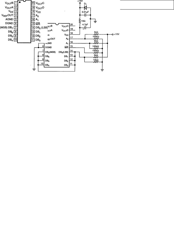
Burn-In Circuit
REV. C |
–3– |

DAC8426
DICE CHARACTERISTICS
1. |
VOUT B |
11. |
DB3 |
2. |
VOUT A |
12. |
DB2 |
3. |
VSS |
13. |
DB1 |
4. VREF OUT |
14. DB0 (LSB) |
||
5. AGND |
15. WR |
||
6. DGND |
16. A1 |
||
7. |
DB7 (MSB) |
17. |
A0 |
8. |
DB6 |
18. |
VDD |
9. |
DB5 |
19. |
VOUT D |
10. DB4 |
20. |
VOUT C |
|
DIE SIZE 0.129 × 0.152 inch, 19,608 sq. mils (3.28 × 3.86 mm, 12.65 sq. mm)
WAFER TEST LIMITS at VDD = +15 V 6 5%; VSS = AGND = DGND = 0 V; unless otherwise specified. TA = +258C. All specifications apply for DACs A, B, C, and D.
|
|
|
DAC8426GBC |
|
Parameter |
Symbol |
Conditions |
Limits |
Units |
|
|
|
|
|
Total Unadjusted Error |
TUE |
|
±2 |
LSB max |
Relative Accuracy |
INL |
|
±1 |
LSB max |
Differential Nonlinearity |
DNL |
|
±1 |
LSB max |
Full-Scale Error |
GFSE |
|
±1 |
LSB max |
Zero Code Error |
VZSE |
|
±20 |
mV max |
DAC Output Current |
IOUTSOURCE |
Digital In = All Ones |
10 |
mA min |
Reference Output Voltage |
VREFOUT |
No Load |
10.04 |
V max |
Load Regulation |
LDREG |
IL = 5 mA |
0.1 |
%/mA max |
Line Regulation |
LNREG |
VDD = ±10 V |
0.04 |
%/V max |
Reference Output Current |
IREFOUT |
VREFOUT < 40 mV |
5 |
mA min |
Logic Inputs High |
VINH |
|
2.4 |
V min |
Logic Inputs Low |
VINL |
|
0.8 |
V max |
Logic Input Current |
IIN |
VIN = 0 V or VDD |
±1 |
μA max |
Positive Supply Current |
IDD |
VIN = VINL or VINH |
14 |
mA max |
Negative Supply Current |
ISS |
VIN = VINL or VINH’ VSS = –5 V |
10 |
mA max |
NOTE
Electrical tests are performed at wafer probe to the limits shown. Due to variations in assembly methods and normal yield loss, yield after packaging is not guaranteed for standard product dice. Consult factory to negotiate specifications based on dice lot qualifications through sample lot assembly and testing.
CAUTION
ESD (electrostatic discharge) sensitive device. Electrostatic charges as high as 4000 V readily accumulate on the human body and test equipment and can discharge without detection. Although the DAC8426 features proprietary ESD protection circuitry, permanent damage may occur on devices subjected to high energy electrostatic discharges. Therefore, proper ESD precautions are recommended to avoid performance degradation or loss of functionality.
WARNING!
ESD SENSITIVE DEVICE
–4– |
REV. C |
Loading...