


Texas Instruments UCC3958PWPTR-4, UCC3958PWPTR-3, UCC3958PWPTR-2, UCC3958PWPTR-1, UCC3958PWP-4 Datasheet
...
UCC3958 -1/-2/-3/-4
Single Cell Lithium-Ion Battery Protection Circuit
PRELIMINARY
FEATURES
∙Protects Sensitive Lithium-Ion Cells Form Over Charging and Over Discharging
∙Dedicated for One Cell Applications
∙Does Not Require External FETs or Sense Resistors
∙Internal Precision Trimmed Charge and Discharge Voltage Limits
∙Extremely Low Power Drain
∙Low FET Switch Voltage Drop of 150mV Typical for 3A Currents
∙Short Circuit Current Protection (with User Programmable Delay)
∙3A Current Capacity
∙Thermal Shutdown
∙User Controlled Enable Pin
DESCRIPTION
UCC3958 is a monolithic BCMOS lithium-ion battery protection circuit that is designed to enhance the useful operating life of one cell rechargeable battery packs. Cell protection features consist of internally trimmed charge and discharge voltage limits, discharge current limit with a delayed shutdown and an ultra low current sleep mode state when the cell is discharged. Additional features include an on chip MOSFET for reduced external component count and a charge pump for reduced power losses while charging or discharging a low cell voltage battery pack. This protection circuit requires a minimum number of external components and is able to operate and safely shutdown in the presence of a short circuit load.
BLOCK DIAGRAM
UDG-98050 |
6/98 |
UCC3958 -1/-2/-3/-4
ABSOLUTE MAXIMUM RATINGS
Supply Voltage (PACK+ to BNEG) . . . . . . . . . . . . . . . . . . . 7.5V
Maximum Continuous Charge Current . . . . . . . . . . . . . . . . . 3A
Maximum Charger Voltage (PACK+ to PACK–) . . . . . . . . . . 9V
Maximum Reverse Voltage (PACK+ to PACK–) . . . . . . . . . –8V
Storage Temperature . . . . . . . . . . . . . . . . . . . –65°C to +150°C
Junction Temperature. . . . . . . . . . . . . . . . . . . –55°C to +150°C
Lead Temperature (Soldering, 10 sec.) . . . . . . . . . . . . . +300°C
Currents are positive into, negative out of the specified terminal. Consult Packaging Section of Databook for thermal limitations and considerations of packages.
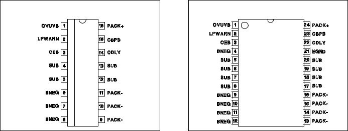
CONNECTION DIAGRAMS
SOIC-16 (Top View)
DP Package
TSSOP-24 (Top View)
PWP Package
ELECTRICAL CHARACTERISTICS: Unless otherwise specified, PACK+ = 4V, –20°C < T A < 70°C. All voltages measured with respect to BNEG. TA = TJ.
PARAMETER |
TEST CONDITIONS |
MIN |
TYP |
MAX |
UNITS |
State Transition Thresholds |
|
|
|
|
|
NORM to OV (VOV) |
UCC3958-1 |
4.15 |
4.20 |
4.25 |
V |
OV to NORM (VTHI) |
UCC3958-1 |
3.85 |
3.90 |
3.95 |
V |
NORM to OV (VOV) |
UCC3958-2 |
4.20 |
4.25 |
4.30 |
V |
OV to NORM (VTHI) |
UCC3958-2 |
3.90 |
3.95 |
4.00 |
V |
NORM to OV (VOV) |
UCC3958-3 |
4.25 |
4.30 |
4.35 |
V |
OV to NORM (VTHI) |
UCC3958-3 |
3.95 |
4.00 |
4.05 |
V |
NORM to OV (VOV) |
UCC3958-4 |
4.30 |
4.35 |
4.40 |
V |
OV to NORM (VTHI) |
UCC3958-4 |
4.00 |
4.05 |
4.10 |
V |
NORM to UV (VUV) |
(Note 1) |
2.25 |
2.35 |
2.45 |
V |
UV to NORM (VTLO) |
|
2.55 |
2.65 |
2.75 |
V |
OV, UV Delay Time (TD) |
All Dash Numbers |
7 |
18 |
34 |
msec |
2
UCC3958 -1/-2/-3/-4
ELECTRICAL CHARACTERISTICS: Unless otherwise specified, PACK+ = 4V, –20°C < T A < 70°C. All voltages measured with respect to BNEG. TA = TJ.
PARAMETER |
TEST CONDITIONS |
MIN |
TYP |
MAX |
UNITS |
BNEG/PACK - SWITCH |
|
|
|
|
|
VBNEG - VPACK |
NORM, ISWITCH = 2A |
|
–100 |
–150 |
mV |
|
NORM, ISWITCH = –2A |
|
100 |
150 |
mV |
|
VPACK+ > VOV, ISWITCH = 20mA to 2A, |
|
–100 |
–300 |
mV |
|
(OV State) |
|
|
|
|
|
VPACK+ = 2.5V, ISWITCH = –20mA to –2A, |
|
100 |
600 |
mV |
|
(UV State) |
|
|
|
|
RDSON |
NORM ISWITCH = 2A |
|
50 |
75 |
mW |
|
NORM ISWITCH = –2A |
|
50 |
75 |
mW |
IBNEG – (Charger Leakage Current in OV) |
VPACK+ > VOV (OV State) |
|
1 |
20 |
mA |
|
([VPACK+] – [VPACK–]=6V) |
|
|
|
|
BIAS Current |
|
|
|
|
|
IPACK+ |
VPACK+ > VUV |
|
7 |
20 |
mA |
IPACK+ |
In Super Low Power Mode (VPACK+ < VUV) |
|
1 |
1.5 |
mA |
VBAT |
Minimum Operating Cell Voltage |
|
|
1.5 |
V |
Battery Sample Rate (TS) |
|
7 |
12 |
17 |
ms |
Short Circuit Protection |
|
|
|
|
|
ITHLD |
|
2.75 |
5.25 |
7.25 |
A |
TDLY |
CDLY = 0 |
|
350 |
|
ms |
|
CDLY = 100pF |
|
2.5 |
|
ms |
|
(Maximum Recommended Value) |
|
|
|
|
RRESET |
Overcurrent Reset Resistance |
7.5 |
|
|
MΩ |
LPWARN Output |
|
|
|
|
|
LP Warn Threshold |
|
2.55 |
2.65 |
2.75 |
V |
TR |
CLOAD = 100pF, 10% to 90% of PACK+ |
|
280 |
560 |
ns |
TF |
CLOAD = 100pF, 10% to 90% of PACK+ |
|
120 |
280 |
ns |
VHIGH (VPACK+ –VLPWARN) |
ISINK = 200mA, VUV < VPACK+ < VTLO |
|
0.3 |
0.4 |
V |
VLOW |
ISOURCE = 200mA, VTLO < VPACK+ < VUV |
|
0.3 |
0.4 |
V |
Measure Delay |
|
|
6 |
|
ms |
OVUVB Output |
|
|
|
|
|
TR |
CLOAD = 100pF, Hi Z to 90% of PACK+ |
|
280 |
560 |
ns |
TF |
CLOAD = 100pF, Hi Z to 10% of PACK+ |
|
140 |
280 |
ns |
VHIGH (VPACK+ – VOVUVB) |
ISOURCE = 200mA, VPACK+ ³ VOV |
|
0.3 |
0.4 |
V |
VLOW |
ISINK = 200mA, VPACK+ ≤ VUV |
|
0.3 |
0.4 |
V |
ZOUT |
Output Tristated |
|
10 |
|
MW |
Measure Delay |
|
|
18 |
|
ms |
CE Input |
|
|
|
|
|
ISINK |
|
|
150 |
|
nA |
Note 1: Other threshold voltages are available.
3
 Loading...