


TEXAS INSTRUMENTS TIBPAL16L8-5C, TIBPAL16R4-5C, TIBPAL16R6-5C, TIBPAL16R8-5C, TIBPAL16L8-7M Technical data
...5962-8515521RA TIBPAL16L8-5C, TIBPAL16R4-5C, TIBPAL16R6-5C, TIBPAL16R8-5C
TIBPAL16L8-7M, TIBPAL16R4-7M, TIBPAL16R6-7M, TIBPAL16R8-7M HIGH-PERFORMANCE IMPACT-X PAL CIRCUITS
|
SRPS011D ± D3359, OCTOBER 1989 ± REVISED SEPTEMBER 1992 |
||||||
|
|
|
|
|
|
||
• High-Performance Operation: |
|
TIBPAL16L8' |
|
||||
C SUFFIX . . . J OR N PACKAGE |
|||||||
fmax (no feedback) |
|||||||
M SUFFIX . . . J PACKAGE |
|||||||
TIBPAL16R ' -5C Series . . . 125 MHz Min |
|
(TOP VIEW) |
|
||||
TIBPAL16R ' -7M Series . . . 100 MHz Min |
|
|
|||||
|
|
|
|
|
|
||
fmax (internal feedback) |
I |
|
1 |
20 |
|
VCC |
|
|
|
||||||
TIBPAL16R ' -5C Series . . . 125 MHz Min |
|
|
|||||
|
|
||||||
TIBPAL16R ' -7M Series . . . 100 MHz Min |
I |
|
2 |
19 |
|
O |
|
I |
|
3 |
18 |
|
I/O |
||
|
|
||||||
fmax (external feedback) |
|
|
|||||
I |
|
4 |
17 |
|
I/O |
||
|
|
||||||
TIBPAL16R ' -5C Series . . . 117 MHz Min |
|
|
|||||
I |
|
5 |
16 |
|
I/O |
||
TIBPAL16R ' -7M Series . . . 74 MHz Min |
|
|
|||||
I |
|
6 |
15 |
|
I/O |
||
Propagation Delay |
|
|
|||||
I |
|
7 |
14 |
|
I/O |
||
TIBPAL16L8-5C Series . . . 5 ns Max |
|
|
|||||
I |
|
8 |
13 |
|
I/O |
||
TIBPAL16L8-7M Series . . . 7 ns Max |
|
|
|||||
I |
|
9 |
12 |
|
O |
||
TIBPAL16R ' -5C Series |
|
|
|||||
GND |
|
|
|
||||
(CLK-to-Q) . . . 4 ns Max |
|
10 |
11 |
|
I |
||
|
|
|
|
|
|||
TIBPAL16R ' -7M Series
(CLK-to-Q) . . . 6.5 ns Max
•Functionally Equivalent, but Faster than, Existing 20-Pin PLDs
•Preload Capability on Output Registers Simplifies Testing
•Power-Up Clear on Registered Devices (All Register Outputs are Set Low, but Voltage Levels at the Output Pins Go High)
•Package Options Include Both Plastic and Ceramic Chip Carriers in Addition to Plastic and Ceramic DIPs
•Security Fuse Prevents Duplication
|
I |
3-STATE |
REGISTERED |
I/O |
|
DEVICE |
PORT |
||||
INPUTS |
O OUTPUTS |
Q OUTPUTS |
|||
|
S |
||||
|
|
|
|
||
|
|
|
|
|
|
'PAL16L8 |
10 |
2 |
0 |
6 |
|
|
|
|
|
|
|
'PAL16R4 |
8 |
0 |
4 (3-state buffers) |
4 |
|
|
|
|
|
|
|
'PAL16R6 |
8 |
0 |
6 (3-state buffers) |
2 |
|
|
|
|
|
|
|
'PAL16R8 |
8 |
0 |
8 (3-state buffers) |
0 |
TIBPAL16L8'
C SUFFIX . . . FN PACKAGE M SUFFIX . . . FK PACKAGE
(TOP VIEW)
|
|
|
|
CC |
O |
|
|
I I I V |
|
||||
I |
3 |
2 |
1 |
20 19 |
I/O |
|
4 |
|
|
|
18 |
||
I |
5 |
|
|
|
17 |
I/O |
I |
6 |
|
|
|
16 |
I/O |
I |
7 |
|
|
|
15 |
I/O |
I |
8 |
|
|
|
14 |
I/O |
|
9 |
10 11 12 13 |
|
|||
|
I |
GND |
I |
O |
I/O |
|
Pin assignments in operating mode
description
These programmable array logic devices feature high speed and functional equivalency when compared with currently available devices. These IMPACT-X circuits combine the latest Advanced Low-Power Schottky technology with proven titanium-tungsten fuses to provide reliable, high-performance substitutes for conventional TTL logic. Their easy programmability allows for quick design of custom functions and typically results in a more compact circuit board.
The TIBPAL16' C series is characterized from 0°C to 75°C. The TIBPAL16' M series is characterized for operation over the full military temperature range of ±55°C to 125°C.
These devices are covered by U.S. Patent 4,410,987.
IMPACT-X is a trademark of Texas Instruments Incorporated.
PAL is a registered trademark of Advanced Micro Devices Inc.
This document contains information on products in more than one phase |
Copyright 1992, Texas Instruments Incorporated |
of development. The status of each device is indicated on the page(s) |
|
specifying its electrical characteristics. |
|
POST OFFICE BOX 655303 •DALLAS, TEXAS 75265 |
1 |
TIBPAL16R4-5C, TIBPAL16R6-5C, TIBPAL16R8-5C
TIBPAL16R4-7M, TIBPAL16R6-7M, TIBPAL16R8-7M
HIGH-PERFORMANCE IMPACT-X PAL CIRCUITS
SRPS011D ± D3359, OCTOBER 1989 ± REVISED SEPTEMBER 1992
TIBPAL16R4' |
TIBPAL16R4' |
C SUFFIX . . . J OR N PACKAGE |
C SUFFIX . . . FN PACKAGE |
M SUFFIX . . . J PACKAGE |
M SUFFIX . . . FK PACKAGE |
(TOP VIEW) |
(TOP VIEW) |
|
CLK |
1 |
20 |
VCC |
|
|
|
CLK |
CC |
I/O |
|
|
I |
I |
V |
|
||||||
I |
2 |
19 |
I/O |
|
3 |
2 |
1 |
20 19 |
|
|
I |
3 |
18 |
I/O |
I |
I/O |
|||||
I |
4 |
17 |
Q |
4 |
|
|
|
18 |
||
I |
5 |
|
|
|
17 |
Q |
||||
I |
5 |
16 |
Q |
|
|
|
||||
I |
6 |
|
|
|
16 |
Q |
||||
I |
6 |
15 |
Q |
|
|
|
||||
I |
7 |
|
|
|
15 |
Q |
||||
I |
7 |
14 |
Q |
|
|
|
||||
I |
8 |
|
|
|
14 |
Q |
||||
I |
|
|
I/O |
|
|
|
||||
8 |
13 |
|
9 |
10 11 12 13 |
|
|||||
I |
9 |
12 |
I/O |
|
I |
GND |
OE |
I/O |
I/O |
|
GND |
10 |
11 |
OE |
|
|
|||||
|
|
|
|
|
|
|
||||
TIBPAL16R6' |
TIBPAL16R6' |
C SUFFIX . . . J OR N PACKAGE |
C SUFFIX . . . FN PACKAGE |
M SUFFIX . . . J PACKAGE |
M SUFFIX . . . FK PACKAGE |
(TOP VIEW)
(TOP VIEW)
CLK |
1 |
20 |
VCC |
|
|
|
CLK |
CC |
I/O |
|
|
|
I |
I |
V |
|
|||||||
I |
2 |
19 |
I/O |
|
3 |
2 |
1 |
20 19 |
|
||
I |
3 |
18 |
Q |
I |
Q |
||||||
4 |
|
|
|
18 |
|||||||
I |
4 |
17 |
Q |
I |
5 |
|
|
|
17 |
Q |
|
I |
5 |
16 |
Q |
I |
6 |
|
|
|
16 |
Q |
|
I |
6 |
15 |
Q |
I |
7 |
|
|
|
15 |
Q |
|
I |
7 |
14 |
Q |
I |
8 |
|
|
|
14 |
Q |
|
I |
8 |
13 |
Q |
|
9 |
10 11 12 13 |
|
||||
I |
9 |
12 |
I/O |
|
I |
GND |
OE |
I/O |
Q |
|
|
GND |
10 |
11 |
OE |
|
|
||||||
|
|
|
|
|
|
|
|||||
TIBPAL16R8' |
TIBPAL16R8' |
C SUFFIX . . . J OR N PACKAGE |
C SUFFIX . . . FN PACKAGE |
M SUFFIX . . . J PACKAGE |
M SUFFIX . . . FK PACKAGE |
(TOP VIEW) |
(TOP VIEW) |
|
CLK |
1 |
20 |
VCC |
|
|
|
CLK |
CC |
Q |
|
|
I |
I |
V |
|
||||||
I |
2 |
19 |
Q |
|
3 |
2 |
1 |
20 19 |
|
|
I |
3 |
18 |
Q |
I |
Q |
|||||
I |
4 |
17 |
Q |
4 |
|
|
|
18 |
||
I |
5 |
|
|
|
17 |
Q |
||||
I |
5 |
16 |
Q |
|
|
|
||||
I |
6 |
|
|
|
16 |
Q |
||||
I |
6 |
15 |
Q |
|
|
|
||||
I |
7 |
|
|
|
15 |
Q |
||||
I |
7 |
14 |
Q |
|
|
|
||||
I |
8 |
|
|
|
14 |
Q |
||||
I |
|
|
Q |
|
|
|
||||
8 |
13 |
|
9 |
10 11 12 13 |
|
|||||
I |
9 |
12 |
Q |
|
I |
GND |
OE Q |
Q |
|
|
GND |
10 |
11 |
OE |
|
|
|||||
|
|
|
|
|
|
|
||||
Pin assignments in operating mode
2 |
POST OFFICE BOX 655303 •DALLAS, TEXAS 75265 |
TIBPAL16L8-5C, TIBPAL16R4-5C
TIBPAL16L8-7M, TIBPAL16R4-7M HIGH-PERFORMANCE IMPACT-X PAL CIRCUITS
SRPS011D ± D3359, OCTOBER 1989 ± REVISED SEPTEMBER 1992
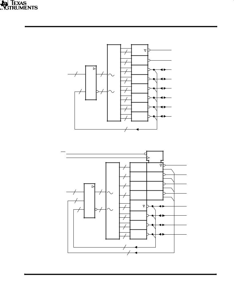
functional block diagrams (positive logic)
TIBPAL16L8'
|
& |
EN ≥ 1 |
|
|
32 X 64 |
7 |
|
|
|
7 |
|
|
16 x |
7 |
|
10 |
16 |
||
|
|||
I |
|
|
|
|
|
7 |
O
O
I/O
I/O
6 |
16 |
7 |
I/O |
|
|
7 |
I/O |
|
|
7 |
I/O |
|
|
7 |
I/O |
|
|
6 |
|
|
TIBPAL16R4' |
|
|
|
|
OE |
|
|
|
EN 2 |
|
CLK |
|
|
|
C1 |
|
|
& |
8 |
≥ 1 |
I = 0 2 |
Q |
|
32 X 64 |
|
|
1D |
|
|
|
|
|
|
|
|
|
8 |
|
|
Q |
|
16 x |
8 |
|
|
Q |
8 |
|
|
|
|
|
16 |
|
|
|
|
|
I |
|
8 |
|
|
Q |
|
|
|
|
||
4 |
|
|
|
|
|
|
|
7 |
EN ≥ 1 |
|
I/O |
4 |
16 |
|
|
||
|
|
7 |
|
|
I/O |
|
|
7 |
|
|
I/O |
|
|
7 |
|
|
I/O |
|
|
4 |
|
|
|
|
|
4 |
|
|
|
 denotes fused inputs
POST OFFICE BOX 655303 •DALLAS, TEXAS 75265 |
3 |
TIBPAL16R6-5C, TIBPAL16R8-5C
TIBPAL16R6-7M, TIBPAL16R8-7M HIGH-PERFORMANCE IMPACT-X PAL CIRCUITS
SRPS011D ± D3359, OCTOBER 1989 ± REVISED SEPTEMBER 1992
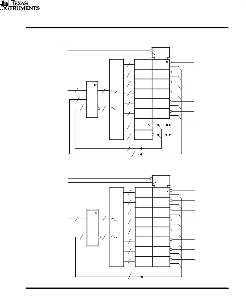
functional block diagrams (positive logic)
TIBPAL16R6'
OE |
|
|
|
EN 2 |
CLK |
|
|
|
C1 |
|
& |
8 |
≥ 1 |
I = 0 2 |
|
32 X 64 |
|
|
1D |
|
|
|
|
|
|
|
8 |
|
|
|
16 x |
8 |
|
|
8 |
|
|
|
|
16 |
|
|
|
|
I |
|
8 |
|
|
|
|
|
|
|
6 |
|
|
|
|
|
|
8 |
|
|
2 |
16 |
|
|
|
|
|
8 |
|
|
|
|
7 |
EN ≥ 1 |
|
|
|
|
|
|
|
|
7 |
|
|
|
|
2 |
|
|
|
|
|
6 |
|
|
|
TIBPAL16R8' |
|
|
OE |
|
|
|
EN 2 |
CLK |
|
|
|
C1 |
|
& |
8 |
≥ 1 |
I = 0 2 |
|
32 X 64 |
|
1D |
|
|
|
|
|
|
|
|
8 |
|
|
|
16 x |
8 |
|
|
8 |
|
|
|
|
16 |
|
|
|
|
I |
|
8 |
|
|
|
|
|
|
|
|
|
8 |
|
|
8 |
16 |
|
|
|
|
|
8 |
|
|
8
8
8
 denotes fused inputs
Q
Q
Q
Q
Q
Q
I/O
I/O
Q
Q
Q
Q
Q
Q
Q
Q
4 |
POST OFFICE BOX 655303 •DALLAS, TEXAS 75265 |

|
|
|
|
|
|
|
|
|
|
|
TIBPAL16L8-5C |
|
|
|
|
|
|
|
|
|
|
|
|
TIBPAL16L8-7M |
|
|
|
|
|
|
|
HIGH-PERFORMANCE IMPACT-X |
PAL |
CIRCUITS |
||||
|
|
|
|
|
|
|
|
SRPS011D ± D3359, OCTOBER 1989 ± REVISED SEPTEMBER 1992 |
||||
logic diagram (positive logic) |
|
|
|
|
|
|
|
|
||||
1 |
|
|
|
|
|
|
|
|
|
|
|
|
I |
|
|
|
|
|
INCREMENT |
|
|
|
|
|
|
FIRST |
|
|
|
|
|
|
|
|
|
|
||
|
|
|
|
|
|
|
|
|
|
|
||
FUSE |
|
0 |
4 |
8 |
12 |
16 |
20 |
24 |
28 |
31 |
|
|
NUMBERS |
|
|
||||||||||
|
0 |
|
|
|
|
|
|
|
|
|
|
|
|
32 |
|
|
|
|
|
|
|
|
|
|
|
|
64 |
|
|
|
|
|
|
|
|
|
|
19 |
|
96 |
|
|
|
|
|
|
|
|
|
|
|
|
128 |
|
|
|
|
|
|
|
|
|
|
O |
|
160 |
|
|
|
|
|
|
|
|
|
|
|
|
192 |
|
|
|
|
|
|
|
|
|
|
|
2 |
224 |
|
|
|
|
|
|
|
|
|
|
|
|
|
|
|
|
|
|
|
|
|
|
|
|
I |
|
|
|
|
|
|
|
|
|
|
|
|
|
256 |
|
|
|
|
|
|
|
|
|
|
|
|
288 |
|
|
|
|
|
|
|
|
|
|
|
|
320 |
|
|
|
|
|
|
|
|
|
|
18 |
|
352 |
|
|
|
|
|
|
|
|
|
|
|
|
384 |
|
|
|
|
|
|
|
|
|
|
I/O |
|
416 |
|
|
|
|
|
|
|
|
|
|
|
|
448 |
|
|
|
|
|
|
|
|
|
|
|
3 |
480 |
|
|
|
|
|
|
|
|
|
|
|
|
|
|
|
|
|
|
|
|
|
|
|
|
I |
|
|
|
|
|
|
|
|
|
|
|
|
|
512 |
|
|
|
|
|
|
|
|
|
|
|
|
544 |
|
|
|
|
|
|
|
|
|
|
|
|
576 |
|
|
|
|
|
|
|
|
|
|
17 |
|
608 |
|
|
|
|
|
|
|
|
|
|
|
|
640 |
|
|
|
|
|
|
|
|
|
|
I/O |
|
672 |
|
|
|
|
|
|
|
|
|
|
|
|
704 |
|
|
|
|
|
|
|
|
|
|
|
4 |
736 |
|
|
|
|
|
|
|
|
|
|
|
|
|
|
|
|
|
|
|
|
|
|
|
|
I |
|
|
|
|
|
|
|
|
|
|
|
|
|
768 |
|
|
|
|
|
|
|
|
|
|
|
|
800 |
|
|
|
|
|
|
|
|
|
|
|
|
832 |
|
|
|
|
|
|
|
|
|
|
16 |
|
864 |
|
|
|
|
|
|
|
|
|
|
|
|
896 |
|
|
|
|
|
|
|
|
|
|
I/O |
|
928 |
|
|
|
|
|
|
|
|
|
|
|
|
960 |
|
|
|
|
|
|
|
|
|
|
|
5 |
992 |
|
|
|
|
|
|
|
|
|
|
|
|
|
|
|
|
|
|
|
|
|
|
|
|
I |
|
|
|
|
|
|
|
|
|
|
|
|
|
1024 |
|
|
|
|
|
|
|
|
|
|
|
|
1056 |
|
|
|
|
|
|
|
|
|
|
|
|
1088 |
|
|
|
|
|
|
|
|
|
|
15 |
|
1120 |
|
|
|
|
|
|
|
|
|
|
|
|
1152 |
|
|
|
|
|
|
|
|
|
|
I/O |
|
1184 |
|
|
|
|
|
|
|
|
|
|
|
|
1216 |
|
|
|
|
|
|
|
|
|
|
|
6 |
1248 |
|
|
|
|
|
|
|
|
|
|
|
|
|
|
|
|
|
|
|
|
|
|
|
|
I |
|
|
|
|
|
|
|
|
|
|
|
|
|
1280 |
|
|
|
|
|
|
|
|
|
|
|
|
1312 |
|
|
|
|
|
|
|
|
|
|
|
|
1344 |
|
|
|
|
|
|
|
|
|
|
14 |
|
1376 |
|
|
|
|
|
|
|
|
|
|
|
|
1408 |
|
|
|
|
|
|
|
|
|
|
I/O |
|
1440 |
|
|
|
|
|
|
|
|
|
|
|
|
1472 |
|
|
|
|
|
|
|
|
|
|
|
7 |
1504 |
|
|
|
|
|
|
|
|
|
|
|
|
|
|
|
|
|
|
|
|
|
|
|
|
I |
|
|
|
|
|
|
|
|
|
|
|
|
|
1536 |
|
|
|
|
|
|
|
|
|
|
|
|
1568 |
|
|
|
|
|
|
|
|
|
|
|
|
1600 |
|
|
|
|
|
|
|
|
|
|
13 |
|
1632 |
|
|
|
|
|
|
|
|
|
|
|
|
1664 |
|
|
|
|
|
|
|
|
|
|
I/O |
|
1696 |
|
|
|
|
|
|
|
|
|
|
|
|
1728 |
|
|
|
|
|
|
|
|
|
|
|
8 |
1760 |
|
|
|
|
|
|
|
|
|
|
|
|
|
|
|
|
|
|
|
|
|
|
|
|
I |
|
|
|
|
|
|
|
|
|
|
|
|
|
1792 |
|
|
|
|
|
|
|
|
|
|
|
|
1824 |
|
|
|
|
|
|
|
|
|
|
|
|
1856 |
|
|
|
|
|
|
|
|
|
|
12 |
|
1888 |
|
|
|
|
|
|
|
|
|
|
|
|
1920 |
|
|
|
|
|
|
|
|
|
|
O |
|
1952 |
|
|
|
|
|
|
|
|
|
|
|
|
1984 |
|
|
|
|
|
|
|
|
|
|
|
9 |
2016 |
|
|
|
|
|
|
|
|
|
|
11 |
|
|
|
|
|
|
|
|
|
|
|
||
I |
|
|
|
|
|
|
|
|
|
|
|
I |
Fuse number = First fuse number + Increment
POST OFFICE BOX 655303 •DALLAS, TEXAS 75265 |
5 |

TIBPAL16R4-5C
TIBPAL16R4-7M
HIGH-PERFORMANCE IMPACT-X PAL CIRCUITS
SRPS011D ± D3359, OCTOBER 1989 ± REVISED SEPTEMBER 1992
logic diagram (positive logic)
1
CLK
FIRST |
|
|
|
|
INCREMENT |
|
|
|
|
|
|
|
|
|
|
|
|
|
|
||
FUSE |
|
0 |
4 |
8 |
12 |
16 |
20 |
24 |
28 |
31 |
NUMBERS |
||||||||||
|
0 |
|
|
|
|
|
|
|
|
|
|
32 |
|
|
|
|
|
|
|
|
|
|
64 |
|
|
|
|
|
|
|
|
|
|
96 |
|
|
|
|
|
|
|
|
|
|
128 |
|
|
|
|
|
|
|
|
|
|
160 |
|
|
|
|
|
|
|
|
|
|
192 |
|
|
|
|
|
|
|
|
|
2 |
224 |
|
|
|
|
|
|
|
|
|
|
|
|
|
|
|
|
|
|
|
|
I |
|
|
|
|
|
|
|
|
|
|
|
256 |
|
|
|
|
|
|
|
|
|
|
288 |
|
|
|
|
|
|
|
|
|
|
320 |
|
|
|
|
|
|
|
|
|
|
352 |
|
|
|
|
|
|
|
|
|
|
384 |
|
|
|
|
|
|
|
|
|
|
416 |
|
|
|
|
|
|
|
|
|
|
448 |
|
|
|
|
|
|
|
|
|
3 |
480 |
|
|
|
|
|
|
|
|
|
|
|
|
|
|
|
|
|
|
|
|
I |
|
|
|
|
|
|
|
|
|
|
|
512 |
|
|
|
|
|
|
|
|
|
|
544 |
|
|
|
|
|
|
|
|
|
|
576 |
|
|
|
|
|
|
|
|
I = 0 |
|
608 |
|
|
|
|
|
|
|
|
|
|
|
|
|
|
|
|
|
|
1D |
|
|
640 |
|
|
|
|
|
|
|
|
|
|
672 |
|
|
|
|
|
|
|
|
|
|
704 |
|
|
|
|
|
|
|
|
C1 |
4 |
736 |
|
|
|
|
|
|
|
|
|
|
|
|
|
|
|
|
|
|
|
|
I |
|
|
|
|
|
|
|
|
|
|
|
768 |
|
|
|
|
|
|
|
|
|
|
800 |
|
|
|
|
|
|
|
|
|
|
832 |
|
|
|
|
|
|
|
|
I = 0 |
|
864 |
|
|
|
|
|
|
|
|
|
|
|
|
|
|
|
|
|
|
1D |
|
|
896 |
|
|
|
|
|
|
|
|
|
|
928 |
|
|
|
|
|
|
|
|
|
|
960 |
|
|
|
|
|
|
|
|
C1 |
5 |
992 |
|
|
|
|
|
|
|
|
|
|
|
|
|
|
|
|
|
|
|
|
I |
|
|
|
|
|
|
|
|
|
|
|
1024 |
|
|
|
|
|
|
|
|
|
|
1056 |
|
|
|
|
|
|
|
|
|
|
1088 |
|
|
|
|
|
|
|
|
I = 0 |
|
1120 |
|
|
|
|
|
|
|
|
|
|
|
|
|
|
|
|
|
|
1D |
|
|
1152 |
|
|
|
|
|
|
|
|
|
|
1184 |
|
|
|
|
|
|
|
|
|
|
1216 |
|
|
|
|
|
|
|
|
C1 |
6 |
1248 |
|
|
|
|
|
|
|
|
|
|
|
|
|
|
|
|
|
|
|
|
I |
|
|
|
|
|
|
|
|
|
|
|
1280 |
|
|
|
|
|
|
|
|
|
|
1312 |
|
|
|
|
|
|
|
|
|
|
1344 |
|
|
|
|
|
|
|
|
I = 0 |
|
1376 |
|
|
|
|
|
|
|
|
|
|
|
|
|
|
|
|
|
|
1D |
|
|
1408 |
|
|
|
|
|
|
|
|
|
|
1440 |
|
|
|
|
|
|
|
|
|
|
1472 |
|
|
|
|
|
|
|
|
C1 |
7 |
1504 |
|
|
|
|
|
|
|
|
|
|
|
|
|
|
|
|
|
|
|
|
I |
|
|
|
|
|
|
|
|
|
|
|
1536 |
|
|
|
|
|
|
|
|
|
|
1568 |
|
|
|
|
|
|
|
|
|
|
1600 |
|
|
|
|
|
|
|
|
|
|
1632 |
|
|
|
|
|
|
|
|
|
|
1664 |
|
|
|
|
|
|
|
|
|
|
1696 |
|
|
|
|
|
|
|
|
|
|
1728 |
|
|
|
|
|
|
|
|
|
8 |
1760 |
|
|
|
|
|
|
|
|
|
|
|
|
|
|
|
|
|
|
|
|
I |
|
|
|
|
|
|
|
|
|
|
|
1792 |
|
|
|
|
|
|
|
|
|
|
1824 |
|
|
|
|
|
|
|
|
|
|
1856 |
|
|
|
|
|
|
|
|
|
|
1888 |
|
|
|
|
|
|
|
|
|
|
1920 |
|
|
|
|
|
|
|
|
|
|
1952 |
|
|
|
|
|
|
|
|
|
|
1984 |
|
|
|
|
|
|
|
|
|
9 |
2016 |
|
|
|
|
|
|
|
|
|
|
|
|
|
|
|
|
|
|
|
|
I |
|
|
|
|
|
|
|
|
|
|
Fuse number = First fuse number + Increment
19
I/O
18
I/O
17
Q
16
Q
15
Q
14
Q
13
I/O
12
I/O
11
OE
6 |
POST OFFICE BOX 655303 •DALLAS, TEXAS 75265 |

TIBPAL16R6-5C
TIBPAL16R6-7M HIGH-PERFORMANCE IMPACT-X PAL CIRCUITS
SRPS011D ± D3359, OCTOBER 1989 ± REVISED SEPTEMBER 1992
logic diagram (positive logic)
1
CLK
FIRST |
|
|
|
|
INCREMENT |
|
|
|
|
|
|
|
|
|
|
|
|
|
|
||
FUSE |
|
0 |
4 |
8 |
12 |
16 |
20 |
24 |
28 |
31 |
NUMBERS |
||||||||||
|
0 |
|
|
|
|
|
|
|
|
|
|
32 |
|
|
|
|
|
|
|
|
|
|
64 |
|
|
|
|
|
|
|
|
|
|
96 |
|
|
|
|
|
|
|
|
|
|
128 |
|
|
|
|
|
|
|
|
|
|
160 |
|
|
|
|
|
|
|
|
|
|
192 |
|
|
|
|
|
|
|
|
|
2 |
224 |
|
|
|
|
|
|
|
|
|
|
|
|
|
|
|
|
|
|
|
|
I |
|
|
|
|
|
|
|
|
|
|
|
256 |
|
|
|
|
|
|
|
|
|
|
288 |
|
|
|
|
|
|
|
|
|
|
320 |
|
|
|
|
|
|
|
|
I = 0 |
|
352 |
|
|
|
|
|
|
|
|
|
|
|
|
|
|
|
|
|
|
1D |
|
|
384 |
|
|
|
|
|
|
|
|
|
|
416 |
|
|
|
|
|
|
|
|
|
|
448 |
|
|
|
|
|
|
|
|
C1 |
3 |
480 |
|
|
|
|
|
|
|
|
|
|
|
|
|
|
|
|
|
|
|
|
I |
|
|
|
|
|
|
|
|
|
|
|
512 |
|
|
|
|
|
|
|
|
|
|
544 |
|
|
|
|
|
|
|
|
|
|
576 |
|
|
|
|
|
|
|
|
I = 0 |
|
608 |
|
|
|
|
|
|
|
|
|
|
|
|
|
|
|
|
|
|
1D |
|
|
640 |
|
|
|
|
|
|
|
|
|
|
672 |
|
|
|
|
|
|
|
|
|
|
704 |
|
|
|
|
|
|
|
|
C1 |
4 |
736 |
|
|
|
|
|
|
|
|
|
|
|
|
|
|
|
|
|
|
|
|
I |
|
|
|
|
|
|
|
|
|
|
|
768 |
|
|
|
|
|
|
|
|
|
|
800 |
|
|
|
|
|
|
|
|
|
|
832 |
|
|
|
|
|
|
|
|
I = 0 |
|
864 |
|
|
|
|
|
|
|
|
|
|
|
|
|
|
|
|
|
|
1D |
|
|
896 |
|
|
|
|
|
|
|
|
|
|
928 |
|
|
|
|
|
|
|
|
|
|
960 |
|
|
|
|
|
|
|
|
C1 |
5 |
992 |
|
|
|
|
|
|
|
|
|
|
|
|
|
|
|
|
|
|
|
|
I |
|
|
|
|
|
|
|
|
|
|
|
1024 |
|
|
|
|
|
|
|
|
|
|
1056 |
|
|
|
|
|
|
|
|
|
|
1088 |
|
|
|
|
|
|
|
|
I = 0 |
|
1120 |
|
|
|
|
|
|
|
|
|
|
|
|
|
|
|
|
|
|
1D |
|
|
1152 |
|
|
|
|
|
|
|
|
|
|
1184 |
|
|
|
|
|
|
|
|
|
|
1216 |
|
|
|
|
|
|
|
|
C1 |
6 |
1248 |
|
|
|
|
|
|
|
|
|
|
|
|
|
|
|
|
|
|
|
|
I |
|
|
|
|
|
|
|
|
|
|
|
1280 |
|
|
|
|
|
|
|
|
|
|
1312 |
|
|
|
|
|
|
|
|
|
|
1344 |
|
|
|
|
|
|
|
|
I = 0 |
|
1376 |
|
|
|
|
|
|
|
|
|
|
|
|
|
|
|
|
|
|
1D |
|
|
1408 |
|
|
|
|
|
|
|
|
|
|
1440 |
|
|
|
|
|
|
|
|
|
|
1472 |
|
|
|
|
|
|
|
|
C1 |
7 |
1504 |
|
|
|
|
|
|
|
|
|
|
|
|
|
|
|
|
|
|
|
|
I |
|
|
|
|
|
|
|
|
|
|
|
1536 |
|
|
|
|
|
|
|
|
|
|
1568 |
|
|
|
|
|
|
|
|
|
|
1600 |
|
|
|
|
|
|
|
|
I = 0 |
|
1632 |
|
|
|
|
|
|
|
|
|
|
|
|
|
|
|
|
|
|
1D |
|
|
1664 |
|
|
|
|
|
|
|
|
|
|
1696 |
|
|
|
|
|
|
|
|
|
|
1728 |
|
|
|
|
|
|
|
|
C1 |
8 |
1760 |
|
|
|
|
|
|
|
|
|
|
|
|
|
|
|
|
|
|
|
|
I |
|
|
|
|
|
|
|
|
|
|
|
1792 |
|
|
|
|
|
|
|
|
|
|
1824 |
|
|
|
|
|
|
|
|
|
|
1856 |
|
|
|
|
|
|
|
|
|
|
1888 |
|
|
|
|
|
|
|
|
|
|
1920 |
|
|
|
|
|
|
|
|
|
|
1952 |
|
|
|
|
|
|
|
|
|
|
1984 |
|
|
|
|
|
|
|
|
|
9 |
2016 |
|
|
|
|
|
|
|
|
|
|
|
|
|
|
|
|
|
|
|
|
I |
|
|
|
|
|
|
|
|
|
|
Fuse number = First fuse number + Increment
19
I/O
18
Q
17
Q
16
Q
15
Q
14
Q
13
Q
12
I/O
11
OE
POST OFFICE BOX 655303 •DALLAS, TEXAS 75265 |
7 |

TIBPAL16R8-5C
TIBPAL16R8-7M
HIGH-PERFORMANCE IMPACT-X PAL CIRCUITS
SRPS011D ± D3359, OCTOBER 1989 ± REVISED SEPTEMBER 1992
logic diagram (positive logic)
1
CLK
FIRST |
|
|
|
|
INCREMENT |
|
|
|
|
|
|
|
|
|
|
|
|
|
|
||
FUSE |
|
0 |
4 |
8 |
12 |
16 |
20 |
24 |
28 |
31 |
NUMBERS |
||||||||||
|
0 |
|
|
|
|
|
|
|
|
|
|
32 |
|
|
|
|
|
|
|
|
|
|
64 |
|
|
|
|
|
|
|
|
|
|
96 |
|
|
|
|
|
|
|
|
|
|
128 |
|
|
|
|
|
|
|
|
|
|
160 |
|
|
|
|
|
|
|
|
|
|
192 |
|
|
|
|
|
|
|
|
|
2 |
224 |
|
|
|
|
|
|
|
|
|
|
|
|
|
|
|
|
|
|
|
|
I |
|
|
|
|
|
|
|
|
|
|
|
256 |
|
|
|
|
|
|
|
|
|
|
288 |
|
|
|
|
|
|
|
|
|
|
320 |
|
|
|
|
|
|
|
|
|
|
352 |
|
|
|
|
|
|
|
|
|
|
384 |
|
|
|
|
|
|
|
|
|
|
416 |
|
|
|
|
|
|
|
|
|
|
448 |
|
|
|
|
|
|
|
|
|
3 |
480 |
|
|
|
|
|
|
|
|
|
|
|
|
|
|
|
|
|
|
|
|
I |
|
|
|
|
|
|
|
|
|
|
|
512 |
|
|
|
|
|
|
|
|
|
|
544 |
|
|
|
|
|
|
|
|
|
|
576 |
|
|
|
|
|
|
|
|
|
|
608 |
|
|
|
|
|
|
|
|
|
|
640 |
|
|
|
|
|
|
|
|
|
|
672 |
|
|
|
|
|
|
|
|
|
|
704 |
|
|
|
|
|
|
|
|
|
4 |
736 |
|
|
|
|
|
|
|
|
|
|
|
|
|
|
|
|
|
|
|
|
I |
|
|
|
|
|
|
|
|
|
|
|
768 |
|
|
|
|
|
|
|
|
|
|
800 |
|
|
|
|
|
|
|
|
|
|
832 |
|
|
|
|
|
|
|
|
|
|
864 |
|
|
|
|
|
|
|
|
|
|
896 |
|
|
|
|
|
|
|
|
|
|
928 |
|
|
|
|
|
|
|
|
|
|
960 |
|
|
|
|
|
|
|
|
|
5 |
992 |
|
|
|
|
|
|
|
|
|
|
|
|
|
|
|
|
|
|
|
|
I |
|
|
|
|
|
|
|
|
|
|
|
1024 |
|
|
|
|
|
|
|
|
|
|
1056 |
|
|
|
|
|
|
|
|
|
|
1088 |
|
|
|
|
|
|
|
|
|
|
1120 |
|
|
|
|
|
|
|
|
|
|
1152 |
|
|
|
|
|
|
|
|
|
|
1184 |
|
|
|
|
|
|
|
|
|
|
1216 |
|
|
|
|
|
|
|
|
|
6 |
1248 |
|
|
|
|
|
|
|
|
|
|
|
|
|
|
|
|
|
|
|
|
I |
|
|
|
|
|
|
|
|
|
|
|
1280 |
|
|
|
|
|
|
|
|
|
|
1312 |
|
|
|
|
|
|
|
|
|
|
1344 |
|
|
|
|
|
|
|
|
|
|
1376 |
|
|
|
|
|
|
|
|
|
|
1408 |
|
|
|
|
|
|
|
|
|
|
1440 |
|
|
|
|
|
|
|
|
|
|
1472 |
|
|
|
|
|
|
|
|
|
7 |
1504 |
|
|
|
|
|
|
|
|
|
|
|
|
|
|
|
|
|
|
|
|
I |
|
|
|
|
|
|
|
|
|
|
|
1536 |
|
|
|
|
|
|
|
|
|
|
1568 |
|
|
|
|
|
|
|
|
|
|
1600 |
|
|
|
|
|
|
|
|
|
|
1632 |
|
|
|
|
|
|
|
|
|
|
1664 |
|
|
|
|
|
|
|
|
|
|
1696 |
|
|
|
|
|
|
|
|
|
|
1728 |
|
|
|
|
|
|
|
|
|
8 |
1760 |
|
|
|
|
|
|
|
|
|
|
|
|
|
|
|
|
|
|
|
|
I |
|
|
|
|
|
|
|
|
|
|
|
1792 |
|
|
|
|
|
|
|
|
|
|
1824 |
|
|
|
|
|
|
|
|
|
|
1856 |
|
|
|
|
|
|
|
|
|
|
1888 |
|
|
|
|
|
|
|
|
|
|
1920 |
|
|
|
|
|
|
|
|
|
|
1952 |
|
|
|
|
|
|
|
|
|
|
1984 |
|
|
|
|
|
|
|
|
|
9 |
2016 |
|
|
|
|
|
|
|
|
|
|
|
|
|
|
|
|
|
|
|
|
I |
|
|
|
|
|
|
|
|
|
|
Fuse number = First fuse number + Increment
I = 0 |
19 |
|
1D |
Q |
|
C1 |
|
|
I = 0 |
18 |
|
1D |
||
Q |
||
C1 |
|
|
I = 0 |
17 |
|
1D |
||
Q |
||
C1 |
|
|
I = 0 |
16 |
|
1D |
||
Q |
||
C1 |
|
|
I = 0 |
15 |
|
1D |
||
Q |
||
C1 |
|
|
I = 0 |
14 |
|
1D |
||
Q |
||
C1 |
|
|
I = 0 |
13 |
|
1D |
||
Q |
||
C1 |
|
|
I = 0 |
12 |
|
1D |
||
Q |
||
C1 |
|
|
|
11 |
|
|
OE |
8 |
POST OFFICE BOX 655303 •DALLAS, TEXAS 75265 |

TIBPAL16L8-5C
HIGH-PERFORMANCE IMPACT-X PAL CIRCUITS
SRPS011D ± D3359, OCTOBER 1989 ± REVISED SEPTEMBER 1992
absolute maximum ratings over operating free-air temperature range (unless otherwise noted)
Supply voltage, VCC (see Note 1) . . . . . . . . . . . . . . . . . . . . . . . . . . . . . . . . . . . . . . . . . . . . . . . . . . . . . . . . . . . . 7 V Input voltage (see Note 1) . . . . . . . . . . . . . . . . . . . . . . . . . . . . . . . . . . . . . . . . . . . . . . . . . . . . . . . . . . . . . . . . . . 5.5 V
Voltage applied to disabled output (see Note 1) . . . . . . . . . . . . . . . . . . . . . . . . . . . . . . . . . . . . . . . . . . . . . . . 5.5 V Operating free-air temperature range . . . . . . . . . . . . . . . . . . . . . . . . . . . . . . . . . . . . . . . . . . . . . . . . . . 0°C to 75°C Storage temperature range . . . . . . . . . . . . . . . . . . . . . . . . . . . . . . . . . . . . . . . . . . . . . . . . . . . . . . . ±65°C to 150°C
NOTE 1: These ratings apply except for programming pins during a programming cycle or during a preload cycle.
recommended operating conditions
|
|
MIN |
NOM |
MAX |
UNIT |
|
|
|
|
|
|
VCC |
Supply voltage |
4.75 |
5 |
5.25 |
V |
VIH |
High-level input voltage (see Note 2) |
2 |
|
5.5 |
V |
VIL |
Low-level input voltage (see Note 2) |
|
|
0.8 |
V |
IOH |
High-level output current |
|
|
± 3.2 |
mA |
IOL |
Low-level output current |
|
|
24 |
mA |
TA |
Operating free-air temperature |
0 |
25 |
75 |
°C |
NOTE 2: These are absolute voltage levels with respect to the ground pin of the device and include all overshoots due to system and/or tester noise. Testing these parameters should not be attempted without suitable equipment.
electrical characteristics over recommended operating free-air temperature range
PARAMETER |
|
|
|
|
|
TEST CONDITIONS |
|
MIN |
TYP² |
MAX |
UNIT |
VIK |
|
VCC = 4.75 V, |
II = ± 18 mA |
|
|
±0.8 |
± 1.5 |
V |
|||
VOH |
|
VCC = 4.75 V, |
IOH = ± 3.2 mA |
|
2.4 |
2.7 |
|
V |
|||
VOL |
|
VCC = 4.75 V, |
IOL = 24 mA |
|
|
0.3 |
0.5 |
V |
|||
IOZH³ |
|
VCC = 5.25 V, |
VO = 2.7 V |
|
|
|
100 |
µA |
|||
IOZL³ |
|
VCC = 5.25 V, |
VO = 0.4 V |
|
|
|
±100 |
µA |
|||
II |
|
VCC = 5.25 V, |
VI = 5.5 V |
|
|
|
100 |
µA |
|||
IIH³ |
|
VCC = 5.25 V, |
VI = 2.7 V |
|
|
|
25 |
µA |
|||
I ³ |
|
V |
CC |
= 5.25 V, |
V = 0.4 V |
|
|
|
±250 |
µA |
|
IL |
|
|
|
|
I |
|
|
|
|
|
|
IOS§ |
|
VCC = 5.25 V, |
VO = 0.5 V |
|
± 30 |
±70 |
±130 |
mA |
|||
ICC |
|
VCC = 5.25 V, |
VI = 0, |
Outputs open |
|
|
180 |
mA |
|||
Ci |
|
f = 1 MHz, |
VI = 2 V |
|
|
8.5 |
|
pF |
|||
Co |
|
f = 1 MHz, |
VO = 2 V |
|
|
10 |
|
pF |
|||
² All typical values are at V |
CC |
= 5 V, T = 25°C. |
|
|
|
|
|
|
|||
|
|
|
|
A |
|
|
|
|
|
|
|
³ I/O leakage is the worst case of IOZL and IIL or IOZH and IIH, respectively.
§Not more than one output should be shorted at a time, and the duration of the short circuit should not exceed one second. VO is set at 0.5 V to avoid test problems caused by test equipment ground degradation.
switching characteristics over recommended ranges of supply voltage and operating free-air temperature (unless otherwise noted)
|
|
|
FROM |
|
TO |
TEST |
TIBPAL16L8-5CFN |
TIBPAL16L8-5CJ |
|
||
|
PARAMETER |
|
|
TIBPAL16L8-5CN |
UNIT |
||||||
|
|
|
|
|
|||||||
|
|
(INPUT) |
|
(OUTPUT) |
CONDITIONS |
|
|
|
|
||
|
|
|
|
MIN |
MAX |
MIN |
MAX |
|
|||
|
|
|
|
|
|
|
|
||||
|
|
|
|
|
|
|
|
|
|
|
|
|
|
|
I, I/O |
O, I/O |
with up to 4 outputs |
|
1.5 |
5 |
1.5 |
5 |
|
|
|
|
switching |
|
|
||||||
|
tpd |
|
|
|
|
|
|
|
|
ns |
|
|
|
|
|
|
R1 = 200 Ω, |
|
|
|
|
||
|
|
I, I/O |
O, I/O |
with more than 4 |
1.5 |
5 |
1.5 |
5.5 |
|||
|
|
|
R2 = 200 Ω, |
|
|||||||
|
|
|
outputs switching |
|
|||||||
|
|
|
|
|
|
|
|
|
|
||
|
|
|
|
|
|
See Figure 8 |
|
|
|
|
|
|
ten |
|
I, I/O |
|
O, I/O |
2 |
7 |
2 |
7 |
ns |
|
|
|
|
|
||||||||
|
tdis |
|
I, I/O |
|
O, I/O |
|
2 |
7 |
2 |
7 |
ns |
|
|
|
|
|
|
|
|
|
|
|
|
|
|
|
|
|
|
|
|
|
|
|
|
PRODUCTION DATA information is current as of publication date. |
|
|
|
|
|
|
|||||
Products conform to specifications per the terms of Texas Instruments |
|
|
|
|
|
|
|||||
standard warranty. Production processing does not necessarily |
|
|
|
|
|
|
|||||
include testing of all parameters. |
|
|
|
|
|
|
|
|
|
||
|
|
|
|
|
POST OFFICE BOX 655303 •DALLAS, TEXAS 75265 |
|
|
|
9 |
||
 Loading...