


Texas Instruments SG2524D, SG2524DR, SG2524J, SG2524N, SG3524D Datasheet
...
|
|
|
|
|
SG2524, SG3524 |
||
|
REGULATING PULSE-WIDTH MODULATORS |
||||||
|
SLVS077B ± APRIL 1977 ± REVISED JULY 1999 |
||||||
|
|
|
|
|
|
|
|
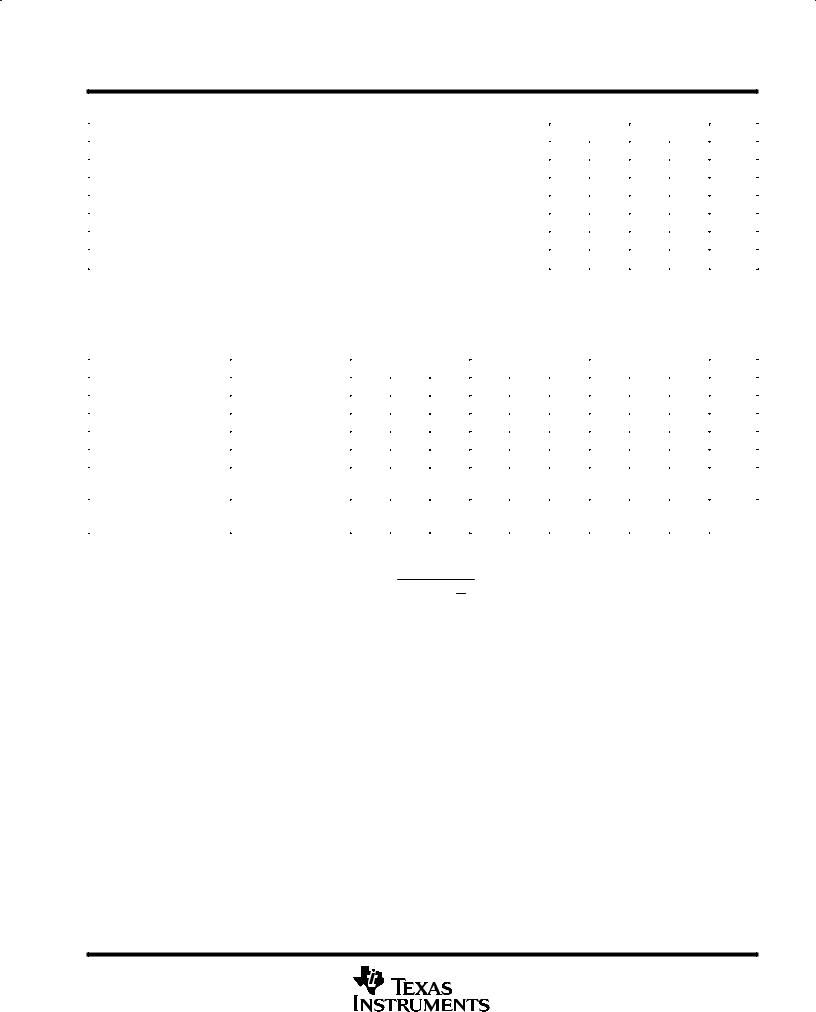
D Complete PWM Power Control Circuitry |
D OR N PACKAGE |
||||||
|
|||||||
D Uncommitted Outputs for Single-Ended or |
|
|
(TOP VIEW) |
||||
Push-Pull Applications |
IN ± |
|
|
|
|
REF OUT |
|
D Low Standby Current . . . 8 mA Typ |
|
1 |
16 |
|
|||
|
|
||||||
D Interchangeable With Silicon General |
IN + |
|
2 |
15 |
|
VCC |
|
|
|
||||||
|
|
|
|
|
|||
SG2524 and SG3524 |
OSC OUT |
|
3 |
14 |
|
EMIT 2 |
|
CURR LIM+ |
|
4 |
13 |
|
COL 2 |
||
|
|
|
|||||
description |
CURR LIM± |
|
5 |
12 |
|
COL 1 |
|
|
|
||||||
The SG2524 and SG3524 incorporate all the |
RT |
|
6 |
11 |
|
EMIT 1 |
|
|
|
||||||
CT |
|
7 |
10 |
|
SHUTDOWN |
||
|
|
||||||
functions required in the construction of a |
GND |
|
8 |
9 |
|
COMP |
|
|
|
||||||
regulating power supply, inverter, or switching |
|
|
|
|
|
|
|
regulator on a single chip. They also can be used |
|
|
|
|
|
|
|
as the control element for high-power-output |
|
|
|
|
|
|
|
applications. The SG2524 and SG3524 were |
|
|
|
|
|
|
|
designed for switching regulators of either polarity, transformer-coupled dc-to-dc converters, transformerless voltage doublers, and polarity converter applications employing fixed-frequency, pulse-width-modulation (PWM) techniques. The complementary output allows either single-ended or push-pull application. Each device includes an on-chip regulator, error amplifier, programmable oscillator, pulse-steering flip-flop, two uncommitted pass transistors, a high-gain comparator, and current-limiting and shut-down circuitry.
The SG2524 is characterized for operation from ±25°C to 85°C, and the SG3524 is characterized for operation from 0°C to 70°C.
AVAILABLE OPTIONS
|
INPUT |
PACKAGED DEVICES |
CHIP FORM |
||
TA |
REGULATION |
SMALL OUTLINE |
PLASTIC DIP |
||
(Y) |
|||||
|
MAX (MV) |
(D) |
(N) |
|
|
|
|
|
|
|
|
0°C to 70°C |
30 |
SG3524D |
SG3524N |
SG3524Y |
|
|
|
|
|
|
|
± 25°C to 85°C |
20 |
SG2524D |
SG2524N |
Ð |
|
|
|
|
|
|
|
The D package is available taped and reeled. Add the suffix R to the device type (e.g., SG3524DR). Chip forms are tested at 25°C.
Please be aware that an important notice concerning availability, standard warranty, and use in critical applications of Texas Instruments semiconductor products and disclaimers thereto appears at the end of this data sheet.
PRODUCTION DATA information is current as of publication date. Products conform to specifications per the terms of Texas Instruments standard warranty. Production processing does not necessarily include testing of all parameters.
Copyright 1999, Texas Instruments Incorporated
POST OFFICE BOX 655303 •DALLAS, TEXAS 75265 |
1 |

SG2524, SG3524
REGULATING PULSE-WIDTH MODULATORS
SLVS077B ± APRIL 1977 ± REVISED JULY 1999
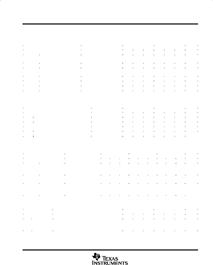
functional block diagram
15 |
Reference |
16 |
VCC |
Regulator |
REF OUT |
|
|
|
|
|
Vref |
RT 6
CT 7
IN ± 1
2
IN+
COMP 9
CURR LIM + 4
5
CURR LIM ±
10
SHUTDOWN
8
GND
|
|
Vref |
12 |
COL 1 |
|
|
|
||
|
|
|
11 |
EMIT 1 |
|
|
T |
13 |
|
|
Vref |
COL 2 |
||
|
|
|
||
|
|
|
14 |
EMIT 2 |
|
Oscillator |
|
3 |
|
|
|
OSC OUT |
||
|
|
|
||
Vref |
|
Vref |
|
|
± |
|
|
|
|
+ |
|
|
Comparator |
|
Error Amplifier
Vref
+
±
1 kΩ
10 kΩ
NOTE A: Resistor values shown are nominal.
absolute maximum ratings over operating free-air temperature range (unless otherwise noted)²
Supply voltage, VCC (see Notes 1 and 2) . . . . . . . . . . . . . . . . . . . . . . . . . . . . . . . . . . . . . . . . . . . |
. . . . . . . . . . 40 V |
Collector output current, ICC . . . . . . . . . . . . . . . . . . . . . . . . . . . . . . . . . . . . . . . . . . . . . . . . . . . . . . . . |
. . . . . . 100 mA |
Reference output current, IO(ref) . . . . . . . . . . . . . . . . . . . . . . . . . . . . . . . . . . . . . . . . . . . . . . . . . . . . |
. . . . . . . 50 mA |
Current through CT terminal . . . . . . . . . . . . . . . . . . . . . . . . . . . . . . . . . . . . . . . . . . . . . . . . . . . . . . . . |
. . . . . . . ±5 mA |
Package thermal impedance, θJA (see Notes 3 and 4): D package . . . . . . . . . . . . . . . . . . . . . |
. . . . . 112°C/W |
N package . . . . . . . . . . . . . . . . . . . . . . |
. . . . . . 88°C/W |
Lead temperature 1,6 mm (1/16 inch) from case for 10 seconds . . . . . . . . . . . . . . . . . . . . . . . . |
. . . . . . . 260°C |
Storage temperature range, Tstg . . . . . . . . . . . . . . . . . . . . . . . . . . . . . . . . . . . . . . . . . . . . . . . . . . . |
± 65°C to 150°C |
²Stresses beyond those listed under ªabsolute maximum ratingsº may cause permanent damage to the device. These are stress ratings only, and functional operation of the device at these or any other conditions beyond those indicated under ªrecommended operating conditionsº is not implied. Exposure to absolute-maximum-rated conditions for extended periods may affect device reliability.
NOTES: 1. All voltage values are with respect to network ground terminal.
2.The reference regulator may be bypassed for operation from a fixed 5-V supply by connecting the VCC and reference output pin both to the supply voltage. In this configuration, the maximum supply voltage is 6 V.
3.Maximum power dissipation is a function of TJ(max), θJA, and TA. The maximum allowable power dissipation at any allowable ambient temperature is PD = (TJ(max) ± TA)/θJA. Operation at the absolute maximum TJ of 150°C can impact reliability.
4.The package thermal impedance is calculated in accordance with JESD 51, except for through-hole packages which use a trace length of zero.
2 |
POST OFFICE BOX 655303 •DALLAS, TEXAS 75265 |
SG2524, SG3524
REGULATING PULSE-WIDTH MODULATORS
SLVS077B ± APRIL 1977 ± REVISED JULY 1999
recommended operating conditions
|
SG2524 |
SG3524 |
UNIT |
||
|
|
|
|
|
|
|
MIN |
MAX |
MIN |
MAX |
|
|
|
||||
|
|
|
|
|
|
Supply voltage, VCC |
8 |
40 |
8 |
40 |
V |
Reference output current |
0 |
50 |
0 |
50 |
mA |
|
|
|
|
|
|
Current through CT terminal |
± 0.03 |
± 2 |
± 0.03 |
± 2 |
mA |
|
|
|
|
|
|
Timing resistor, RT |
1.8 |
100 |
1.8 |
100 |
kΩ |
Timing capacitor, CT |
0.001 |
0.1 |
0.001 |
0.1 |
µF |
Operating free-air temperature |
± 25 |
85 |
0 |
70 |
°C |
|
|
|
|
|
|
electrical characteristics over recommended operating free-air temperature range, VCC = 20 V, f = 20 kHz (unless otherwise noted)
reference section
PARAMETER |
TEST CONDITIONS² |
|
SG2524 |
|
|
SG3524 |
|
SG3524Y |
|
UNIT |
|
|
|
|
|
|
|
|
|
||||
MIN |
TYP³ |
MAX |
MIN |
TYP³ |
MAX |
MIN TYP³ |
MAX |
||||
|
|
|
|||||||||
Output voltage |
|
4.8 |
5 |
5.2 |
4.6 |
5 |
5.4 |
5 |
|
V |
|
|
|
|
|
|
|
|
|
|
|
|
|
Input regulation |
VCC = 8 V to 40 V |
|
10 |
20 |
|
10 |
30 |
10 |
|
mV |
|
Ripple rejection |
f = 120 Hz |
|
66 |
|
|
66 |
|
66 |
|
dB |
|
|
|
|
|
|
|
|
|
|
|
|
|
Output regulation |
IO = 0 mA to 20 mA |
|
20 |
50 |
|
20 |
50 |
20 |
|
mV |
|
Output voltage change |
TA = MIN to MAX |
|
0.3% |
1% |
|
0.3% |
1% |
|
|
|
|
with temperature |
|
|
|
|
|
||||||
|
|
|
|
|
|
|
|
|
|
||
|
|
|
|
|
|
|
|
|
|
|
|
Short-circuit output |
Vref = 0 |
|
100 |
|
|
100 |
|
100 |
|
mA |
|
current§ |
|
|
|
|
|
² For conditions shown as MIN or MAX, use the appropriate value specified under recommended operating conditions. ³ All typical values, except for temperature coefficients, are at TA = 25°C
§ Standard deviation is a measure of the statistical distribution about the mean as derived from the formula:
N
(xn * X)2
n+1
s + N * 1
POST OFFICE BOX 655303 •DALLAS, TEXAS 75265 |
3 |

SG2524, SG3524
REGULATING PULSE-WIDTH MODULATORS
SLVS077B ± APRIL 1977 ± REVISED JULY 1999
electrical characteristics over recommended operating free-air temperature range, VCC = 20 V, f = 20 kHz (unless otherwise noted)
oscillator section
|
|
PARAMETER |
TEST CONDITIONS² |
|
|
|
SG2524, SG3524 |
|
|
SG3524Y |
|
UNIT |
||||||
|
|
|
|
|
|
|
|
|
|
|
|
|||||||
|
|
|
|
|
MIN |
TYP³ |
MAX |
|
MIN |
TYP³ |
MAX |
|||||||
|
|
|
|
|
|
|
|
|
|
|
|
|
||||||
fosc |
Oscillator frequency |
CT = 0.001 µF, |
|
|
RT = 2 kΩ |
|
450 |
|
|
|
450 |
|
kHz |
|||||
|
|
Standard deviation of |
All values of voltage, temperature, |
|
|
|
|
5% |
|
|
|
5% |
|
|
||||
|
|
frequency§ |
resistance, and capacitance constant |
|
|
|
|
|
|
|||||||||
|
|
|
|
|
|
|
|
|
|
|||||||||
|
|
Frequency change with |
VCC = 8 V to 40 V, |
TA = 25°C |
|
|
1% |
|
|
|
1% |
|
||||||
|
|
voltage |
|
|
|
|
|
|
||||||||||
fosc |
|
|
|
|
|
|
|
|
|
|
|
|
|
|
|
|
||
|
|
|
|
|
|
|
|
|
|
|
|
|
|
|
|
|
|
|
|
Frequency change with |
TA = MIN to MAX |
|
|
|
|
|
|
2% |
|
|
|
|
|
||||
|
|
|
|
|
|
|
|
|
|
|
|
|
||||||
|
|
temperature |
|
|
|
|
|
|
|
|
|
|
|
|||||
|
|
|
|
|
|
|
|
|
|
|
|
|
|
|
|
|
||
|
|
|
|
|
|
|
|
|
|
|
|
|
|
|
|
|
|
|
|
|
Output amplitude at OSC |
TA = 25°C |
|
|
|
|
|
|
|
3.5 |
|
|
|
3.5 |
|
V |
|
|
|
OUT |
|
|
|
|
|
|
|
|
|
|
|
|||||
|
|
|
|
|
|
|
|
|
|
|
|
|
|
|
|
|
||
|
|
|
|
|
|
|
|
|
|
|
|
|
|
|
|
|
|
|
tw |
Output pulse duration |
CT = 0.01 µF, |
|
|
TA = 25°C |
|
0.5 |
|
|
|
0.5 |
|
µs |
|||||
(width) at OSC OUT |
|
|
|
|
|
|
|
|||||||||||
|
|
|
|
|
|
|
|
|
|
|
|
|
|
|
|
|
||
|
|
|
|
|
|
|
|
|
|
|
|
|||||||
² For conditions shown as MIN or MAX, use the appropriate value specified under recommended operating conditions. |
|
|
||||||||||||||||
³ All typical values, except for temperature coefficients, are at T |
= 25°C |
|
|
|
|
|
|
|
|
|
|
|
||||||
|
|
|
|
|
|
A |
|
|
|
|
|
|
|
|
|
|
|
|
§ Standard deviation is a measure of the statistical distribution about the mean as derived from the formula: |
|
|
|
|
||||||||||||||
|
|
|
|
|
|
N |
|
|
|
|
|
|
|
|
|
|
|
|
|
|
|
|
|
(xn * |
|
|
|
|
|
|
|
|
|
|
|
||
|
|
|
|
|
X)2 |
|
|
|
|
|
|
|
|
|||||
|
|
|
|
s + |
|
n+1 |
|
|
|
|
|
|
|
|
|
|
|
|
|
|
|
|
N * 1 |
|
|
|
|
|
|
|
|
|
|
|
|||
error amplifier section |
|
|
|
|
|
|
|
|
|
|
|
|
|
|
|
|||
|
|
|
|
|
|
|
|
|
|
|
|
|
|
|
|
|
|
|
|
|
PARAMETER |
|
TEST |
|
SG2524 |
|
|
|
|
SG3524 |
|
|
|
SG3524Y |
|
UNIT |
|
|
|
|
|
|
|
|
|
|
|
|
|
|
|
|
|
|||
|
|
|
CONDITIONS² |
MIN |
TYP³ |
MAX |
MIN |
TYP³ |
MAX |
|
MIN |
TYP³ |
MAX |
|||||
|
|
|
|
|
|
|||||||||||||
VIO |
Input offset voltage |
|
VIC = 2.5 V |
|
|
0.5 |
5 |
|
2 |
10 |
|
|
2 |
|
mV |
|||
IIB |
Input bias current |
|
VIC = 2.5 V |
|
|
2 |
10 |
|
2 |
10 |
|
|
2 |
|
µA |
|||
|
|
Open-loop voltage |
|
|
72 |
|
80 |
|
|
|
60 |
80 |
|
|
|
80 |
|
dB |
|
|
amplification |
|
|
|
|
|
|
|
|
|
|
||||||
|
|
|
|
|
|
|
|
|
|
|
|
|
|
|
|
|
|
|
|
|
|
|
|
|
|
|
|
|
|
|
|
|
|
|
|
|
|
VICR |
Common-mode input |
|
TA = 25°C |
1.8 to |
|
|
|
|
1.8 to |
|
|
|
|
|
|
V |
||
voltage range |
|
3.4 |
|
|
|
|
3.4 |
|
|
|
|
|
|
|||||
|
|
|
|
|
|
|
|
|
|
|
|
|
|
|
||||
|
|
|
|
|
|
|
|
|
|
|
|
|
|
|
|
|
|
|
CMMR |
Common-mode rejection |
|
|
|
|
70 |
|
|
|
|
70 |
|
|
|
70 |
|
dB |
|
ratio |
|
|
|
|
|
|
|
|
|
|
|
|
||||||
|
|
|
|
|
|
|
|
|
|
|
|
|
|
|
|
|
|
|
|
|
|
|
|
|
|
|
|
|
|
|
|
|
|
|
|
|
|
B1 |
Unity-gain bandwidth |
|
|
|
|
3 |
|
|
|
|
3 |
|
|
|
3 |
|
MHz |
|
|
|
Output swing |
|
TA = 25°C |
0.5 |
|
|
3.8 |
0.5 |
|
3.8 |
|
0.5 |
|
3.8 |
V |
||
² For conditions shown as MIN or MAX, use the appropriate value specified under recommended operating conditions. |
|
|
||||||||||||||||
³ All typical values, except for temperature coefficients, are at T |
= 25°C |
|
|
|
|
|
|
|
|
|
|
|
||||||
|
|
|
|
|
|
A |
|
|
|
|
|
|
|
|
|
|
|
|
4 |
POST OFFICE BOX 655303 •DALLAS, TEXAS 75265 |
SG2524, SG3524
REGULATING PULSE-WIDTH MODULATORS
SLVS077B ± APRIL 1977 ± REVISED JULY 1999
electrical characteristics over recommended operating free-air temperature range, VCC = 20 V, f = 20 kHz (unless otherwise noted)
output section
|
PARAMETER |
TEST CONDITIONS² |
SG2534, SG3524 |
SG3524Y |
|
UNIT |
|||
|
|
|
|
|
|
||||
|
MIN |
TYP³ |
MAX |
MIN TYP³ |
MAX |
||||
|
|
|
|
|
|||||
V(BR)CE |
Collector-emitter breakdown |
|
|
40 |
|
|
|
|
V |
voltage |
|
|
|
|
|
|
|||
|
|
|
|
|
|
|
|
|
|
|
|
|
|
|
|
|
|
|
|
|
Collector off-state current |
VCE = 40 V |
|
|
0.01 |
50 |
0.01 |
|
µA |
Vsat |
Collector-emitter saturation |
IC = 50 mA |
|
|
1 |
2 |
1 |
|
V |
voltage |
|
|
|
||||||
|
|
|
|
|
|
|
|
|
|
|
|
|
|
|
|
|
|
|
|
VO |
Emitter output voltage |
VC = 20 V, |
IE = ± 250 µA |
17 |
18 |
|
18 |
|
V |
tr |
Turn-off voltage rise time |
RC = 2 kΩ |
|
|
0.2 |
|
0.2 |
|
µs |
tf |
Turn-on voltage fall time |
RC = 2 kΩ |
|
|
0.1 |
|
0.1 |
|
µs |
² For conditions shown as MIN or MAX, use the appropriate value specified under recommended operating conditions. |
|
|
|||||||
³ All typical values, except for temperature coefficients, are at T |
= 25°C. |
|
|
|
|
|
|
||
|
|
A |
|
|
|
|
|
|
|
comparator section
|
PARAMETER |
TEST CONDITIONS² |
SG2534, SG3524 |
SG3524Y |
|
UNIT |
|
|
|
|
|||
|
MIN TYP³ MAX |
MIN TYP³ |
MAX |
|||
|
|
|
|
|||
|
Maximum duty cycle, each output |
|
45% |
|
|
|
|
|
|
|
|
|
|
VIT |
Input threshold voltage at COMP |
Zero duty cycle |
1 |
1 |
|
V |
|
|
|
|
|||
Maximum duty cycle |
3.5 |
3.5 |
|
|||
|
|
|
|
|||
|
|
|
|
|
|
|
IIB |
Input bias current |
|
± 1 |
± 1 |
|
µA |
² For conditions shown as MIN or MAX, use the appropriate value specified under recommended operating conditions. ³ All typical values, except for temperature coefficients, are at TA = 25°C.
current limiting section
|
PARAMETER |
TEST CONDITIONS |
|
SG2524 |
|
|
SG3524 |
|
|
SG3524Y |
|
UNIT |
|||
|
|
|
|
|
|
|
|
|
|
||||||
|
MIN |
TYP³ |
MAX |
MIN |
TYP² |
MAX |
MIN |
TYP² |
MAX |
||||||
|
|
|
|
|
|
|
|||||||||
|
|
Input voltage |
|
|
|
± 1 |
|
|
± 1 |
|
|
|
|
|
|
VI |
|
range |
|
|
|
to |
|
|
to |
|
|
|
|
|
V |
|
|
(either input) |
|
|
|
1 |
|
|
1 |
|
|
|
|
|
|
|
|
|
|
|
|
|
|
|
|
|
|
|
|
|
|
V(SENSE) |
Sense voltage |
|
|
|
175 |
200 |
225 |
175 |
200 |
225 |
175 |
200 |
225 |
mV |
|
at TA = 25°C |
V |
± V |
≥ 50 mV, |
||||||||||||
|
|
|
|
|
|
|
|
|
|
|
|
|
|||
|
|
Temperature |
(IN +) |
(IN ±) |
|
|
|
|
|
|
|
|
|
|
|
|
|
V(COMP) = 2 V |
|
|
|
|
|
|
|
|
|
|
|
||
|
|
coefficient of |
|
|
0.2 |
|
|
0.2 |
|
|
0.2 |
|
mV/°C |
||
|
|
|
|
|
|
|
|
|
|
|
|||||
|
|
sense voltage |
|
|
|
|
|
|
|
|
|
|
|
|
|
|
|
|
|
|
|
|
|
|
|
|
|||||
³ All typical values, except for temperature coefficients, are at T = 25°C. |
|
|
|
|
|
|
|
|
|||||||
|
|
|
|
|
A |
|
|
|
|
|
|
|
|
|
|
total device
|
PARAMETER |
TEST CONDITIONS |
SG2524, SG3524 |
SG3524Y |
|
UNIT |
||
|
|
|
|
|
|
|||
|
MIN |
TYP³ |
MAX |
MIN TYP³ |
MAX |
|||
|
|
|
|
|||||
|
Standby |
VCC = 40 V, IN ±, CURR LIM +, CT, GND, COMP, |
|
|
|
|
|
|
Ist |
EMIT 1, EMIT 2 grounded, IN + at 2 V, |
|
8 |
10 |
8 |
|
mA |
|
current |
|
|
||||||
|
All other inputs and outputs open |
|
|
|
|
|
|
|
|
|
|
|
|
|
|
|
|
|
|
|
|
|
|
|
|
|
³ All typical values, except for temperature coefficients, are at TA = 25°C.
POST OFFICE BOX 655303 •DALLAS, TEXAS 75265 |
5 |
 Loading...