


Texas Instruments SM320C30HFGM50, SM320C30TBM33, SM320C30GBM33, SM320C30GBM40, SM320C30GBM50 Datasheet
...SMJ320C30 DIGITAL SIGNAL PROCESSOR
SGUS014F ± FEBRUARY 1991 ± REVISED FEBRUARY 1999
2
D ± 55°C to 125°C Operating Temperature
Range, QML Processing
D Processed to MIL-PRF-38535 (QML)
D Performance
± SMJ320C30-40 (50-ns Cycle)
40MFLOPS
20MIPS
±SMJ320C30-50 (40-ns Cycle)
50MFLOPS
25 MIPS
DTwo 1K-Word × 32-Bit Single-Cycle
Dual-Access On-Chip RAM Blocks
DValidated Ada Compiler
D64-Word × 32-Bit Instruction Cache
D32-Bit Instruction and Data Words,
24-Bit Addresses
D40 / 32-Bit Floating-Point /Integer Multiplier and Arithmetic Logic Unit (ALU)
DParallel ALU and Multiplier Execution in a Single Cycle
DOn-Chip Direct Memory Access (DMA) Controller for Concurrent I/O and CPU Operation
DInteger, Floating-Point, and Logical Operations
DOne 4K-Word × 32-Bit Single-Cycle
Dual-Access On-Chip ROM Block
DTwo 32-Bit External Ports (24and 13-Bit Address)
DTwo Serial Ports With Support for 8- / 16- /24- /32-Bit Transfers
DPackaging
±181-Pin Grid Array Ceramic Package (GB Suffix)
±196-Pin Ceramic Quad Flatpack With Nonconductive Tie-Bar (HFG Suffix)
DSMD Approval for 40and 50-MHz Versions
DTwo Address Generators With Eight Auxiliary Registers and Two Auxiliary Register Arithmetic Units (ARAUs)
DZero-Overhead Loops With Single-Cycle Branches
DInterlocked Instructions for Multiprocessing Support
D32-Bit Barrel Shifter
DEight Extended-Precision Registers (Accumulators)
DTwoand Three-Operand Instructions
DConditional Calls and Returns
DBlock Repeat Capability
DFabricated Using Enhanced Performance Implanted CMOS (EPICt) by Texas Instruments (TIt)
DTwo 32-Bit Timers
description
The SMJ320C30 internal busing and special digital signal processor (DSP) instruction set has the speed and flexibility to execute up to 50 MFLOPS. The SMJ320C30 device optimizes speed by implementing functions in hardware that other processors implement through software or microcode. This hardware-intensive approach provides performance previously unavailable on a single chip. The emphasis on total system cost has resulted in a less expensive processor that can be designed into systems currently using costly bit-slice processors.
DSMJ320C30-40: 50-ns single-cycle execution time, 5% supply
DSMJ320C30-50: 40-ns single-cycle execution time, 5% supply
Please be aware that an important notice concerning availability, standard warranty, and use in critical applications of Texas Instruments semiconductor products and disclaimers thereto appears at the end of this data sheet.
EPIC and TI are trademarks of Texas Instruments Incorporated.
PRODUCTION DATA information is current as of publication date. Products conform to specifications per the terms of Texas Instruments standard warranty. Production processing does not necessarily include testing of all parameters.
POST OFFICE BOX 1443 •HOUSTON, TEXAS 77251±1443
Copyright 1998, Texas Instruments Incorporated
On products compliant to MIL-PRF-38535, all parameters are tested unless otherwise noted. On all other products, production processing does not necessarily include testing of all parameters.
1

SMJ320C30
DIGITAL SIGNAL PROCESSOR
SGUS014F ± FEBRUARY 1991 ± REVISED FEBRUARY 1999
181-Pin GB Grid Array Package
( BOTTOM VIEW )
A B C D E F G H J K L M N P R
1
2
3
4
5
6
7
8
9
10
11
12
13
14
15
description (continued)
196-Pin HFG Quad Flatpack
( TOP VIEW )
196 |
148 |
1 |
147 |
DVDD DVSS |
|
|
VDD |
|
VSS |
VSS |
|
VDD |
|
DVSS |
DVDD |
49 |
99 |
50 |
98 |
The SMJ320C30 can perform parallel multiply and ALU operations on integer or floating-point data in a single cycle. Each processor also possesses a general-purpose register file, a program cache, dedicated ARAUs, internal dual-access memories, one DMA channel supporting concurrent I/O, and a short machine-cycle time. High performance and ease of use are results of these features.
General-purpose applications are enhanced by the large address space, multiprocessor interface, internally and externally generated wait states, two external interface ports, two timers, two serial ports, and multiple interrupt structure. The SMJ320C30 supports a wide variety of system applications from host processor to dedicated coprocessor.
High-level language support is implemented easily through a register-based architecture, large address space, powerful addressing modes, flexible instruction set, and well-supported floating-point arithmetic.
2 |
POST OFFICE BOX 1443 •HOUSTON, TEXAS 77251±1443 |

SMJ320C30
DIGITAL SIGNAL PROCESSOR
SGUS014F ± FEBRUARY 1991 ± REVISED FEBRUARY 1999
functional block diagram
RDY
HOLD
HOLDA 
STRB 
 R / W
R / W 
D31± D0 

A23 ± A0 
RESET
INT(3 ± 0)  IACK
IACK
MC / MP
XF(1,0)

VDD IODVDD ADVDD PDVDD DDVDD MDVDD
VSS
DVSS
CVSS
IVSS
VBBP
VSUBS  X1
X1
X2 / CLKIN 
H1
H3 EMU(6 ± 0)
 RSV(10 ± 0)

Cache (64 ×32)
|
32 |
24 |
|
|
PDATA Bus |
||
|
|||
|
PADDR Bus |
||
MUX |
DDATA Bus |
||
DADDR1 Bus |
|||
|
|||
|
DADDR2 Bus |
||
|
DMADATA Bus |
||
|
DMAADDR Bus |
||
|
|
32 |
|
|
|
||
IR
PC
CPU1
Controller
RAM |
|
RAM |
ROM |
||
Block 0 |
|
Block 1 |
Block |
||
(1K |
×32) |
|
(1K ×32) |
(4K |
×32) |
24 |
32 |
24 |
32 |
24 |
32 |
MUX
24 |
|
32 |
|
24 |
24 |
32 |
24 |
|
|
|
|
|
|
|
DMA Controller |
|
|
|
|
|
|
|
Global-Control |
|
|
|
|
|
|
|
Register |
MUX |
|
|
|
|
|
|
|
|
|
|
|
|
|
|
Source-Address |
|
|
|
CPU1 |
|
|
Register |
|
|
|
|
CPU2 |
|
|
Destination- |
|
|
|
|
|
|
|
|
|
|
|
|
REG1 |
|
|
Address |
|
|
|
|
|
|
Register |
||
|
|
|
REG2 |
|
|
Transfer- |
|
|
|
|
|
|
|
|
Counter |
REG1 |
REG2 |
32 |
32 |
40 |
40 |
|
Register |
|
|
||||||
|
|
|
32-Bit |
|
|
||
|
|
Multiplier |
|
Barrel |
|
|
|
|
|
|
|
|
Shifter |
|
|
|
|
40 |
|
|
ALU |
|
|
|
|
|
|
|
|
|
|
|
|
40 |
|
|
|
40 |
|
|
|
|
|
Extended- |
40 |
||
|
|
40 |
|
|
|||
|
|
|
Precision |
|
|
||
|
|
32 |
|
Registers |
40 |
|
|
|
|
|
(R7±R0) |
|
|
||
|
|
|
|
|
|
||
DISP0, IR0, IR1 |
||
ARAU0 |
BK |
ARAU1 |
|
|
|
24 |
|
24 |
|
|
|
24 |
Auxiliary |
24 |
32 |
Registers |
|
(AR0 ± AR7) |
|
|
32 |
|
|
|
32 |
|
|
|
|
32 |
|
|
32 |
Other |
32 |
Registers |
|
|
|
(12) |
|
Peripheral Data Bus |
Peripheral Address Bus |
Serial Port 0
Serial-Port-Control
Register
Receive/Transmit
(R/X) Timer Register
Data-Transmit
Register
Data-Receive
Register
Serial Port 1
Serial-Port-Control
Register
Receive/Transmit
(R/X) Timer Register
Data-Transmit
Register
Data-Receive
Register
Timer 0
Global-Control
Register
Timer-Period
Register
Timer-Counter
Register
Timer 1
Global-Control
Register
Timer-Period
Register
Timer-Counter
Register
Port Control
Primary-Control
Register
Expansion-Control
Register
XRDY
MSTRB
IOSTRB
XR / W XD31±XD0 XA12 ±XA0

 FSX0
FSX0

 DX0
DX0

 CLKX0
CLKX0

 FSR0
FSR0

 DR0
DR0 
 CLKR0
CLKR0

 FSX1
FSX1

 DX1
DX1

 CLKX1
CLKX1

 FSR1
FSR1

 DR1
DR1 
 CLKR1
CLKR1

 TCLK0
TCLK0

 TCLK1
TCLK1
POST OFFICE BOX 1443 •HOUSTON, TEXAS 77251±1443 |
3 |
SMJ320C30
DIGITAL SIGNAL PROCESSOR
SGUS014F ± FEBRUARY 1991 ± REVISED FEBRUARY 1999
memory map
Figure 1 shows the memory map for the SMJ320C30. See the TMS320C3x User's Guide (literature number SPRU031) for a detailed description of this memory mapping. Figure 2 shows the reset, interrupt, and trap vector/branches memory-map locations. Figure 3 shows the peripheral bus memory-mapped registers.
0h
03Fh
040h
7FFFFFh
800000h
801FFFh
802000h
803FFFh
804000h
805FFFh
806000h
807FFFh
808000h
8097FFh
809800h
809BFFh
809C00h
809FFFh
80A000h
Reset, Interrupt, Trap
Vectors, and Reserved
Locations (64) (External
STRB Active)
External
STRB Active
(8M Words ± 64 Words)
Expansion-Bus
MSTRB Active
(8K Words)
Reserved
(8K Words)
Expansion-Bus
IOSTRB Active
(8K Words)
Reserved
(8K Words)
Peripheral-Bus
Memory-Mapped
Registers
(6K Words Internal)
RAM Block 0
(1K Word Internal)
RAM Block 1
(1K Word Internal)
External
STRB Active
(8M Words ± 40K Words)
0h
0BFh
0C0h
0FFFh
1000h
7FFFFFh
800000h
801FFFh
802000h
803FFFh
804000h
805FFFh
806000h
807FFFh
808000h
8097FFh
809800h
809BFFh
809C00h
809FFFh
80A000h
Reset, Interrupt,
Trap Vectors, and Reserved
Locations (192)
ROM (Internal)
External
STRB Active
(8M Words ± 4K Words)
Expansion-Bus
MSTRB Active
(8K Words)
Reserved
(8K Words)
Expansion-Bus
IOSTRB Active
(8K Words)
Reserved
(8K Words)
Peripheral-Bus
Memory-Mapped
Registers
(6K Words Internal)
RAM Block 0
(1K Word Internal)
RAM Block 1
(1K Word Internal)
External
STRB Active
(8M Words ± 40K Words)
0FFFFFFh |
|
0FFFFFFh |
|
|
(a) Microprocessor Mode |
(b) Microcomputer Mode |
|||
|
|
Figure 1. Memory Map
4 |
POST OFFICE BOX 1443 •HOUSTON, TEXAS 77251±1443 |

|
|
|
|
|
|
|
|
SMJ320C30 |
|
|
|
|
|
|
DIGITAL SIGNAL PROCESSOR |
||||
|
|
|
|
|
SGUS014F ± FEBRUARY 1991 ± REVISED FEBRUARY 1999 |
||||
|
|
|
|
|
|
|
|
|
|
memory map (continued) |
|
|
|
|
|
|
|||
|
|
|
|
|
|
|
|
|
|
00h |
Reset |
00h |
Reset |
|
|||||
01h |
|
|
|
01h |
|
|
|
|
|
|
|
|
|
|
|||||
|
INT0 |
|
|
INT0 |
|
|
|||
02h |
|
02h |
|
|
|
|
|||
|
INT1 |
|
|
INT1 |
|
|
|||
03h |
|
|
|
03h |
|
|
|
|
|
|
|
|
|
|
|||||
|
INT2 |
|
|
INT2 |
|
|
|||
04h |
|
04h |
|
|
|
|
|||
|
INT3 |
|
|
INT3 |
|
|
|||
05h |
XINT0 |
05h |
XINT0 |
|
|||||
|
|
|
|
|
|
|
|
|
|
06h |
RINT0 |
06h |
RINT0 |
|
|||||
|
|
|
|
|
|
|
|
|
|
07h |
XINT1 |
07h |
XINT1 |
|
|||||
|
|
|
|
|
|
|
|
|
|
08h |
RINT1 |
08h |
RINT1 |
|
|||||
|
|
|
|
|
|
|
|
|
|
09h |
TINT0 |
09h |
TINT0 |
|
|||||
0Ah |
|
|
|
0Ah |
|
|
|
|
|
TINT1 |
TINT1 |
|
|||||||
0Bh |
|
|
|
0Bh |
|
|
|
|
|
DINT |
DINT |
|
|||||||
0Ch |
|
|
|
0Ch |
|
|
|
|
|
Reserved |
Reserved |
|
|
||||||
1Fh |
1Fh |
|
|||||||
|
|
|
|
|
|
|
|
||
20h |
TRAP 0 |
20h |
TRAP 0 |
|
|||||
|
|
|
|
|
|
|
|
|
|
|
. |
|
|
. |
|
|
|
||
|
. |
|
|
. |
|
|
|
||
|
. |
|
|
. |
|
|
|
||
|
|
|
|
|
|
|
|
|
|
3Bh |
TRAP 27 |
3Bh |
TRAP 27 |
|
|||||
3Ch |
|
|
|
3Ch |
|
|
|
|
|
Reserved |
Reserved |
|
|
||||||
3Fh |
BFh |
|
|||||||
|
|
|
|
|
|
|
|
||
|
(a) Microprocessor Mode |
|
(a) Microcomputer Mode |
||||||
Figure 2. Reset, Interrupt, and Trap Vector/Branches Memory-Map Locations
POST OFFICE BOX 1443 •HOUSTON, TEXAS 77251±1443 |
5 |

SMJ320C30
DIGITAL SIGNAL PROCESSOR
SGUS014F ± FEBRUARY 1991 ± REVISED FEBRUARY 1999
memory map (continued)
808000h |
DMA Global Control |
808004h |
|
|
|
DMA Source Address |
|
808006h |
|
|
|
DMA Destination Address |
|
808008h |
|
|
|
DMA Transfer Counter |
|
808020h |
|
|
|
Timer 0 Global Control |
|
808024h |
|
|
|
Timer 0 Counter |
|
808028h |
|
|
|
Timer 0 Period |
|
808030h |
|
|
|
Timer 1 Global Control |
|
|
|
808034h |
Timer 1 Counter |
|
|
|
|
808038h |
Timer 1 Period Register |
|
|
|
|
808040h |
Serial Port 0 Global Control |
808042h |
|
|
|
FSX/DX/CLKX Serial Port 0 Control |
|
808043h |
FSR/DR/CLKR Serial Port 0 Control |
|
|
808044h |
Serial Port 0 R/X Timer Control |
|
|
808045h |
Serial Port 0 R/X Timer Counter |
|
|
808046h |
Serial Port 0 R/X Timer Period |
|
|
|
|
808048h |
Serial Port 0 Data Transmit |
|
|
|
|
80804Ch |
Serial Port 0 Data Receive |
|
|
|
|
808050h |
Serial Port 1 Global Control |
808052h |
|
|
|
FSX/DX/CLKX Serial Port 1 Control |
|
808053h |
FSR/DR/CLKR Serial Port 1 Control |
808054h |
Serial Port 1 R/X Timer Control |
808055h |
|
Serial Port 1 R/X Timer Counter |
|
808056h |
Serial Port 1 R/X Timer Period |
808058h |
|
|
|
Serial Port 1 Data Transmit |
|
80805Ch |
|
Serial Port 1 Data Receive |
|
808060h |
|
Expansion-Bus Control |
|
|
|
808064h |
Primary-Bus Control |
|
|
|
|
² Shading denotes reserved address locations
Figure 3. Peripheral Bus Memory-Mapped Registers²
6 |
POST OFFICE BOX 1443 •HOUSTON, TEXAS 77251±1443 |

SMJ320C30
DIGITAL SIGNAL PROCESSOR
SGUS014F ± FEBRUARY 1991 ± REVISED FEBRUARY 1999
pin functions
This section gives signal descriptions for the SMJ320C30 devices in the microprocessor mode. The following tables list each signal, the number of pins, type of operating mode(s) (that is, input, output, or high-impedance state as indicated by I, O, or Z, respectively), and a brief function description. All pins labeled NC have special functions and should not be connected by the user. A line over a signal name (for example, RESET) indicates that the signal is active low (true at logic-0 level). The signals are grouped according to functions.
Pin Functions
|
|
|
|
|
|
|
|
|
|
|
|
PIN |
|
|
TYPE² |
|
|
|
|
|
|
|
|
|
|
DESCRIPTION |
|
CONDITIONS |
|
|
|||||||||||||||||
|
NAME |
QTY³ |
|
|
|
|
|
|
|
|
|
|
|
WHEN |
|
|
|||||||||||||||||||||||||||||||
|
|
|
|
|
|
|
|
|
|
|
|
|
|
|
|
|
|
|
|
|
|
|
|
|
|
|
|
|
SIGNAL IS Z TYPE§ |
|
|||||||||||||||||
|
|
|
|
|
|
|
|
|
|
|
|
|
|
|
|
|
|
|
|
|
|
|
|
|
|
PRIMARY BUS INTERFACE |
|
|
|
|
|||||||||||||||||
|
|
|
|
|
|
|
|
|
|
|
|
|
|
|
|
|
|
|
|
|
|
|
|
|
|
|
|
|
|
|
|
|
|
|
|
|
|
|
|
|
|
|
|
|
|
|
|
|
D31 ± D0 |
32 |
|
I / O / Z |
32-bit data port of the primary bus interface |
S |
H |
|
|
||||||||||||||||||||||||||||||||||||||
|
|
|
|
|
|
|
|
|
|
|
|
|
|
|
|
|
|
|
|
|
|
|
|
|
|
|
|
|
|
|
|
|
|
|
|
|
|
|
|
|
|
|
|
|
|
|
|
|
A23± A0 |
24 |
|
O / Z |
24-bit address port of the primary bus interface |
S |
H |
R |
|
||||||||||||||||||||||||||||||||||||||
|
|
|
|
|
|
|
|
|
|
|
|
|
|
|
|
|
|
|
|
|
|
|
|
|
|
|
|
|
|
|
|
|
|
|
|
|
|
|
|
|
|
|
|
|
|
|
|
|
|
|
|
|
|
|
|
|
|
|
|
|
|
|
|
|
|
|
|
|
|
|
|
|
|
|
|
|
|
|
|
|
|
|
|
|
|
|
|
|
|
|
|
|
|
||
|
|
|
|
|
|
|
|
|
|
|
|
|
|
|
|
|
|
Read/ write for primary bus interface. R / |
W |
is high when a read is performed and low |
|
|
|
|
|||||||||||||||||||||||
|
R / W |
1 |
|
O / Z |
S |
H |
R |
|
|||||||||||||||||||||||||||||||||||||||
|
|
when a write is performed over the parallel interface. |
|
||||||||||||||||||||||||||||||||||||||||||||
|
|
|
|
|
|
|
|
|
|
|
|
|
|
|
|
|
|
|
|
|
|
||||||||||||||||||||||||||
|
|
|
|
|
|
|
|
|
|
|
|
|
|
|
|
|
|
|
|
|
|
|
|
|
|
|
|
|
|
|
|
|
|
|
|
|
|
|
|
|
|
|
|
|
|||
|
|
|
|
|
|
|
|
|
|
|
|
|
|
1 |
|
O / Z |
External access strobe for the primary bus interface |
S |
H |
|
|
||||||||||||||||||||||||||
|
STRB |
|
|
|
|
|
|
|
|
|
|
||||||||||||||||||||||||||||||||||||
|
|
|
|
|
|
|
|
|
|
|
|
|
|
|
|
|
|
|
|
|
|
|
|
|
|
|
|
|
|
|
|
|
|
|
|
|
|
|
|
|
|
|
|
||||
|
|
|
|
|
|
|
|
|
|
|
|
|
|
|
|
|
|
Ready. |
|
indicates that the external device is prepared for a primary bus interface |
|
|
|
|
|||||||||||||||||||||||
|
|
|
|
|
|
|
|
|
|
|
|
|
|
|
|
|
|
RDY |
|
|
|
|
|||||||||||||||||||||||||
|
RDY |
1 |
|
I |
|
|
|
|
|||||||||||||||||||||||||||||||||||||||
|
|
transaction to complete. |
|
|
|
|
|||||||||||||||||||||||||||||||||||||||||
|
|
|
|
|
|
|
|
|
|
|
|
|
|
|
|
|
|
|
|
|
|
||||||||||||||||||||||||||
|
|
|
|
|
|
|
|
|
|
|
|
|
|
|
|
|
|
|
|
|
|
|
|
|
|
|
|
|
|
|
|
|
|
|
|
|
|
|
|
|
|
||||||
|
|
|
|
|
|
|
|
|
|
|
|
|
|
|
|
|
|
Hold for primary bus interface. When |
|
|
|
|
is a logic low, any ongoing transaction |
|
|
|
|
||||||||||||||||||||
|
|
|
|
|
|
|
|
|
|
|
|
|
|
|
|
|
|
HOLD |
|
|
|
|
|||||||||||||||||||||||||
|
|
|
|
|
|
|
|
|
|
|
|
|
|
|
|
|
|
is completed. A23 ± A0, D31 ± D0, STRB, and R / W are in the high-impedance state |
|
|
|
|
|||||||||||||||||||||||||
|
HOLD |
1 |
|
I |
|
|
|
|
|||||||||||||||||||||||||||||||||||||||
|
|
and all transactions over the primary bus interface are held until HOLD becomes a |
|
|
|
|
|||||||||||||||||||||||||||||||||||||||||
|
|
|
|
|
|
|
|
|
|
|
|
|
|
|
|
|
|
|
|
|
|
||||||||||||||||||||||||||
|
|
|
|
|
|
|
|
|
|
|
|
|
|
|
|
|
|
logic high or the NOHOLD bit of the primary bus control register is set. |
|
|
|
|
|||||||||||||||||||||||||
|
|
|
|
|
|
|
|
|
|
|
|
|
|
|
|
|
|
|
|
|
|
|
|
|
|
|
|
|
|
|
|
|
|
|
|
|
|
|
|
|
|
||||||
|
|
|
|
|
|
|
|
|
|
|
|
|
|
|
|
|
|
|
|
|
|
|
|
|
|
|
|
|
|
|
|
|
|
|
|
|
|
|
|
||||||||
|
|
|
|
|
|
|
|
|
|
|
|
|
|
|
|
|
|
Hold acknowledge for primary bus interface. |
HOLDA |
is generated in response to a |
|
|
|
|
|||||||||||||||||||||||
|
|
|
|
|
|
|
|
|
|
|
|
|
|
|
|
|
|
logic low on HOLD. HOLDA indicates that A23 ± A0, D31 ± D0, STRB, and R / W are |
|
|
|
|
|||||||||||||||||||||||||
|
HOLDA |
|
|
|
|
|
1 |
|
O / Z |
in the high-impedance state and that all transactions over the bus are held. |
HOLDA |
|
S |
|
|
|
|||||||||||||||||||||||||||||||
|
|
|
|
|
|
|
|
|
|
|
|
|
|
|
|
|
|
is high in response to a logic high of |
HOLD |
or when the NOHOLD bit of the primary |
|
|
|
|
|||||||||||||||||||||||
|
|
|
|
|
|
|
|
|
|
|
|
|
|
|
|
|
|
bus control register is set. |
|
|
|
|
|||||||||||||||||||||||||
|
|
|
|
|
|
|
|
|
|
|
|
|
|
|
|
|
|
|
|
|
|
|
|
|
|
|
|
|
|
|
|
|
|
|
|
|
|
|
|
|
|
|
|
|
|
|
|
|
|
|
|
|
|
|
|
|
|
|
|
|
|
|
|
|
|
|
|
|
|
|
|
EXPANSION BUS INTERFACE |
|
|
|
|
|||||||||||||||||||
|
|
|
|
|
|
|
|
|
|
|
|
|
|
|
|
|
|
|
|
|
|
|
|
|
|
|
|
|
|
|
|
|
|
||||||||||||||
|
XD31± XD0 |
32 |
|
I / O / Z |
32-bit data port of the expansion bus interface |
S |
|
R |
|
||||||||||||||||||||||||||||||||||||||
|
|
|
|
|
|
|
|
|
|
|
|
|
|
|
|
|
|
|
|
|
|
|
|
|
|
|
|
|
|
|
|
|
|
||||||||||||||
|
XA12± XA0 |
13 |
|
O / Z |
13-bit address port of the expansion bus interface |
S |
|
R |
|
||||||||||||||||||||||||||||||||||||||
|
|
|
|
|
|
|
|
|
|
|
|
|
|
|
|
|
|
|
|
|
|
|
|
|
|
|
|
|
|
|
|
|
|
||||||||||||||
|
|
|
|
|
|
|
|
|
|
|
|
|
|
|
|
|
|
Read/ write signal for expansion bus interface. When a read is performed, XR / |
|
|
is |
|
|
|
|
||||||||||||||||||||||
|
|
|
|
|
|
|
|
|
|
|
|
|
|
|
|
|
|
W |
|
|
|
|
|||||||||||||||||||||||||
|
XR / W |
1 |
|
O / Z |
S |
|
R |
|
|||||||||||||||||||||||||||||||||||||||
|
|
held high; when a write is performed, XR / W is low. |
|
|
|||||||||||||||||||||||||||||||||||||||||||
|
|
|
|
|
|
|
|
|
|
|
|
|
|
|
|
|
|
|
|
|
|
||||||||||||||||||||||||||
|
|
|
|
|
|
|
|
|
|
|
|
|
|
|
|
|
|
|
|
|
|
|
|
|
|
|
|
|
|
||||||||||||||||||
|
|
|
|
|
|
|
|
|
|
|
|
|
|
1 |
|
O / Z |
External memory access strobe for the expansion bus interface |
S |
|
|
|
||||||||||||||||||||||||||
|
MSTRB |
|
|
|
|
|
|
|
|
||||||||||||||||||||||||||||||||||||||
|
|
|
|
|
|
|
|
|
|
|
|
|
|
|
|
|
|
|
|
|
|
|
|
|
|
|
|
|
|||||||||||||||||||
|
|
|
|
|
|
|
|
|
|
|
|
|
|
1 |
|
O / Z |
External I / O access strobe for the expansion bus interface |
S |
|
|
|
||||||||||||||||||||||||||
|
IOSTRB |
|
|
|
|
|
|
||||||||||||||||||||||||||||||||||||||||
|
|
|
|
|
|
|
|
|
|
|
|
|
|
|
|
|
|
|
|
|
|
|
|
|
|
|
|
|
|
|
|
|
|
||||||||||||||
|
|
|
|
|
|
|
|
|
|
|
|
|
|
|
|
|
|
|
|
|
|
|
|
|
|
|
|
|
|
|
|
||||||||||||||||
|
|
|
|
|
|
|
|
|
|
|
|
|
|
|
|
|
|
Ready signal. |
XRDY |
|
indicates that the external device is prepared for an expansion |
|
|
|
|
||||||||||||||||||||||
|
XRDY |
1 |
|
I |
|
|
|
|
|||||||||||||||||||||||||||||||||||||||
|
|
bus interface transaction to complete. |
|
|
|
|
|||||||||||||||||||||||||||||||||||||||||
|
|
|
|
|
|
|
|
|
|
|
|
|
|
|
|
|
|
|
|
|
|
||||||||||||||||||||||||||
|
|
|
|
|
|
|
|
|
|
|
|
|
|
|
|
|
|
|
|
|
|
|
|
|
|
|
|
|
|
|
|
|
|
|
|
|
|
||||||||||
|
|
|
|
|
|
|
|
|
|
|
|
|
|
|
|
|
|
|
|
|
|
|
|
|
|
|
CONTROL SIGNALS |
|
|
|
|
||||||||||||||||
|
|
|
|
|
|
|
|
|
|
|
|
|
|
|
|
|
|
|
|
|
|
|
|
|
|
|
|
|
|
|
|
||||||||||||||||
|
|
|
|
|
|
|
|
|
|
|
|
|
|
|
|
|
|
Reset. When |
RESET |
is a logic low, the device is in the reset condition. When |
RESET |
|
|
|
|
|
|||||||||||||||||||||
|
RESET |
1 |
|
I |
|
|
|
|
|||||||||||||||||||||||||||||||||||||||
|
|
becomes a logic high, execution begins from the location specified by the reset vector. |
|
|
|
|
|||||||||||||||||||||||||||||||||||||||||
|
|
|
|
|
|
|
|
|
|
|
|
|
|
|
|
|
|
|
|
|
|
||||||||||||||||||||||||||
|
|
|
|
|
|
|
|
|
|
|
|
|
|
|
|
|
|
|
|
|
|
||||||||||||||||||||||||||
|
|
|
|
|
± |
|
|
|
|
|
|
4 |
|
I |
External interrupts |
|
|
|
|
||||||||||||||||||||||||||||
|
INT3 |
INT0 |
|
|
|
|
|
|
|||||||||||||||||||||||||||||||||||||||
|
|
|
|
|
|
|
|
|
|
|
|
|
|
|
|
|
|
|
|
|
|
|
|
|
|
|
|
|
|||||||||||||||||||
|
|
|
|
|
|
|
|
|
|
|
|
|
|
|
|
|
|
|
|
|
|
|
|
|
|
|
|||||||||||||||||||||
|
|
|
|
|
|
|
|
|
|
|
|
|
|
|
|
|
|
Interrupt acknowledge. |
IACK |
is set to a logic high by the IACK instruction. |
IACK |
can |
|
|
|
|
|||||||||||||||||||||
|
IACK |
1 |
|
O / Z |
S |
|
|
|
|||||||||||||||||||||||||||||||||||||||
|
|
be used to indicate the beginning or end of an interrupt-service routine. |
|
|
|
||||||||||||||||||||||||||||||||||||||||||
|
|
|
|
|
|
|
|
|
|
|
|
|
|
|
|
|
|
|
|
|
|
||||||||||||||||||||||||||
|
|
|
|
|
|
|
|
|
|
|
|
|
|||||||||||||||||||||||||||||||||||
|
MC / |
|
|
|
|
|
|
|
|
|
|
1 |
|
I |
Microcomputer/ microprocessor mode |
|
|
|
|
||||||||||||||||||||||||||||
|
MP |
|
|
|
|
|
|
||||||||||||||||||||||||||||||||||||||||
|
|
|
|
|
|
|
|
|
|
|
|
|
|
|
|
|
|
|
|
|
|
|
|
|
|||||||||||||||||||||||
|
XF1, XF0 |
2 |
|
I / O / Z |
External flags. XF1 and XF0 are used as general-purpose I / Os or to support |
S |
|
R |
|
||||||||||||||||||||||||||||||||||||||
|
|
interlocked processor instructions. |
|
|
|||||||||||||||||||||||||||||||||||||||||||
|
|
|
|
|
|
|
|
|
|
|
|
|
|
|
|
|
|
|
|
|
|
||||||||||||||||||||||||||
|
|
|
|
|
|
|
|
|
|
|
|
|
|
|
|
|
|
|
|
|
|
|
|
|
|
|
|
|
|
|
|
|
|
|
|
|
|
|
|
|
|
|
|
|
|
|
|
² I = input, O = output, Z = high-impedance state, NC = no connect |
|
|
|
|
|||||||||||||||||||||||||||||||||||||||||||
³ For GB package |
|
|
|
|
|
|
|
|
|
|
|
|
|
|
|
|
|
|
|
|
|
|
|
|
|
|
|
|
|
|
|
|
|||||||||||||||
§ S = SHZ active, H = |
HOLD |
active, R = |
RESET |
active |
|
|
|
|
|||||||||||||||||||||||||||||||||||||||
|
|
|
|
|
|
|
|
|
|
|
|
|
|
|
|
|
|
|
|
|
|
|
|
|
|
|
|
|
|
|
|
|
|
|
|
|
|
|
|
|
|
|
|
|
|
|
|
|
|
|
|
|
|
|
|
|
|
|
|
|
|
|
|
|
|
|
|
|
|
|
|
|
|
|
|
|
|
|
|
|
|
|
|
|
|
|
|
|
|
|
|
|
|
|
|
POST OFFICE BOX 1443 •HOUSTON, TEXAS 77251±1443 |
7 |

SMJ320C30
DIGITAL SIGNAL PROCESSOR
SGUS014F ± FEBRUARY 1991 ± REVISED FEBRUARY 1999
Pin Functions (Continued)
|
PIN |
TYPE² |
DESCRIPTION |
|
CONDITIONS |
|
NAME |
QTY³ |
|
WHEN |
|||
|
|
SIGNAL IS Z TYPE§ |
||||
|
|
|
SERIAL PORT 0 SIGNALS |
|
|
|
|
|
|
|
|
|
|
CLKX0 |
1 |
I / O / Z |
Serial port 0 transmit clock. CLKX0 is the serial-shift clock for the serial port 0 |
S |
R |
|
transmitter. |
||||||
|
|
|
|
|
||
|
|
|
|
|
|
|
DX0 |
1 |
I / O / Z |
Data transmit output. Serial port 0 transmits serial data on DX0. |
S |
R |
|
|
|
|
|
|
|
|
FSX0 |
1 |
I / O / Z |
Frame synchronization pulse for transmit. The FSX0 pulse initiates the transmit-data |
S |
R |
|
process over DX0. |
||||||
|
|
|
|
|
||
|
|
|
|
|
|
|
CLKR0 |
1 |
I / O / Z |
Serial port 0 receive clock. CLKR0 is the serial-shift clock for the serial port 0 receiver. |
S |
R |
|
|
|
|
|
|
|
|
DR0 |
1 |
I / O / Z |
Data receive. Serial port 0 receives serial data on DR0. |
S |
R |
|
|
|
|
|
|
|
|
FSR0 |
1 |
I / O / Z |
Frame synchronization pulse for receive. The FSR0 pulse initiates the receive-data |
S |
R |
|
process over DR0. |
||||||
|
|
|
|
|
||
|
|
|
|
|
|
|
|
|
|
SERIAL PORT 1 SIGNALS |
|
|
|
|
|
|
|
|
|
|
CLKX1 |
1 |
I / O / Z |
Serial port 1 transmit clock. CLKX1 is the serial-shift clock for the serial port 1 |
S |
R |
|
transmitter. |
||||||
|
|
|
|
|
||
|
|
|
|
|
|
|
DX1 |
1 |
I / O / Z |
Data transmit output. Serial port 1 transmits serial data on DX1. |
S |
R |
|
|
|
|
|
|
|
|
FSX1 |
1 |
I / O / Z |
Frame synchronization pulse for transmit. The FSX1 pulse initiates the transmit-data |
S |
R |
|
process over DX1. |
||||||
|
|
|
|
|
||
|
|
|
|
|
|
|
CLKR1 |
1 |
I / O / Z |
Serial port 1 receive clock. CLKR1 is the serial-shift clock for the serial port 1 receiver. |
S |
R |
|
|
|
|
|
|
|
|
DR1 |
1 |
I / O / Z |
Data receive. Serial port 1 receives serial data on DR1. |
S |
R |
|
|
|
|
|
|
|
|
FSR1 |
1 |
I / O / Z |
Frame synchronization pulse for receive. The FSR1 pulse initiates the receive-data |
S |
R |
|
process over DR1. |
||||||
|
|
|
|
|
||
|
|
|
|
|
|
|
|
|
|
TIMER 0 SIGNALS |
|
|
|
|
|
|
|
|
|
|
TCLK0 |
1 |
I / O / Z |
Timer clock 0. As an input, TCLK0 is used by timer 0 to count external pulses. As an |
S |
R |
|
output, TCLK0 outputs pulses generated by timer 0. |
||||||
|
|
|
|
|
||
|
|
|
|
|
|
|
|
|
|
TIMER 1 SIGNALS |
|
|
|
|
|
|
|
|
|
|
TCLK1 |
1 |
I / O / Z |
Timer clock 1. As an input, TCLK1 is used by timer 1 to count external pulses. As an |
S |
R |
|
output, TCLK1 outputs pulses generated by timer 1. |
||||||
|
|
|
|
|
||
|
|
|
|
|
|
|
|
|
|
SUPPLY AND OSCILLATOR SIGNALS (see Note 1) |
|
|
|
|
|
|
|
|
|
|
V |
4 |
I |
5-V supply¶ |
|
|
|
DD |
|
|
|
|
|
|
IODVDD |
2 |
I |
5-V supply¶ |
|
|
|
ADVDD |
2 |
I |
5-V supply¶ |
|
|
|
PDVDD |
1 |
I |
5-V supply¶ |
|
|
|
DDVDD |
2 |
I |
5-V supply¶ |
|
|
|
MDV |
1 |
I |
5-V supply¶ |
|
|
|
DD |
|
|
|
|
|
|
VSS |
4 |
I |
Ground |
|
|
|
DVSS |
4 |
I |
Ground |
|
|
|
CVSS |
2 |
I |
Ground |
|
|
|
² I = input, O = output, Z = high-impedance state, NC = no connect ³ For GB package
§ S = SHZ active, H = HOLD active, R = RESET active ¶ Recommended decoupling capacitor is 0.1 F.
NOTE 1: CVSS, VSS, and IVSS are on the same plane.
8 |
POST OFFICE BOX 1443 •HOUSTON, TEXAS 77251±1443 |

|
|
|
|
|
|
|
|
SMJ320C30 |
|
|
|
|
|
|
|
|
DIGITAL SIGNAL PROCESSOR |
||
|
|
|
|
|
|
SGUS014F ± FEBRUARY 1991 ± REVISED FEBRUARY 1999 |
|||
|
|
|
|
|
|
|
|
|
|
|
|
|
|
|
Pin Functions (Continued) |
|
|
||
|
|
|
|
|
|
|
|
|
|
|
PIN |
|
TYPE² |
DESCRIPTION |
CONDITIONS |
|
|||
NAME |
QTY³ |
WHEN |
|
||||||
|
|
|
|
SIGNAL IS Z TYPE§ |
|
||||
|
|
|
|
|
SUPPLY AND OSCILLATOR SIGNALS (see Note 1) (CONTINUED) |
|
|
||
|
|
|
|
|
|
|
|
|
|
IVSS |
1 |
I |
Ground |
|
|
||||
VBBP |
1 |
NC |
VBB pump oscillator output |
|
|
||||
VSUBS |
1 |
I |
Substrate pin. Tie to ground |
|
|
||||
X1 |
1 |
O |
Output from the internal oscillator for the crystal. If a crystal is not used, X1 must |
|
|
||||
be left unconnected. |
|
|
|||||||
|
|
|
|
|
|
|
|||
|
|
|
|
|
|
|
|
|
|
X2 / CLKIN |
1 |
I |
Input to the internal oscillator from the crystal or a clock |
|
|
||||
|
|
|
|
|
|
|
|
|
|
H1 |
1 |
O / Z |
External H1 clock. H1 has a period equal to twice CLKIN. |
S |
|
||||
|
|
|
|
|
|
|
|
|
|
H3 |
1 |
O / Z |
External H3 clock. H3 has a period equal to twice CLKIN. |
S |
|
||||
|
|
|
|
|
|
|
|
|
|
|
|
|
|
|
RESERVED (see Note 2) |
|
|
||
|
|
|
|
|
|
|
|
|
|
EMU0± EMU2 |
3 |
I |
Reserved. Use pullup resistors to 5 V |
|
|
||||
|
|
|
|
|
|
|
|
|
|
EMU3 |
1 |
O / Z |
Reserved |
S |
|
||||
|
|
|
|
|
|
|
|
||
|
|
|
|
|
Shutdown high impedance. When active, EMU4 / |
|
shuts down the SMJ320C30 |
|
|
|
|
|
|
|
SHZ |
|
|
||
|
|
|
|
|
and places all pins in the high-impedance state. EMU4 / SHZ is used for board-level |
|
|
||
EMU4/ |
SHZ |
|
1 |
I |
testing to ensure that no dual-drive conditions occur. CAUTION: A low on SHZ |
|
|
||
|
|
|
|
|
corrupts SMJ320C30 memory and register contents. Reset the device with SHZ |
|
|
||
|
|
|
|
|
high to restore it to a known operating condition. |
|
|
||
|
|
|
|
|
|
||||
EMU5, EMU6 |
2 |
NC |
Reserved |
|
|
||||
|
|
|
|
|
|
||||
RSV0 ± RSV4 |
5 |
I |
Reserved. Tie pins directly to 5 V |
|
|
||||
|
|
|
|
|
|
||||
RSV5 ± RSV10 |
6 |
I / O |
Reserved. Use pullups on each pin to 5 V |
|
|
||||
|
|
|
|
|
|
||||
Locator |
1 |
NC |
Reserved |
|
|
||||
² I = input, O = output, Z = high-impedance state, NC = No Connect ³ For GB package
§ S = SHZ active, H = HOLD active, R = RESET active NOTES: 1. CVSS, VSS, IVSS are on the same plane.
2.The connections specified for the reserved pins must be followed. For best results, 18-kΩ ± 22-kΩ pullup resistors are recommended. All 5-V supply pins must be connected to a common supply plane, and all ground pins must be connected to a common ground plane.
POST OFFICE BOX 1443 •HOUSTON, TEXAS 77251±1443 |
9 |

SMJ320C30
DIGITAL SIGNAL PROCESSOR
SGUS014F ± FEBRUARY 1991 ± REVISED FEBRUARY 1999
Pin Assignments
|
|
PIN |
|
PIN |
|
|
|
|
|
|
|
PIN |
|
PIN |
|
|
PIN |
|
|||||||||||||||||
|
|
|
|
|
|
|
|
|
|
|
|
|
|
|
|
|
|
|
|
|
|
|
|
|
|
|
|
|
|
|
|
|
|
|
|
NUMBER |
|
|
|
|
|
|
|
|
|
|
|
|
|
|
NUMBER |
|
|
|
|
|
|
NUMBER |
|
|
|
NUMBER |
|
|
NUMBER |
|
|||||
|
|
|
|
|
|
NAME |
|
|
|
NAME |
|
|
NAME |
|
|
|
NAME |
|
|
NAME |
|||||||||||||||
GB |
HFG |
|
GB |
HFG |
GB |
HFG |
GB |
HFG |
|
GB |
HFG |
||||||||||||||||||||||||
PKG |
PKG |
|
|
|
|
|
|
|
|
|
|
|
|
|
|
PKG |
PKG |
|
|
|
|
|
|
PKG |
PKG |
|
|
|
PKG |
PKG |
|
|
PKG |
PKG |
|
|
|
|
|
|
|
|
|
|
|
|
|
|
|
|
|
|
|
||||||||||||||||||
F15 |
82 |
|
|
A0 |
C5 |
139 |
D5 |
P2 |
195 |
DX1 |
L2 |
185 |
|
RSV6 |
R8 |
29 |
XD11 |
||||||||||||||||||
G12 |
81 |
|
|
A1 |
D6 |
138 |
D6 |
F14 |
83 |
EMU0 |
K4 |
186 |
|
RSV7 |
R9 |
30 |
XD12 |
||||||||||||||||||
G13 |
80 |
|
|
A2 |
A4 |
137 |
D7 |
E15 |
84 |
EMU1 |
M1 |
187 |
|
RSV8 |
P9 |
31 |
XD13 |
||||||||||||||||||
G14 |
79 |
|
|
A3 |
B5 |
136 |
D8 |
F13 |
85 |
EMU2 |
L3 |
188 |
|
RSV9 |
N9 |
32 |
XD14 |
||||||||||||||||||
G15 |
78 |
|
|
A4 |
C6 |
135 |
D9 |
E14 |
86 |
EMU3 |
M2 |
189 |
|
RSV10 |
R10 |
33 |
XD15 |
||||||||||||||||||
H15 |
77 |
|
|
A5 |
A5 |
134 |
D10 |
F12 |
87 |
EMU4 / |
|
|
D12 |
100 |
|
ADVDD{ |
M9 |
34 |
XD16 |
||||||||||||||||
|
|
SHZ |
|
||||||||||||||||||||||||||||||||
H14 |
72 |
|
|
A6 |
B6 |
133 |
D11 |
C1 |
155 |
EMU5 |
H11 |
64 |
|
ADVDD{ |
P10 |
35 |
XD17 |
||||||||||||||||||
J15 |
71 |
|
|
A7 |
D7 |
132 |
D12 |
M6 |
11 |
EMU6 |
D4 |
114 |
|
DDVDD{ |
R11 |
36 |
XD18 |
||||||||||||||||||
J14 |
70 |
|
|
A8 |
A6 |
131 |
D13 |
B3 |
145 |
H1 |
E8 |
147 |
|
DDVDD{ |
N10 |
37 |
XD19 |
||||||||||||||||||
J13 |
69 |
|
|
A9 |
C7 |
130 |
D14 |
A1 |
146 |
H3 |
L8 |
15 |
|
IODVDD{ |
P11 |
38 |
XD20 |
||||||||||||||||||
K15 |
68 |
|
|
A10 |
B7 |
129 |
D15 |
C2 |
152 |
X1 |
M12 |
16 |
|
IODVDD{ |
R12 |
39 |
XD21 |
||||||||||||||||||
J12 |
67 |
|
|
A11 |
A7 |
128 |
D16 |
B1 |
151 |
X2 / CLKIN |
|
49 |
|
IODVDD{ |
M10 |
40 |
XD22 |
||||||||||||||||||
K14 |
66 |
|
|
A12 |
A8 |
127 |
D17 |
P4 |
9 |
TCLK0 |
H5 |
162 |
|
MDVDD{ |
N11 |
41 |
XD23 |
||||||||||||||||||
L15 |
65 |
|
|
A13 |
B8 |
122 |
D18 |
N5 |
10 |
TCLK1 |
|
163 |
|
MDVDD{ |
P12 |
42 |
XD24 |
||||||||||||||||||
K13 |
63 |
|
|
A14 |
A9 |
121 |
D19 |
G2 |
169 |
XF0 |
M4 |
1 |
|
PDVDD{ |
R13 |
43 |
XD25 |
||||||||||||||||||
L14 |
62 |
|
|
A15 |
B9 |
120 |
D20 |
G3 |
168 |
XF1 |
B2 |
51 |
|
CVSSw |
R14 |
44 |
XD26 |
||||||||||||||||||
M15 |
61 |
|
|
A16 |
C9 |
119 |
D21 |
D3 |
154 |
VBBP |
P14 |
52 |
|
CVSSw |
M11 |
45 |
XD27 |
||||||||||||||||||
K12 |
60 |
|
|
A17 |
A10 |
118 |
D22 |
E4 |
153 |
VSUBS |
|
25 |
|
VDD} |
N12 |
46 |
XD28 |
||||||||||||||||||
L13 |
59 |
|
|
A18 |
D9 |
117 |
D23 |
H4 |
123 |
VDD} |
|
26 |
|
VDD} |
P13 |
47 |
XD29 |
||||||||||||||||||
M14 |
58 |
|
|
A19 |
B10 |
116 |
D24 |
D8 |
73 |
VDD} |
|
172 |
|
VDD} |
R15 |
48 |
XD30 |
||||||||||||||||||
N15 |
57 |
|
|
A20 |
A11 |
115 |
D25 |
M8 |
74 |
VDD} |
|
173 |
|
VDD} |
P15 |
53 |
XD31 |
||||||||||||||||||
M13 |
56 |
|
|
A21 |
C10 |
113 |
D26 |
H12 |
124 |
VDD} |
C8 |
28 |
|
VSSw |
|
2 |
DVDD |
||||||||||||||||||
L12 |
55 |
|
|
A22 |
B11 |
112 |
D27 |
N8 |
27 |
VSSw |
H3 |
75 |
|
VSSw |
|
101 |
DVDD |
||||||||||||||||||
N14 |
54 |
|
|
A23 |
A12 |
111 |
D28 |
A13 |
107 |
XA0 |
H13 |
76 |
|
VSSw |
C3 |
50 |
DVSSW |
||||||||||||||||||
E5 |
|
|
|
LOCATOR/NC |
D10 |
110 |
D29 |
A14 |
106 |
XA1 |
|
125 |
|
VSSw |
C13 |
98 |
DVSSW |
||||||||||||||||||
G1 |
170 |
|
|
|
|
|
|
|
|
|
|
|
|
|
|
C11 |
109 |
D30 |
D11 |
105 |
XA2 |
|
126 |
|
VSSw |
N3 |
148 |
DVSSW |
|||||||
|
|
IACK |
|
|
|||||||||||||||||||||||||||||||
H2 |
171 |
|
|
|
|
|
|
|
|
|
|
|
|
|
B12 |
108 |
D31 |
C12 |
104 |
XA3 |
|
149 |
|
VSSw |
N13 |
196 |
DVSSW |
||||||||
|
|
INT0 |
|
|
|||||||||||||||||||||||||||||||
H1 |
176 |
|
|
|
|
|
|
|
|
|
|
|
|
|
F3 |
161 |
|
|
|
|
|
|
B13 |
103 |
XA4 |
|
150 |
|
VSSw |
B14 |
96 |
IVSSw |
|||
|
|
INT1 |
HOLD |
|
|
||||||||||||||||||||||||||||||
J1 |
177 |
|
|
|
|
|
|
|
|
|
|
|
|
|
E2 |
160 |
|
|
|
|
|
A15 |
102 |
XA5 |
|
174 |
|
VSSw |
|
97 |
IVSSw |
||||
|
|
INT2 |
HOLDA |
|
|
|
|||||||||||||||||||||||||||||
J2 |
178 |
|
|
|
|
|
|
|
|
|
|
|
|
|
D2 |
156 |
|
|
|
|
|
B15 |
95 |
XA6 |
|
175 |
|
VSSw |
|
|
|
||||
|
|
INT3 |
XRDY |
|
|
|
|
|
|||||||||||||||||||||||||||
D15 |
88 |
|
|
MC / |
|
|
|
|
|
|
|
D1 |
159 |
XR / |
|
|
C14 |
94 |
XA7 |
|
99 |
|
VSUBS |
|
|
|
|||||||||
|
|
MP |
W |
|
|
|
|
|
|||||||||||||||||||||||||||
E3 |
157 |
|
|
|
|
|
|
|
|
|
|
P3 |
4 |
FSR0 |
E12 |
93 |
XA8 |
R4 |
12 |
|
XD0 |
|
|
|
|||||||||||
|
|
MSTRB |
|
|
|
|
|||||||||||||||||||||||||||||
E1 |
164 |
|
|
|
|
|
|
|
|
R2 |
7 |
FSX0 |
D13 |
92 |
XA9 |
P5 |
13 |
|
XD1 |
|
|
|
|||||||||||||
|
|
RDY |
|
|
|
|
|||||||||||||||||||||||||||||
F1 |
167 |
|
|
|
|
|
|
|
N4 |
5 |
CLKR0 |
C15 |
91 |
XA10 |
N6 |
14 |
|
XD2 |
|
|
|
||||||||||||||
|
|
RESET |
|
|
|
|
|||||||||||||||||||||||||||||
G4 |
166 |
|
|
R / |
|
|
|
|
M5 |
6 |
CLKX0 |
D14 |
90 |
XA11 |
R5 |
17 |
|
XD3 |
|
|
|
||||||||||||||
|
|
W |
|
|
|
|
|||||||||||||||||||||||||||||
F2 |
165 |
|
|
|
|
|
|
R1 |
3 |
DR0 |
E13 |
89 |
XA12 |
P6 |
18 |
|
XD4 |
|
|
|
|||||||||||||||
|
|
STRB |
|
|
|
|
|||||||||||||||||||||||||||||
F4 |
158 |
|
|
|
|
R3 |
8 |
DX0 |
J3 |
179 |
RSV0 |
M7 |
19 |
|
XD5 |
|
|
|
|||||||||||||||||
|
|
IOSTRB |
|
|
|
|
|||||||||||||||||||||||||||||
C4 |
144 |
|
|
D0 |
M3 |
191 |
FSR1 |
J4 |
180 |
RSV1 |
R6 |
20 |
|
XD6 |
|
|
|
||||||||||||||||||
D5 |
143 |
|
|
D1 |
P1 |
194 |
FSX1 |
K1 |
181 |
RSV2 |
N7 |
21 |
|
XD7 |
|
|
|
||||||||||||||||||
A2 |
142 |
|
|
D2 |
L4 |
192 |
CLKR1 |
K2 |
182 |
RSV3 |
P7 |
22 |
|
XD8 |
|
|
|
||||||||||||||||||
A3 |
141 |
|
|
D3 |
N2 |
193 |
CLKX1 |
L1 |
183 |
RSV4 |
R7 |
23 |
|
XD9 |
|
|
|
||||||||||||||||||
B4 |
140 |
|
|
D4 |
N1 |
190 |
DR1 |
K3 |
184 |
RSV5 |
P8 |
24 |
|
XD10 |
|
|
|
||||||||||||||||||
² ADVDD, DDVDD, IODVDD, MDVDD, and PDVDD are on a common plane internal to the device. ³ VDD is on a common plane internal to the device.
§ VSS, CVSS, and IVSS are on a common plane internal to the device. ¶ DVSS is on a common plane internal to the device.
10 |
POST OFFICE BOX 1443 •HOUSTON, TEXAS 77251±1443 |
SMJ320C30
DIGITAL SIGNAL PROCESSOR
SGUS014F ± FEBRUARY 1991 ± REVISED FEBRUARY 1999
absolute maximum ratings over operating case temperature range (unless otherwise noted)²
Supply voltage range, VCC (see Note 3) . . . . . . . . . . . . . . . . . . . . . . . . . . . . . . . . . . . . . . . . . . . . |
. . ±0.3 V to 7 |
V |
Input voltage range, VI . . . . . . . . . . . . . . . . . . . . . . . . . . . . . . . . . . . . . . . . . . . . . . . . . . . . . . . . . . . . . |
. ± 0.3 V to 7 |
V |
Output voltage range, VO . . . . . . . . . . . . . . . . . . . . . . . . . . . . . . . . . . . . . . . . . . . . . . . . . . . . . . . . . . |
. ±0.3 V to 7 |
V |
Continuous power dissipation (see Note 4) . . . . . . . . . . . . . . . . . . . . . . . . . . . . . . . . . . . . . . . . . . . |
. . . . . . . 3.15 W |
|
Operating case temperature range, TC . . . . . . . . . . . . . . . . . . . . . . . . . . . . . . . . . . . . . . . . . . . . |
± 55°C to 125°C |
|
Storage temperature range, Tstg . . . . . . . . . . . . . . . . . . . . . . . . . . . . . . . . . . . . . . . . . . . . . . . . . . |
± 65°C to 150°C |
|
² Stresses beyond those listed under ªabsolute maximum ratingsº may cause permanent damage to the device. These are stress ratings only, and functional operation of the device at these or any other conditions beyond those indicated under ªrecommended operating conditionsº is not implied. Exposure to absolute-maximum-rated conditions for extended periods may affect device reliability.
NOTES: 3. All voltage values are with respect to VSS.
4.Actual operating power is less. This value was obtained under specially produced worst-case test conditions, which are not sustained during normal device operation. These conditions consist of continuous parallel writes of a checkerboard pattern to both
primary and extension buses at the maximum rate possible. See normal (ICC) current specification in the electrical characteristics table and also read Calculation of TMS320C30 Power Dissipation Application Report (literature number SPRA020).
recommended operating conditions (see Note 5)
|
|
|
|
MIN |
NOM³ |
MAX |
UNIT |
VDD |
Supply voltage (AVDD, etc.) |
4.75 |
5 |
5.25 |
V |
||
VSS |
Supply voltage (CVSS, etc.) |
|
0 |
|
V |
||
VIH |
High-level input voltage |
2.1 |
|
VDD + 0.3* |
V |
||
VTH |
High-level input voltage for CLKIN |
3 |
|
VDD + 0.3* |
V |
||
VIL |
Low-level input voltage |
± 0.3* |
|
0.8 |
V |
||
IOH |
High-level output current |
|
|
± 300 |
A |
||
IOL |
Low-level output current |
|
|
2 |
mA |
||
TC |
Operating case temperature (see Note 6) |
± 55 |
|
125 |
°C |
||
³ All nominal values are at V |
DD |
= 5 V, T (ambient-air temperature)= 25°C. |
|
|
|
|
|
|
|
A |
|
|
|
|
|
* This parameter is not production tested.
NOTE 5: All input and output voltage levels are TTL compatible.
NOTE 6: TC MAX at maximum rated operating conditions at any point on the case, TC MIN at initial (time zero) power up
POST OFFICE BOX 1443 •HOUSTON, TEXAS 77251±1443 |
11 |
SMJ320C30
DIGITAL SIGNAL PROCESSOR
SGUS014F ± FEBRUARY 1991 ± REVISED FEBRUARY 1999
electrical characteristics over recommended ranges of supply voltage (unless otherwise noted) (see Note 5)
|
PARAMETER |
TEST CONDITIONS² |
MIN |
TYP³ |
MAX |
UNIT |
||
VOH |
High-level output voltage |
VDD = MIN, |
IOH = MAX |
2.4 |
3 |
|
V |
|
VOL |
Low-level output voltage |
For XA12 ± XA0 |
VDD = MIN, |
IOL = MAX |
|
|
0.6* |
V |
All others |
VDD = MIN, |
IOL = MAX |
|
0.3 |
0.6 |
V |
||
|
|
|
||||||
IZ |
High-impedance current |
VDD = MAX |
|
|
|
± 20 |
µA |
|
II |
Input current |
VI = VSS to VDD |
|
|
± 10 |
µA |
||
IIP |
Input current |
Inputs with internal pullups (see Note 7) |
± 600 |
|
20 |
µA |
||
IIC |
Input current ( X2 / CLKIN) |
VI = VSS to VDD |
|
|
± 50 |
µA |
||
ICC |
Supply current |
VDD = MAX, |
TA = 25°C, |
|
200 |
600 |
mA |
|
tc(CI) = MIN, |
See Note 8 |
|
||||||
|
|
|
|
|
|
|
||
IDD |
Supply current, standby; IDLE2, clock shut off |
VDD = 5 V, TA = 25°C |
|
50 |
|
mA |
||
Ci |
Input capacitance |
|
|
|
|
15* |
pF |
|
Co |
Output capacitance |
|
|
|
|
20* |
pF |
|
Cx |
X2 / CLKIN capacitance |
|
|
|
|
25* |
pF |
|
² For conditions shown as MIN / MAX, use the appropriate value specified in recommended operating conditions.
³All typical values are at VDD = 5 V, TA = 25°C.
*This parameter is not production tested.
NOTES: 5. All input and output voltage levels are TTL compatible.
7.Pins with internal pullup devices: INT0 ± INT3, MC / MP, RSV0 ± RSV10. Although RSV0 ± RSV10 have internal pullup devices, external pullups should be used on each pin as identified in the pin function tables.
8.Actual operating current is less than this maximum value. This value was obtained under specially produced worst-case test conditions, which are not sustained during normal device operation. These conditions consist of continuous parallel writes of a checkerboard pattern to both primary and expansion buses at the maximum rate possible. See Calculation of TMS320C30 Power Dissipation Application Report (literature number SPRA020).
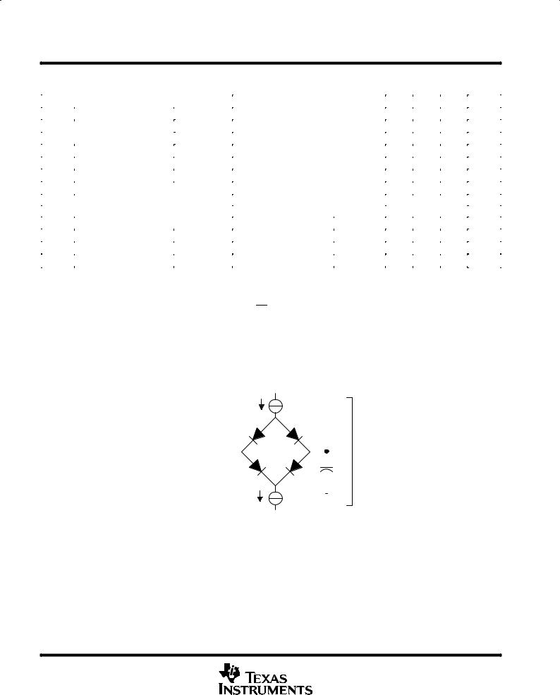
PARAMETER MEASUREMENT INFORMATION
|
|
|
|
IOL |
|
|
|||||
|
Tester Pin |
VLOAD |
|
|
|
|
|
|
|
|
Output |
|
|
|
|
|
|
|
|
|
Under |
||
|
Electronics |
|
|
|
|
|
|
|
|
|
Test |
|
|
|
|
|
|
|
|
|
|
CT |
|
|
|
|
|
|
|
|
|
|
|
||
|
|
|
|
|
|
|
|
|
|
||
|
|
|
|
|
|
|
|
|
|
|
|
|
|
|
|
|
|
|
|
|
|
||
|
|
|
|
IOH |
|
|
|||||
Where: IOL |
= 2 mA (all outputs) |
|
|
|
|
|
|
|
|
|
|
IOH |
= 300 µA (all outputs) |
|
|
||||||||
VLOAD = Selected to emulate 50 Ω termination (typical value = 1.54 V). |
|
|
|||||||||
CT |
= 80-pF typical load-circuit capacitance |
|
|
||||||||
Figure 4. Test Load Circuit
12 |
POST OFFICE BOX 1443 •HOUSTON, TEXAS 77251±1443 |
SMJ320C30
DIGITAL SIGNAL PROCESSOR
SGUS014F ± FEBRUARY 1991 ± REVISED FEBRUARY 1999
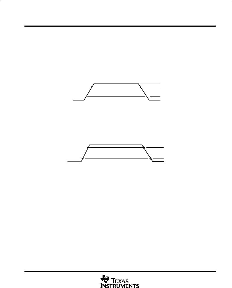
PARAMETER MEASUREMENT INFORMATION
signal transition levels
TTL-level outputs are driven to a minimum logic-high level of 2.4 V and to a maximum logic-low level of 0.6 V. Output transition times are specified as follows:
DFor a high-to-low transition on a TTL-compatible output signal, the level at which the output is said to be no longer high is 2 V and the level at which the output is said to be low is 1 V.
DFor a low-to-high transition, the level at which the output is said to be no longer low is 1 V and the level at which the output is said to be high is 2 V.
2.4 V
2 V
1 V
0.6 V
Figure 5. TTL-Level Outputs
Transition times for TTL-compatible inputs are specified as follows:
DFor a high-to-low transition on an input signal, the level at which the input is said to be no longer high is
2.1V and the level at which the input is said to be low is 0.8 V.
DFor a low-to-high transition on an input signal, the level at which the input is said to be no longer low is
0.8V and the level at which the input is said to be high is 2.1 V.
2.1 V
0.8 V
Figure 6. TTL-Level Inputs
POST OFFICE BOX 1443 •HOUSTON, TEXAS 77251±1443 |
13 |

SMJ320C30
DIGITAL SIGNAL PROCESSOR
SGUS014F ± FEBRUARY 1991 ± REVISED FEBRUARY 1999
PARAMETER MEASUREMENT INFORMATION
timing parameter symbology
Timing parameter symbols used herein were created in accordance with JEDEC Standard 100-A. To shorten the symbols, some of the terminal names and other related terminology have been abbreviated as follows, unless otherwise noted:
A |
A23 ± A0 |
IACK |
IACK |
||||||||||||||||||||||||||||||||
ASYNCH |
Asynchronous reset signals include XF0, XF1, |
|
|
|
|
|
|
|
|
|
|
|
|
|
|
|
|
|
|
|
|
|
|
|
|
|
|
||||||||
|
CLKX0, DX0, FSX0, CLKR0, DR0, FSR0, CLKX1, |
INT |
INT3± |
|
|
|
|
INT0 |
|
|
|
|
|
|
|
|
|
|
|
|
|||||||||||||||
|
DX1, FSX1, CLKR1, DR1, FSR1, TCLK0, and TCLK1 |
|
|
|
|
|
|
|
|
|
|
|
|
|
|
|
|
|
|
|
|
|
|
|
|
|
|
||||||||
CH |
CLKX includes CLKX0 and CLKX1 |
IOS |
|
|
|
|
|
|
|
|
|
|
|
|
|
|
|
|
|
|
|
|
|
||||||||||||
IOSTRB |
|
|
|
|
|
|
|
|
|
|
|
|
|
|
|||||||||||||||||||||
CI |
CLKIN |
(M)S |
|
|
|
|
|
|
|
|
|
|
|
|
|
|
|
and |
|
|
|
||||||||||||||
(M)STRB |
includes |
MSTRB |
STRB |
|
|||||||||||||||||||||||||||||||
|
|
|
|
|
|
|
|
|
|
|
|
|
|
|
|
|
|
|
|
|
|
|
|
|
|||||||||||
CONTROL |
Control signals include |
STRB, |
|
MSTRB, |
and |
IOSTRB |
|
RDY |
RDY |
|
|
|
|
|
|
|
|
|
|
|
|
|
|
||||||||||||
D |
D31 ± D0 |
RESET |
|
|
|
|
|
|
|
|
|
|
|
|
|
|
|||||||||||||||||||
RESET |
|
|
|
|
|
|
|
|
|
||||||||||||||||||||||||||
|
|
|
|
|
|
|
|
|
|
|
|
|
|
|
|
|
|||||||||||||||||||
DR |
Includes DR0, DR1 |
RW |
R / |
W |
|
|
|
|
|
|
|
|
|
|
|
|
|||||||||||||||||||
DX |
Includes DX0, DX1 |
S |
|
|
|
|
|
|
|
|
|
|
|
||||||||||||||||||||||
STRB |
|
|
|
|
|
|
|
|
|
|
|||||||||||||||||||||||||
FS |
FSX/R includes FSX0, FSX1, FSR0, and FSR1 |
SCK |
CLKX/R includes CLKX0, CLKX1, |
||||||||||||||||||||||||||||||||
|
CLKR0, and CLKR1 |
||||||||||||||||||||||||||||||||||
|
|
|
|
|
|
|
|
|
|
|
|||||||||||||||||||||||||
FSR |
Includes FSR0, FSR1 |
TCLK |
TCLK0, TCLK1 |
||||||||||||||||||||||||||||||||
FSX |
Includes FSX0, FSX1 |
(X)A |
Includes A23 ± A0 and XA12 ± XA0 |
||||||||||||||||||||||||||||||||
GPIO |
General-purpose input/output; peripheral pins include |
|
|
|
|
|
|
|
|
|
|
|
|
|
|
|
|
|
|
|
|
|
|
|
|
|
|
||||||||
|
CLKX0/1, CLKR0/1, DX0/1, DR0/1, FSX0/1, FSR0/1, |
(X)D |
Includes D31 ± D0 and XD31 ± XD0 |
||||||||||||||||||||||||||||||||
|
and TCLK0/1 |
|
|
|
|
|
|
|
|
|
|
|
|
|
|
|
|
|
|
|
|
|
|
|
|
|
|
||||||||
H |
Includes H1, H3 |
XF |
XFx includes XF0 and XF1 |
||||||||||||||||||||||||||||||||
H1 |
H1 |
XF0 |
XF0 |
||||||||||||||||||||||||||||||||
H3 |
H3 |
XF1 |
XF1 |
||||||||||||||||||||||||||||||||
HOLD |
|
|
(X)RDY |
Includes |
|
and |
|
|
|
|
|
|
|||||||||||||||||||||||
HOLD |
|
|
RDY |
XRDY |
|
|
|
||||||||||||||||||||||||||||
HOLDA |
|
|
(X)RW |
|
|
|
|
|
|
|
|||||||||||||||||||||||||
HOLDA |
|
(X)R/W |
includes R/W |
and XR/W |
|||||||||||||||||||||||||||||||
14 |
POST OFFICE BOX 1443 •HOUSTON, TEXAS 77251±1443 |
 Loading...