


Texas Instruments SM320C40GFM33, SM320C40GFM40, SM320C40GFM50, SM320C40GFS60, SM320C40HFHM33 Datasheet
...A A E
SGUS017F ± OCTOBER 1993 ± REVISED APRIL 2000
SMJ: QML Processing to MIL±PRF±38535
SM: Standard Processing
TMP: Commercial Level Processing TAB
Operating Temperature Ranges:
±Military (M) ±55°C to 125°C
±Special (S) ±55°C to 100°C
±Commercial (C) ±25°C to 85°C
±Commercial (L) 0°C to 70°C
Highest Performance Floating-Point Digital Signal Processor (DSP)
±'C40-60:
33-ns Instruction Cycle Time:
60 MFLOPS, 30 MIPS, 330 MOPS,
384 MBps
±'C40-50:
40-ns Instruction Cycle Time:
50 MFLOPS, 25 MIPS, 275 MOPS,
320 MBps
±'C40-40:
50-ns Instruction Cycle Time:
40 MFLOPS, 20 MIPS, 220 MOPS,
256 MBps
Six Communications Ports
6-Channel Direct Memory Access (DMA) Coprocessor
Single-Cycle Conversion to and From IEEE-745 Floating-Point Format
Single Cycle 1/x, 1/ x
Source-Code Compatible With SMJ320C30
Validated Ada Compiler
Single-Cycle 40-Bit Floating-Point, 32-Bit Integer Multipliers
12 40-Bit Registers, 8 Auxiliary Registers,
14 Control Registers, and 2 Timers
IEEE Standard 1149.1² Test-Access Port (JTAG)
Two Identical External Data and Address Buses Supporting Shared Memory Systems and High Data-Rate, Single-Cycle Transfers:
±High Port-Data Rate of 100 MBytes/s (Each Bus)
±16G-Byte Continuous Program/Data/Peripheral Address Space
±Memory-Access Request for Fast, Intelligent Bus Arbitration
±Separate Address-, Data-, and Control-Enable Pins
±Four Sets of Memory-Control Signals Support Different Speed Memories in Hardware
Packaging:
±325-Pin Ceramic Grid Array (GF Suffix)
±352-Lead Ceramic Quad Flatpack (HFH Suffix)
±324-Pad JEDEC-Standard TAB Frame
Fabricated Using 0.72- m Enhanced Performance Implanted CMOS (EPIC ) Technology by Texas Instruments (TI )
Separate Internal Program, Data, and DMA Coprocessor Buses for Support of Massive Concurrent Input/Output (I/O) of Program and Data Throughput, Maximizing Sustained Central Processing Unit (CPU) Performance
On-Chip Program Cache and Dual-Access/Single-Cycle RAM for Increased Memory-Access Performance
±512-Byte Instruction Cache
±8K Bytes of Single-Cycle Dual-Access Program or Data RAM
±ROM-Based Bootloader Supports Program Bootup Using 8-, 16-, or 32-Bit Memories Over Any One of the Communications Ports
Please be aware that an important notice concerning availability, standard warranty, and use in critical applications of Texas Instruments semiconductor products and disclaimers thereto appears at the end of this data sheet.
² IEEE Standard 1149.1-1990, IEEE Standard Test-Access Port and Boundary-Scan Architecture. EPIC and TI are trademarks of Texas Instruments Incorporated.
A A |
#& ')% +#'& #* |
,)) &+ |
* |
' |
(, $# +#'& + |
|||
)' , +* |
'& ')% |
+' |
*( # # +#'&* |
( ) |
+" |
+ )%* |
' |
. * &*+),% &+* |
*+ & ) |
- )) &+/ |
)' , +#'& ()' **#&! |
' * &'+ |
& ** )#$/ #& $, |
||||
+ *+#&! ' |
$$ ( ) % + )* |
|
|
|
|
|
||
POST OFFICE BOX 1443 •HOUSTON, TEXAS 77251±1443
Copyright 2000, Texas Instruments Incorporated
& ()' , +* '%($# &+ +' 0 0 8 |
$$ |
( ) % + )* |
) + *+ |
||
,&$ ** '+" )-#* |
&'+ & |
$$ '+" ) |
()' , +* |
()' , +#'& |
|
()' **#&! ' * |
&'+ & ** )#$/ |
#& $, |
+ *+#&! ' $$ |
( ) % + )* |
|
|
|
|
|
|
1 |

SMJ320C40 TMP320C40
DIGITAL SIGNAL PROCESSORS
SGUS017F ± OCTOBER 1993 ± REVISED APRIL 2000
description
352-LEAD HFH QUAD FLATPACK PACKAGE |
|
|
325-PIN GF GRID ARRAY PACKAGE |
|
|
|
|||||||||||||||||||||||
(TOP VIEW)² |
|
|
|
|
|
|
|
(BOTTOM VIEW)² |
|
|
|
|
|
|
|
|
|
||||||||||||
352 |
265 |
|
|
|
|
|
|
|
|
|
|
|
|
|
|
|
|
|
|
|
|
|
|
|
|
|
|
|
|
|
|
AR |
|
|
|
|
|
|
|
|
|
|
|
|
|
|
|
|
|
|
|
|
|
|
|
|
|
|
|
|
|
AP |
|
|
|
|
|
|
|
|
|
|
|
|
|
|
|
|
|
|
|
|
|
|
|
|
|
|
|
|
|
AN |
|
|
|
|
|
|
|
|
|
|
|
|
|
|
|
|
|
|
|
|
|
|
|
|
|
|
|
|
|
AM |
|
|
|
|
|
|
|
|
|
|
|
|
|
|
|
|
|
|
|
|
|
|
|
|
|
|
|
|
|
AL |
|
|
|
|
|
|
|
|
|
|
|
|
|
|
|
|
|
|
|
|
|
|
|
|
|
|
|
1 |
264 |
AK |
|
|
|
|
|
|
|
|
|
|
|
|
|
|
|
|
|
|
|
|
|
|
|
|
|
|
|
AJ |
|
|
|
|
|
|
|
|
|
|
|
|
|
|
|
|
|
|
|
|
|
|
|
|
|
|
|
||
|
|
|
|
|
|
|
|
|
|
|
|
|
|
|
|
|
|
|
|
|
|
|
|
|
|
|
|
|
|
|
|
AH |
|
|
|
|
|
|
|
|
|
|
|
|
|
|
|
|
|
|
|
|
|
|
|
|
|
|
|
|
|
AG |
|
|
|
|
|
|
|
|
|
|
|
|
|
|
|
|
|
|
|
|
|
|
|
|
|
|
|
|
|
AF |
|
|
|
|
|
|
|
|
|
|
|
|
|
|
|
|
|
|
|
|
|
|
|
|
|
|
|
|
|
AE |
|
|
|
|
|
|
|
|
|
|
|
|
|
|
|
|
|
|
|
|
|
|
|
|
|
|
|
|
|
AD |
|
|
|
|
|
|
|
|
|
|
|
|
|
|
|
|
|
|
|
|
|
|
|
|
|
|
|
|
|
AC |
|
|
|
|
|
|
|
|
|
|
|
|
|
|
|
|
|
|
|
|
|
|
|
|
|
|
|
|
|
AB |
|
|
|
|
|
|
|
|
|
|
|
|
|
|
|
|
|
|
|
|
|
|
|
|
|
|
|
|
|
AA |
|
|
|
|
|
|
|
|
|
|
|
|
|
|
|
|
|
|
|
|
|
|
|
|
|
|
|
|
|
Y |
|
|
|
|
|
|
|
|
|
|
|
|
|
|
|
|
|
|
|
|
|
|
|
|
|
|
|
|
|
W |
|
|
|
|
|
|
|
|
|
|
|
|
|
|
|
|
|
|
|
|
|
|
|
|
|
|
|
|
|
V |
|
|
|
|
|
|
|
|
|
|
|
|
|
|
|
|
|
|
|
|
|
|
|
|
|
|
|
|
|
U |
|
|
|
|
|
|
|
|
|
|
|
|
|
|
|
|
|
|
|
|
|
|
|
|
|
|
|
|
|
T |
|
|
|
|
|
|
|
|
|
|
|
|
|
|
|
|
|
|
|
|
|
|
|
|
|
|
|
|
|
R |
|
|
|
|
|
|
|
|
|
|
|
|
|
|
|
|
|
|
|
|
|
|
|
|
|
|
|
|
|
P |
|
|
|
|
|
|
|
|
|
|
|
|
|
|
|
|
|
|
|
|
|
|
|
|
|
|
|
|
|
N |
|
|
|
|
|
|
|
|
|
|
|
|
|
|
|
|
|
|
|
|
|
|
|
|
|
|
|
|
|
M |
|
|
|
|
|
|
|
|
|
|
|
|
|
|
|
|
|
|
|
|
|
|
|
|
|
|
|
|
|
L |
|
|
|
|
|
|
|
|
|
|
|
|
|
|
|
|
|
|
|
|
|
|
|
|
|
|
|
|
|
K |
|
|
|
|
|
|
|
|
|
|
|
|
|
|
|
|
|
|
|
|
|
|
|
|
|
|
|
|
|
J |
|
|
|
|
|
|
|
|
|
|
|
|
|
|
|
|
|
|
|
|
|
|
|
|
|
|
|
|
|
H |
|
|
|
|
|
|
|
|
|
|
|
|
|
|
|
|
|
|
|
|
|
|
|
|
|
|
|
|
|
G |
|
|
|
|
|
|
|
|
|
|
|
|
|
|
|
|
|
|
|
|
|
|
|
|
|
|
|
|
|
F |
|
|
|
|
|
|
|
|
|
|
|
|
|
|
|
|
|
|
|
|
|
|
|
|
|
|
|
|
|
E |
|
|
|
|
|
|
|
|
|
|
|
|
|
|
|
|
|
|
|
|
|
|
|
|
|
|
|
|
|
D |
|
|
|
|
|
|
|
|
|
|
|
|
|
|
|
|
|
|
|
|
|
|
|
|
|
|
|
|
|
C |
|
|
|
|
|
|
|
|
|
|
|
|
|
|
|
|
|
|
|
|
|
|
|
|
|
|
|
|
|
B |
|
|
|
|
|
|
|
|
|
|
|
|
|
|
|
|
|
|
|
|
|
|
|
|
|
|
|
|
|
A |
|
|
|
|
|
|
|
|
|
|
|
|
|
|
|
|
|
|
|
|
|
|
|
|
|
|
|
88 |
177 |
|
2 |
4 |
6 |
8 |
10 |
12 |
14 |
16 |
18 |
20 |
22 |
24 |
26 |
28 |
30 32 |
34 |
|||||||||||
|
|
1 |
3 |
5 |
7 |
9 |
11 |
13 |
15 |
17 |
19 |
21 |
23 |
25 |
27 |
29 31 |
33 |
35 |
|||||||||||
|
|
Pin A1 |
|
|
|
|
|
|
|
|
|
|
|
|
|
|
|
|
|
|
|
|
|
|
|
|
|
|
|
89 |
176 |
|
|
|
|
|
|
|
|
|
|
|
|
|
|
|
|
|
|
|
|
|
|
|
|
|
|
|
|
TAB 325-LEAD OLB/ILB
TAPE AUTOMATED BONDING (TAB) PACKAGE
(TOP VIEW)²
1 

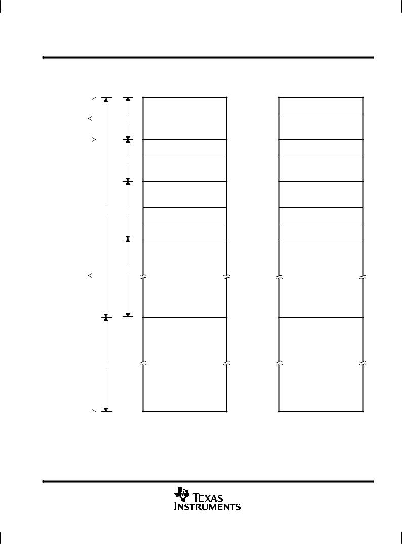
² See the pin assignments tables and the signal description table for location and description of all pins.
2 |
POST OFFICE BOX 1443 •HOUSTON, TEXAS 77251±1443 |

SMJ320C40 TMP320C40
DIGITAL SIGNAL PROCESSORS
SGUS017F ± OCTOBER 1993 ± REVISED APRIL 2000
description (continued)
The '320C40 digital signal processors (DSPs) are 32-bit, floating-point processors manufactured in 0.72- m, double-level metal CMOS technology. The '320C40 is a part of the fourth-generation DSPs from Texas Instruments and is designed primarily for parallel processing.
operation
The '320C40 has six on-chip communication ports for processor-to-processor communication with no external hardware and simple communication software. This allows connectivity to other 'C4x processors with no external-glue logic. The communication ports remove input/output bottlenecks, and the independent smart DMA coprocessor is able to handle the CPU input/output burden.
central processing unit
The '320C40 CPU is configured for high-speed internal parallelism for the highest sustained performance. The key features of the CPU are:
Eight operations/cycle:
±40/32-bit floating-point/integer multiply
±40/32-bit floating-point/integer arithmetic logic unit (ALU) operation
±Two data accesses
±Two address-register updates
IEEE floating-point conversion
Divide and square-root support
'C3x assembly language compatibility
Byte and halfword accessibility
DMA coprocessor
The DMA coprocessor allows concurrent I/O and CPU processing for the highest sustained CPU performance. The key features of the DMA processor are:
Link pointers that allow DMA channels to autoinitialize without CPU intervention
Parallel CPU operation and DMA transfers
Six DMA channels that support memory-to-memory data transfers
Split-mode operation doubles the available DMA channels to 12 when data transfers to and from a communication port are required.
communication ports
The '320C40 is the first DSP with on-chip communication ports for processor-to-processor communication with no external hardware and simple communication software. The features of the communication ports are:
Direct interprocessor communication and processor I/O
Six communication ports for direct interprocessor communication and processor I/O
20M-byte/s bidirectional interface on each communication port for high-speed multiprocessor interface
Separate 8-word-deep input and output FIFO buffers for processor-to-processor communication and I/O
Automatic arbitration and handshaking for direct processor-to-processor connection
POST OFFICE BOX 1443 •HOUSTON, TEXAS 77251±1443 |
3 |

SMJ320C40 TMP320C40
DIGITAL SIGNAL PROCESSORS
SGUS017F ± OCTOBER 1993 ± REVISED APRIL 2000
communication-port software reset ('C40 silicon revision ≥ 5.0)
The input and output FIFO levels for a communication port can be flushed by writing at least two back-to-back values to its communication-port software-reset address as specified in Table 1. This feature is not present in 'C40 silicon revision < 5.0. This software reset flushes any word or byte already present in the FIFOs but it does not affect the status of the communication-port pins. Figure 1 shows an example of communication-port-software reset.
Table 1. Communication-Port Software-Reset Address
0 |
0x0100043 |
|
|
1 |
0x0100053 |
|
|
2 |
0x0100063 |
|
|
3 |
0x0100073 |
|
|
4 |
0x0100083 |
|
|
5 |
0x0100093 |
;±±±±±±±±±±±±±±±±±±±±±±±±±±±±±±±±±±±±±±±±±±±±±-±±±;
;RESET1:Flush's FIFO data for communication port 1;
;±±±±±±±±±±±±±±±±±±±±±±±±±±±±±±±±±±±±±±±±±±±±±-±±±;
RESET1 push |
AR0 |
; |
Save registers |
push |
R0 |
; |
|
push |
RC |
; |
|
ldhi |
010h,AR0 |
; Set AR0 to base address of COM 1 |
|
or |
050h,AR0 |
; |
|
flush: rpts |
1 |
; Flush FIFO data with back-to-back write |
|
sti |
R0,*+AR0(3) |
; |
|
rpts |
10 |
; |
Wait |
nop |
|
; |
|
ldi |
*+AR0(0),R0 |
; Check for new data from other port |
|
and |
01FE0h,R0 |
; |
|
bnz |
flush |
; |
|
pop |
RC |
; |
Restore registers |
pop |
R0 |
; |
|
pop |
AR0 |
; |
|
rets |
|
; |
Return |
Figure 1. Example of Communication-Port-Software Reset
4 |
POST OFFICE BOX 1443 •HOUSTON, TEXAS 77251±1443 |

SMJ320C40 TMP320C40
DIGITAL SIGNAL PROCESSORS
SGUS017F ± OCTOBER 1993 ± REVISED APRIL 2000
NMI with bus-grant feature ('C40 silicon revision ≥ 5.0)
The '320C40 devices have a software-configurable feature that forces the internal-peripheral bus to ready when the NMI signal is asserted. This feature is not present in 'C40 silicon revision < 5.0. The NMI bus-grant feature is enabled when bits 19±18 of the status register (ST) are set to 10b. When enabled, a peripheral bus-grant signal is generated on the falling edge of NMI. When NMI is asserted and this feature is not enabled, the CPU stalls on access to the peripheral bus if it is not ready. A stall condition occurs when writing to a full FIFO or reading an empty FIFO. This feature is useful in correcting communication-port errors when used in conjunction with the communication-port software-reset feature.
IDLE2 clock-stop power-down mode ('C40 silicon revision ≥ 5.0)
The '320C40 has a clock-stop mode or power-down mode (IDLE2) to achieve extremely low power consumption. When an IDLE2 instruction is executed, the clocks are halted with H1 being held high. To exit IDLE2, assert one of the IIOF3±IIOF0 pins configured as an external interrupt instead of a general-purpose I/O. A macro showing how to generate the IDLE2 opcode is given in Figure 2. During this power-down mode:
No instructions are executed
The CPU, peripherals, and internal memory retain their previous state.
The external-bus outputs are idle. The address lines remain in their previous state, the data lines are in the high-impedance state, and the output-control signals are inactive.
;±±±±±±±±±±±±±±±±±±±±±±±±±±±±±±±±±±±±±±±±±±±±-±-±;
; IDLE2: Macro to generate idle2 opcode |
; |
; ±±±±±±±±±±±±±±±±±±±±±±±±±±±±±±±±±±±±±±±±±±±±±-±±;
IDLE2 .macro
.word 06000001h
.endm
Figure 2. Example of Software Subroutine Using IDLE2
IDLE2 is exited when one of the five external interrupts (NMI and IIOF3±IIOF0) is asserted low for at least four input clocks (two H1 cycles). The clocks then start after a delay of two input clocks (one H1 cycle). The clocks can start in the opposite phase; that is, H1 can be high when H3 was high before the clocks were stopped. However, the H1 and H3 clocks remain 180° out of phase with each other.
During IDLE2 operation, an external interrupt can be recognized and serviced by the CPU if it is enabled before entering IDLE2 and asserted for at least two H1 cycles. For the processor to recognize only one interrupt, the interrupt pin must be configured for edge-trigger mode or asserted less than three cycles in level-trigger mode. Any external interrupt pin can wake up the device from IDLE2, but for the CPU to recognize that interrupt, it must also be enabled. If an interrupt is recognized and executed by the CPU, the instruction following the IDLE2 instruction is not executed until after execution of a return opcode.
When the device is in emulation mode, the CPU executes an IDLE2 instruction as if it were an IDLE instruction. The clocks continue to run for correct operation of the emulator.
POST OFFICE BOX 1443 •HOUSTON, TEXAS 77251±1443 |
5 |

SMJ320C40 TMP320C40
DIGITAL SIGNAL PROCESSORS
SGUS017F ± OCTOBER 1993 ± REVISED APRIL 2000
development tools
The 'C40 is supported by a host of parallel-processing development tools for developing and simulating code easily and for debugging parallel-processing systems. The code generation tools include:
An ANSI C compiler optimized with a runtime support library that supports use of communication ports and DMA.
Third-party support for C, C++, and Ada compilers
Several operating systems available for parallel-processing support, as well as DMA and communication port drivers
An assembler and linker with support for mapping program and data to parallel processors
The simulation tools include:
Parallel DSP system-level simulation with LAI hardware verification (HV) model and full function (FF) model
TI software simulator with high-level language debugger interface for simulating a single processor
The hardware development and verification tools include:
Parallel processor in-circuit emulator and high-level language debugger: XDS510
Parallel processor development system (PPDS) with four '320C40s, local and global memory, and communication port connections
XDS510 is a trademark of Texas Instruments Incorporated.
6 |
POST OFFICE BOX 1443 •HOUSTON, TEXAS 77251±1443 |

SMJ320C40 TMP320C40 DIGITAL SIGNAL PROCESSORS
SGUS017F ± OCTOBER 1993 ± REVISED APRIL 2000
block diagram
D31±D0

A30±A0 DE
DE  AE
AE 
STAT3±STAT0 LOCK
LOCK STRB0,STRB1
 R/W0,RW1
 PAGE0,PAGE1
 RDY0,RDY1
  CE0,CE1
X1
X2/CLKIN
ROMEN
RESET
RESETLOC0,
RESETLOC1
NMI
IIOF3±IIOF0
IACK
H1
H3
CVSS
DVDD
DVSS
IVSS
LADVDD
LDDVDD
VDDL
VSSL
SUBS
|
Cache |
RAM Block 0 |
RAM Block 1 |
ROM Block |
|||
(512 Bytes) |
|
(4K Bytes) |
(4K Bytes) |
(Reserved) |
|||
32 |
32 |
32 |
32 |
32 |
32 |
32 |
32 |
PDATA Bus
PADDR Bus
DDATA Bus
M
U DADDR 1 Bus
X
DADDR 2 Bus
DMADATA Bus
DMAADDR Bus
32 |
32 |
32 |
32 |
32 |
IR
PC |
MUX |
|
|
|
|
|
CPU1 |
|
|
|
|
|
|
CPU2 |
|
|
C |
|
|
|
REG11 |
|
|
|
|
|
|
|
|
|
o |
C |
R |
R |
REG2 |
|
|
n |
|
|
||||
P |
E |
E |
|
|
||
t |
|
|
|
|||
U |
G |
G |
|
|
|
|
r |
|
|
|
|||
1 |
1 |
2 |
|
|
|
|
o |
|
|
|
|||
|
|
40 |
40 |
40 |
40 |
|
l |
|
|
||||
|
|
|
|
32-Bit Barrel |
||
l |
|
|
Multiplier |
|||
e |
|
|
Shifter |
|
||
|
|
|
|
|
||
r |
|
|
|
|
ALU |
|
40 |
40 |
|
40 |
|
|
|
|||
|
|
40 |
||
40 |
Extended |
|||
|
||||
Precision |
|
|||
|
40 |
|||
32 |
Registers |
|||
|
(R0±R11) |
|
||
|
DISP, IR0, IR1 |
|
||
|
ARAU0 |
ARAU1 |
||
|
|
BK |
|
|
Continued on next page
32 |
|
32 |
|
|
|
||
32 |
Auxiliary |
32 |
|
32 |
Registers |
32 |
|
32 |
(AR0±AR7) |
||
|
|||
|
|
||
32 |
|
32 |
|
|
Other |
||
32 |
|
||
Registers |
|
||
|
(14) |
|
POST OFFICE BOX 1443 •HOUSTON, TEXAS 77251±1443 |
7 |

SMJ320C40 TMP320C40
DIGITAL SIGNAL PROCESSORS
SGUS017F ± OCTOBER 1993 ± REVISED APRIL 2000
block diagram (continued)
page |
PDATA Bus |
|
|
|
|
|
|
|
|
LD31±LD0 |
|
|
|
|
|
|
|
|
|
||
PADDR Bus |
|
|
|
|
|
|
|
|
LA30±LA0 |
|
previous |
|
|
|
|
|
|
|
|
LDE |
|
|
|
|
|
|
|
|
|
|
||
DDATA Bus |
|
|
|
|
|
|
|
|
LAE |
|
|
|
|
|
|
|
|
|
LSTAT3±LSTAT0 |
||
|
|
|
|
|
|
M |
|
|
||
|
|
|
|
|
|
|
|
LLOCK |
||
DADDR 1 Bus |
|
|
|
|
|
U |
|
|
||
from |
|
|
|
|
|
|
|
|||
|
|
|
|
|
|
X |
|
|
LSTRB0±LSTRB1 |
|
DADDR 2 Bus |
|
|
|
|
|
|
|
|
LR/W0±LR/W1 |
|
Continued |
|
|
|
|
|
|
|
|
||
|
|
|
|
|
|
|
|
LPAGE0±LPAGE1 |
||
|
|
|
|
|
|
|
|
|
||
DMADATA Bus |
|
|
|
|
|
|
|
|
LRDY0±LRDY1 |
|
|
|
|
|
|
|
|
|
|
LCE0, LCE1 |
|
DMAADDR Bus |
|
|
|
|
|
|
|
|
|
|
|
|
|
|
|
|
|
|
|
|
|
|
32 |
32 |
|
MUX |
|
|
|
|
|
|
|
|
|
32 |
|
|
|
|
|
||
|
|
|
|
|
COM Port 0 |
|
|
|
||
|
|
|
|
|
|
|
|
|
||
|
|
|
|
|
32 |
Input |
|
CREQ0 |
|
|
|
|
|
32 |
|
|
FIFO |
|
CACK0 |
|
|
|
DMA Coprocessor |
|
32 |
Output |
PAU |
CSTRB0 |
|
Ports |
||
|
|
|
|
CRDY0 |
|
|||||
|
DMA Channel 0 |
|
|
|
FIFO |
|
|
|||
|
|
|
32 |
|
C0D7±C0D0 |
|||||
|
|
|
Port Control Registers |
Communication |
||||||
|
DMA Channel 1 |
|
|
|
|
|
||||
|
DMA Channel 2 |
|
P |
|
|
|
|
|
||
|
DMA Channel 3 |
32 |
e |
|
|
|
|
|
||
|
r |
|
|
|
|
|
||||
|
|
|
|
|
|
|
|
|
||
|
DMA Channel 4 |
P |
i |
32 |
COM Port 5 |
|
|
|||
|
DMA Channel 5 |
e |
p |
|
|
|
||||
|
r |
h |
32 |
Input |
|
CREQ5 |
|
|||
|
|
|
|
|
||||||
|
|
|
i |
e |
|
CACK5 |
|
Six |
||
|
|
|
|
FIFO |
|
|
||||
|
|
|
p |
r |
32 |
|
PAU |
CSTRB5 |
|
|
|
Six DMA Channels |
h |
a |
Output |
|
|
||||
|
|
|
CRDY5 |
|
|
|||||
|
|
|
e |
l |
32 |
FIFO |
|
C5D7±C5D0 |
||
|
|
|
r |
A |
Port Control Registers |
|||||
|
|
|
a |
|
|
|
|
|||
|
|
|
l |
d |
32 |
|
|
|
|
|
|
|
|
|
d |
|
Timer 0 |
|
|
|
|
|
|
|
D |
r |
|
|
|
|
|
|
|
|
|
|
|
|
|
|
|
||
|
|
|
a |
e |
32 |
Global Control Register |
|
|
|
|
|
|
|
t |
s |
|
Time Period Register |
|
TCLK0 |
||
|
|
|
a |
s |
|
|
|
|
||
|
|
|
|
Timer Counter Register |
|
|
|
|||
|
|
|
|
|
32 |
|
|
|
||
|
|
|
B |
B |
|
|
|
|
|
|
|
|
|
|
|
|
|
|
|
||
|
|
|
u |
u |
|
Timer 1 |
|
|
|
|
|
|
|
s |
s |
32 |
Global Control Register |
|
|
|
|
|
|
|
|
|
|
|
|
|||
|
Time Period Register |
TCLK1 |
|
Timer Counter Register |
|
32 |
Port Control |
|
|
Global |
|
32 |
Local |
|
|
|
8 |
POST OFFICE BOX 1443 •HOUSTON, TEXAS 77251±1443 |
SMJ320C40 TMP320C40
DIGITAL SIGNAL PROCESSORS
SGUS017F ± OCTOBER 1993 ± REVISED APRIL 2000
memory map
Figure 3 shows the memory map for the '320C40. See the TMS320C4x User's Guide (literature number SPRU063) for a detailed description of this memory mapping.
Structure |
|
Accessible Local Bus |
|
Depends |
1M |
||
(External) |
|||
Upon |
|||
|
|
||
ROMEN Bit |
|
|
Peripherals (Internal)
1M |
Reserved
|
|
|
Reserved |
|
2G |
1M |
1K RAM BLK 0 (Internal) |
|
|
||
|
|
|
|
|
|
|
1K RAM BLK 1 (Internal) |
Structure |
|
2G±3M |
|
|
|
Local Bus |
|
Identical |
|
|
|
|
|
|
(External) |
|
2G |
|
Global Bus (External) |
|
|
|
(a) Internal ROM Disabled
(ROMEN = 0)
Microprocessor Mode
000000000h
000000FFFh
000001000h
0000FFFFFh
000100000h
0001000FFh
000100100h
0001FFFFFh
000200000h
0002FF7FFh
0002FF800h
0002FFBFFh
0002FFC00h
0002FFFFFh
000300000h
07FFFFFFFh
080000000h
0FFFFFFFFh
Boot-Loader ROM
(Internal)
Reserved
Peripherals (Internal)
Reserved
Reserved
1K RAM BLK 0 (Internal)
1K RAM BLK 1 (Internal)
Local Bus
(External)
Global Bus (External)
(b) Internal ROM Enabled
(ROMEN = 1)
Microcomputer Mode
Figure 3. Memory Map for '320C40
POST OFFICE BOX 1443 •HOUSTON, TEXAS 77251±1443 |
9 |

SMJ320C40 TMP320C40
DIGITAL SIGNAL PROCESSORS
SGUS017F ± OCTOBER 1993 ± REVISED APRIL 2000
signal descriptions
This section gives signal descriptions for the SMJ320C40 device. The SMJ320C40 signal descriptions table lists each signal, the number of pins, operating mode(s) (that is, input, output, or high-impedance state as indicated by I, O, or Z, respectively), and function. All pins labeled NC are not to be connected by the user. A line over a signal name (for example, RESET) indicates that the signal is active low (true at a logic-0 level). The signals are grouped according to functions.
|
|
|
|
|
|
|
|
|
|
|
|
|
|
|
|
|
|
|
SMJ320C40 Signal Descriptions |
|||||||||||||||
|
|
|
|
|
|
|
|
|
|
|
|
|
|
|
|
|
|
|
|
|
|
|
|
|
|
|
|
|
|
|
|
|
|
|
|
|
|
|
|
|
|
|
|
|
|
|
|
|
|
SIGNAL |
|
|
|
|
|
|
|
|
|
|
|
|
|
|
|
|
|
|
|
|
|
|
|
|
|
|
|
|
|
|
|
NAME |
NO. OF |
TYPE² |
|
|
|
|
|
|
|
|
|
|
|
|
DESCRIPTION |
|||||||
|
|
|
|
|
|
|
|
|
|
|
|
PINS |
|
|
|
|
|
|
|
|
|
|
|
|
|
|
|
|
|
|
||||
|
|
|
|
|
|
|
|
|
|
|
|
|
|
|
|
|
|
|
|
|
|
|
|
|
|
|
|
|
|
|
|
|
|
|
|
|
|
|
|
|
|
|
|
|
|
|
|
|
|
|
|
|
|
|
|
|
|
|
|
|
|
|
|
|
|
|
|
|
|
|
|
|
|
|
|
|
|
|
|
|
|
|
|
|
|
|
|
GLOBAL BUS EXTERNAL INTERFACE (80 PINS) |
||||||||||||||||
|
|
|
|
|
|
|
|
|
|
|
|
|
|
|
|
|
|
|
|
|
|
|
|
|
|
|
|
|
|
|
|
|
|
|
|
D31±D0 |
32 |
I/O/Z |
|
32-bit data port of the global bus external interface |
|||||||||||||||||||||||||||||
|
|
|
|
|
|
|
|
|
|
|
|
|
|
|
|
|
|
|
|
|
|
|
|
|
|
|
|
|
|
|
|
|
|
|
|
|
|
|
|
|
|
|
|
|
|
|
|
|
|
|
1 |
I |
|
Data-bus-enable signal for the global bus external interface |
|||||||||||||||
|
DE |
|
|
|
|
|
|
|
|
|
|
|
|
|
||||||||||||||||||||
|
|
|
|
|
|
|
|
|
|
|
|
|
|
|
|
|
|
|
|
|
|
|
|
|
|
|
|
|
|
|
|
|
|
|
|
A30±A0 |
31 |
O/Z |
|
31-bit address port of the global bus external interface |
|||||||||||||||||||||||||||||
|
|
|
|
|
|
|
|
|
|
|
|
|
|
|
|
|
|
|
|
|
|
|
|
|
|
|
|
|
|
|
|
|
||
|
|
|
|
|
|
|
|
|
|
|
|
|
|
|
|
1 |
I |
|
Address-bus-enable signal for the global bus external interface |
|||||||||||||||
|
AE |
|
|
|
|
|
|
|
|
|
|
|
|
|
||||||||||||||||||||
|
|
|
|
|
|
|
|
|
|
|
|
|
|
|
|
|
|
|
|
|
|
|
|
|
|
|
|
|
|
|
|
|
||
|
STAT3±STAT0 |
4 |
O |
|
Status signals for the global bus external interface |
|||||||||||||||||||||||||||||
|
|
|
|
|
|
|
|
|
|
|
|
|
|
|
|
|
|
|
|
|
|
|
|
|
|
|
|
|
|
|
|
|||
|
|
|
|
|
|
|
|
|
|
|
|
|
|
|
|
1 |
O |
|
Lock signal for the global bus external interface |
|||||||||||||||
|
LOCK |
|
|
|
|
|
||||||||||||||||||||||||||||
|
|
|
|
|
|
|
|
|
|
|
|
|
|
|
|
|
|
|
|
|
|
|
|
|
|
|
|
|
|
|
|
|||
|
|
|
|
|
|
|
|
|
|
|
|
|
³ |
|
1 |
O/Z |
|
Access strobe 0 for the global bus external interface |
||||||||||||||||
|
STRB0 |
|
||||||||||||||||||||||||||||||||
|
|
|
|
|
|
|
|
|
|
|
|
|
|
|
|
|
|
|
|
|
|
|
|
|
|
|
|
|
|
|||||
|
|
|
|
|
|
|
³ |
|
|
1 |
O/Z |
|
Read/write signal for |
|
|
|
|
|
|
accesses |
||||||||||||||
|
R/W0 |
|
STRB0 |
|||||||||||||||||||||||||||||||
|
|
|
|
|
|
|
|
|
|
|
|
|
|
|
|
|
|
|
|
|
|
|
|
|
|
|
||||||||
|
PAGE0³ |
|
|
|
|
|
|
|
|
|
|
|
|
|
|
|
||||||||||||||||||
|
1 |
O/Z |
|
Page signal for |
STRB0 |
accesses |
||||||||||||||||||||||||||||
|
|
|
|
|
|
|
|
|
|
|
³ |
|
|
1 |
I |
|
Ready signal for |
|
|
|
|
|
accesses |
|||||||||||
|
RDY0 |
|
STRB0 |
|||||||||||||||||||||||||||||||
|
|
|
|
|
|
|
|
|
|
|
|
|
|
|
|
|
|
|
|
|
|
|||||||||||||
|
|
|
|
|
|
|
|
³ |
|
|
|
|
1 |
I |
|
Control enable for the |
|
|
|
|
|
|
|
|
|
|
signals |
|||||||
|
CE0 |
|
STRB0, |
|
PAGE0, and R/W0 |
|
||||||||||||||||||||||||||||
|
|
|
|
|
|
|
|
|
|
|
|
|
|
|
|
|
|
|
||||||||||||||||
|
|
|
|
|
|
|
|
|
|
|
|
|
³ |
|
1 |
O/Z |
|
Access strobe 1 for the global bus external interface |
||||||||||||||||
|
STRB1 |
|
||||||||||||||||||||||||||||||||
|
|
|
|
|
|
|
³ |
|
|
1 |
O/Z |
|
Read/write signal for |
|
|
|
|
|
|
accesses |
||||||||||||||
|
R/W1 |
|
STRB1 |
|||||||||||||||||||||||||||||||
|
|
|
|
|
|
|
|
|
|
|
|
|
|
|
|
|
|
|||||||||||||||||
|
PAGE1³ |
|
|
|
|
|
|
|
|
|
|
|||||||||||||||||||||||
|
1 |
O/Z |
|
Page signal for |
STRB1 |
accesses |
||||||||||||||||||||||||||||
|
|
|
|
|
|
|
|
|
|
|
³ |
|
|
1 |
I |
|
Ready signal for |
|
|
|
|
|
accesses |
|||||||||||
|
RDY1 |
|
STRB1 |
|||||||||||||||||||||||||||||||
|
|
|
|
|
|
|
|
|
|
|
|
|
|
|
|
|
|
|
||||||||||||||||
|
|
|
|
|
|
|
|
³ |
|
|
|
|
1 |
I |
|
Control enable for the |
|
|
|
|
|
|
|
|
|
|
signals |
|||||||
|
CE1 |
|
STRB1, |
|
PAGE1, and R/W1 |
|
||||||||||||||||||||||||||||
|
|
|
|
|
|
|
|
|
|
|
|
|
|
|
|
|
|
|
|
|
|
|
|
|
|
|
|
|
|
|
|
|
|
|
|
|
|
|
|
|
|
|
|
|
|
|
|
|
|
|
|
|
LOCAL BUS EXTERNAL INTERFACE (80 PINS) |
||||||||||||||||
|
|
|
|
|
|
|
|
|
|
|
|
|
|
|
|
|
|
|||||||||||||||||
|
LD31±LD0 |
32 |
I/O/Z |
|
32-bit data port of the local bus external interface |
|||||||||||||||||||||||||||||
|
|
|
|
|
|
|
|
|
|
|
|
|
|
|
|
|
|
|||||||||||||||||
|
|
|
|
|
|
|
|
|
|
|
|
|
|
|
|
1 |
I |
|
Data-bus-enable signal for the local bus external interface |
|||||||||||||||
|
LDE |
|
|
|
|
|
|
|||||||||||||||||||||||||||
|
|
|
|
|
|
|
|
|
|
|
|
|
|
|
|
|
|
|||||||||||||||||
|
LA30±LA0 |
31 |
O/Z |
|
31-bit address port of the local bus external interface |
|||||||||||||||||||||||||||||
|
|
|
|
|
|
|
|
|
|
|
|
|
|
|
|
|
||||||||||||||||||
|
|
|
|
|
|
|
|
|
|
|
|
|
|
|
|
1 |
I |
|
Address-bus-enable signal for the local bus external interface |
|||||||||||||||
|
LAE |
|
|
|
|
|
|
|||||||||||||||||||||||||||
|
LSTAT3±LSTAT0 |
4 |
O |
|
Status signals for the local bus external interface |
|||||||||||||||||||||||||||||
|
|
|
|
|
|
|
|
|
|
|
|
|
|
|
|
|||||||||||||||||||
|
|
|
|
|
|
|
|
|
|
|
|
|
|
|
|
1 |
O |
|
Lock signal for the local bus external interface |
|||||||||||||||
|
LLOCK |
|
|
|
||||||||||||||||||||||||||||||
|
|
|
|
|
|
|
|
|
|
|
|
|
|
|
³ |
1 |
O/Z |
|
Access strobe 0 for the local bus external interface |
|||||||||||||||
|
LSTRB0 |
|
||||||||||||||||||||||||||||||||
|
|
|
|
|
|
|
|
|
|
|
|
|
||||||||||||||||||||||
|
|
|
|
|
|
|
|
|
|
|
|
|
|
|
|
1 |
O/Z |
|
Read/write signal for |
|
|
|
|
|
|
|
accesses |
|||||||
|
LR/W0 |
|
|
|
LSTRB0 |
|||||||||||||||||||||||||||||
|
|
|
|
|
|
|
|
|
|
|
|
|||||||||||||||||||||||
|
|
|
|
|
|
|
|
|
|
|
||||||||||||||||||||||||
|
LPAGE0 |
1 |
O/Z |
|
Page signal for |
LSTRB0 |
accesses |
|||||||||||||||||||||||||||
|
|
|
|
|
|
|
|
|
|
|
||||||||||||||||||||||||
|
|
|
|
|
|
|
|
|
|
|
|
|
|
|
|
1 |
I |
|
Ready signal for |
|
|
|
|
|
|
accesses |
||||||||
|
LRDY0 |
|
|
LSTRB0 |
||||||||||||||||||||||||||||||
|
|
|
|
|
|
|
|
|
||||||||||||||||||||||||||
|
|
|
|
|
|
|
|
|
|
|
|
|
|
|
|
1 |
I |
|
Control enable for the |
|
|
|
|
|
|
|
|
|
|
|
signals |
|||
|
LCE0 |
|
|
LSTRB0, |
LPAGE0, and LR/W0 |
|||||||||||||||||||||||||||||
|
|
|
|
|
|
|
||||||||||||||||||||||||||||
|
|
|
|
|
|
|
|
|
|
|
|
|
|
|
³ |
1 |
O/Z |
|
Access strobe 1 for the local bus external interface |
|||||||||||||||
|
LSTRB1 |
|
||||||||||||||||||||||||||||||||
|
|
|
|
|
|
|||||||||||||||||||||||||||||
|
|
|
|
|
|
|
|
|
|
|
|
|
|
|
|
1 |
O/Z |
|
Read/write signal for |
|
|
|
|
|
|
|
accesses |
|||||||
|
LR/W1 |
|
|
LSTRB1 |
||||||||||||||||||||||||||||||
² I = input, O = output, Z = high impedance
³STRB0, STRB1 and associated signals (R/W1, R/W0, PAGE0, PAGE1, etc.) are effective over the address ranges defined by the STRB ACTIVE bits.
§ HFH package has additional power and ground pins to reduce noise problems.
10 |
POST OFFICE BOX 1443 •HOUSTON, TEXAS 77251±1443 |
|
|
|
|
|
|
|
|
|
|
|
|
|
|
|
|
|
|
|
SMJ320C40 |
TMP320C40 |
|
|
|
|
|
|
|
|
|
|
|
|
|
|
|
|
|
|
DIGITAL SIGNAL |
PROCESSORS |
|||
|
|
|
|
|
|
|
|
|
|
|
|
|
|
|
|
|
SGUS017F ± OCTOBER 1993 ± REVISED APRIL 2000 |
||||
|
|
|
|
|
|
|
|
|
|
|
|
|
|
|
|
|
|
|
|
||
signal descriptions (continued) |
|
|
|||||||||||||||||||
|
|
|
|
|
|
|
|
|
SMJ320C40 Signal Descriptions (Continued) |
|
|
||||||||||
|
|
|
|
|
|
|
|
|
|
|
|
|
|
|
|
|
|
|
|
|
|
|
|
|
|
|
|
|
SIGNAL |
|
|
|
|
|
|
|
|
|
|
|
|
|
|
|
|
NAME |
NO. OF |
TYPE² |
|
|
|
|
|
|
|
DESCRIPTION |
|
|
|||||||
|
|
|
|
|
|
|
|
|
|
|
|||||||||||
|
|
PINS |
|
|
|
|
|
|
|
|
|
|
|
|
|
||||||
|
|
|
|
|
|
|
|
|
|
|
|
|
|
|
|
|
|
|
|
|
|
|
|
|
|
|
|
|
|
|
|
|
|
|
|
|
|
|
|
|
|
|
|
|
|
|
|
|
|
|
|
|
LOCAL BUS EXTERNAL INTERFACE (80 PINS) (CONTINUED) |
|
|
||||||||||
|
|
|
|
|
|
|
|
|
|
|
|
|
|
|
|
|
|
|
|
|
|
|
LPAGE1 |
1 |
O/Z |
|
Page signal for |
LSTRB1 |
accesses |
|
|
||||||||||||
|
|
|
|
|
|
|
|
|
|
|
|
|
|
|
|
|
|
|
|||
|
|
|
|
|
|
|
|
1 |
I |
|
Ready signal for |
|
|
|
accesses |
|
|
||||
|
LRDY1 |
|
|
|
|
|
|
LSTRB1 |
|
|
|||||||||||
|
|
|
|
|
|
|
|
|
|
|
|
|
|
|
|
||||||
|
|
|
|
|
|
|
|
1 |
I |
|
Control enable for the |
|
|
|
|
|
signals |
|
|
||
|
LCE1 |
|
|
|
|
|
|
LSTRB1, |
LPAGE1, and LR/W1 |
|
|
||||||||||
|
|
|
|
|
|
|
|
|
|
COMMUNICATION PORT 0 INTERFACE (12 PINS) |
|
|
|||||||||
|
|
|
|
|
|
|
|
|
|
|
|
||||||||||
|
C0D7±C0D0 |
8 |
I/O |
|
Communication port 0 data bus |
|
|
||||||||||||||
|
|
|
|
|
|
|
|
|
|
|
|||||||||||
|
|
|
|
|
|
|
|
1 |
I/O |
|
Communication port 0 token-request signal |
|
|
||||||||
|
CREQ0 |
|
|
|
|
|
|||||||||||||||
|
|
|
|
|
|
|
|
|
|
||||||||||||
|
|
|
|
|
|
|
|
1 |
I/O |
|
Communication port 0 token-request-acknowledge signal |
|
|
||||||||
|
CACK0 |
|
|
|
|
|
|
||||||||||||||
|
|
|
|
|
|
|
|
|
|||||||||||||
|
|
|
|
|
|
|
|
1 |
I/O |
|
Communication port 0 data-strobe signal |
|
|
||||||||
|
CSTRB0 |
|
|
|
|
||||||||||||||||
|
|
|
|
|
|
|
|
||||||||||||||
|
|
|
|
|
|
|
|
1 |
I/O |
|
Communication port 0 data-ready signal |
|
|
||||||||
|
CRDY0 |
|
|
|
|
||||||||||||||||
|
|
|
|
|
|
|
|
|
|
|
|
|
|
||||||||
|
|
|
|
|
|
|
|
|
|
COMMUNICATION PORT 1 INTERFACE (12 PINS) |
|
|
|||||||||
|
|
|
|
|
|
|
|
||||||||||||||
|
C1D7±C1D0 |
8 |
I/O |
|
Communication port 1 data bus |
|
|
||||||||||||||
|
|
|
|
|
|
|
|
||||||||||||||
|
|
|
|
|
|
|
|
1 |
I/O |
|
Communication port 1 token-request signal |
|
|
||||||||
|
CREQ1 |
|
|
|
|
||||||||||||||||
|
|
|
|
|
|
|
|
1 |
I/O |
|
Communication port 1 token-request-acknowledge signal |
|
|
||||||||
|
CACK1 |
|
|
|
|
||||||||||||||||
|
|
|
|
|
|
|
|
||||||||||||||
|
|
|
|
|
|
|
|
1 |
I/O |
|
Communication port 1 data-strobe signal |
|
|
||||||||
|
CSTRB1 |
|
|
|
|
||||||||||||||||
|
|
|
|
|
|
|
|
1 |
I/O |
|
Communication port 1 data-ready signal |
|
|
||||||||
|
CRDY1 |
|
|
|
|
||||||||||||||||
|
|
|
|
|
|
|
|
|
|
|
|
|
|
||||||||
|
|
|
|
|
|
|
|
|
|
COMMUNICATION PORT 2 INTERFACE (12 PINS) |
|
|
|||||||||
|
|
|
|
|
|
|
|
||||||||||||||
|
C2D7±C2D0 |
8 |
I/O |
|
Communication port 2 data bus |
|
|
||||||||||||||
|
|
|
|
|
|
|
|
||||||||||||||
|
|
|
|
|
|
|
|
1 |
I/O |
|
Communication port 2 token-request signal |
|
|
||||||||
|
CREQ2 |
|
|
|
|
||||||||||||||||
|
|
|
|
|
|
|
|
||||||||||||||
|
|
|
|
|
|
|
|
1 |
I/O |
|
Communication port 2 token-request-acknowledge signal |
|
|
||||||||
|
CACK2 |
|
|
|
|
||||||||||||||||
|
|
|
|
|
|
|
|
||||||||||||||
|
|
|
|
|
|
|
|
1 |
I/O |
|
Communication port 2 data-strobe signal |
|
|
||||||||
|
CSTRB2 |
|
|
|
|
||||||||||||||||
|
|
|
|
|
|
|
|
||||||||||||||
|
|
|
|
|
|
|
|
1 |
I/O |
|
Communication port 2 data-ready signal |
|
|
||||||||
|
CRDY2 |
|
|
|
|
||||||||||||||||
|
|
|
|
|
|
|
|
|
|
COMMUNICATION PORT 3 INTERFACE (12 PINS) |
|
|
|||||||||
|
|
|
|
|
|
|
|
||||||||||||||
|
C3D7±C3D0 |
8 |
I/O |
|
Communication port 3 data bus |
|
|
||||||||||||||
|
|
|
|
|
|
|
|
||||||||||||||
|
|
|
|
|
|
|
|
1 |
I/O |
|
Communication port 3 token-request signal |
|
|
||||||||
|
CREQ3 |
|
|
|
|
||||||||||||||||
|
|
|
|
|
|
|
|
||||||||||||||
|
|
|
|
|
|
|
|
1 |
I/O |
|
Communication port 3 token-request-acknowledge signal |
|
|
||||||||
|
CACK3 |
|
|
|
|
||||||||||||||||
|
|
|
|
|
|
|
|
||||||||||||||
|
|
|
|
|
|
|
|
1 |
I/O |
|
Communication port 3 data-strobe signal |
|
|
||||||||
|
CSTRB3 |
|
|
|
|
||||||||||||||||
|
|
|
|
|
|
|
|
||||||||||||||
|
|
|
|
|
|
|
|
1 |
I/O |
|
Communication port 3 data-ready signal |
|
|
||||||||
|
CRDY3 |
|
|
|
|
||||||||||||||||
|
|
|
|
|
|
|
|
|
|
|
|
|
|
||||||||
|
|
|
|
|
|
|
|
|
|
COMMUNICATION PORT 4 INTERFACE (12 PINS) |
|
|
|||||||||
|
|
|
|
|
|
|
|
||||||||||||||
|
C4D7±C4D0 |
8 |
I/O |
|
Communication port 4 data bus |
|
|
||||||||||||||
|
|
|
|
|
|
|
|
||||||||||||||
|
|
|
|
|
|
|
|
1 |
I/O |
|
Communication port 4 token-request signal |
|
|
||||||||
|
CREQ4 |
|
|
|
|
||||||||||||||||
|
|
|
|
|
|
|
|
||||||||||||||
|
|
|
|
|
|
|
|
1 |
I/O |
|
Communication port 4 token-request-acknowledge signal |
|
|
||||||||
|
CACK4 |
|
|
|
|
||||||||||||||||
|
|
|
|
|
|
|
|
||||||||||||||
|
|
|
|
|
|
|
|
1 |
I/O |
|
Communication port 4 data-strobe signal |
|
|
||||||||
|
CSTRB4 |
|
|
|
|
||||||||||||||||
|
|
|
|
|
|
|
|
1 |
I/O |
|
Communication port 4 data-ready signal |
|
|
||||||||
|
CRDY4 |
|
|
|
|
||||||||||||||||
² I = input, O = output, Z = high impedance
³STRB0, STRB1 and associated signals (R/W1, R/W0, PAGE0, PAGE1, etc.) are effective over the address ranges defined by the STRB ACTIVE bits.
§ HFH package has additional power and ground pins to reduce noise problems.
POST OFFICE BOX 1443 •HOUSTON, TEXAS 77251±1443 |
11 |

SMJ320C40 TMP320C40
DIGITAL SIGNAL PROCESSORS
SGUS017F ± OCTOBER 1993 ± REVISED APRIL 2000
signal descriptions (continued)
SMJ320C40 Signal Descriptions (Continued)
|
|
|
|
|
|
|
|
|
|
SIGNAL |
|
|
|
|
|
|
|
|
|
|
|
NAME |
NO. OF |
TYPE² |
|
|
|
DESCRIPTION |
|||||||
|
|
|
|
|
|
|
|||||||||||
|
|
|
|
PINS |
|
|
|
|
|
||||||||
|
|
|
|
|
|
|
|
|
|
|
|
|
|
|
|
|
|
|
|
|
|
|
|
|
|
|
|
|
|
|
|
|
|
|
|
|
|
|
|
|
|
|
|
|
|
|
|
|
|
COMMUNICATION PORT 5 INTERFACE (12 PINS) |
|||
|
|
|
|
|
|
|
|
|
|
|
|
|
|
|
|
|
|
|
C5D7±C5D0 |
8 |
I/O |
|
Communication port 5 data bus |
||||||||||||
|
|
|
|
|
|
|
|
|
|
|
|
|
|
|
|
|
|
|
|
|
|
|
|
|
|
|
|
|
|
1 |
I/O |
|
Communication port 5 token-request signal |
||
|
CREQ5 |
|
|
|
|
||||||||||||
|
|
|
|
|
|
|
|
|
|
|
|
|
|
|
|
||
|
|
|
|
|
|
|
|
|
|
|
|
1 |
I/O |
|
Communication port 5 token-request-acknowledge signal |
||
|
CACK5 |
|
|
|
|
|
|||||||||||
|
|
|
|
|
|
|
|
|
|
|
|
1 |
I/O |
|
Communication port 5 data-strobe signal |
||
|
CSTRB5 |
|
|
|
|||||||||||||
|
|
|
|
|
|
|
|
|
|
|
|
|
|
||||
|
|
|
|
|
|
|
|
|
|
|
|
1 |
I/O |
|
Communication port 5 data-ready signal |
||
|
CRDY5 |
|
|
|
|||||||||||||
|
|
|
|
|
|
|
|
|
|
|
|
|
INTERRUPTS, I/O FLAGS, RESET, TIMER (12 PINS) |
||||
|
|
|
|
|
|
|
|
|
|
|
|
|
|||||
|
IIOF3±IIOF0 |
4 |
I/O |
|
Interrupt and I/O flags |
||||||||||||
|
|
|
|
|
|
|
|
|
|
||||||||
|
|
|
|
|
|
|
|
|
|
|
|
1 |
I |
|
Nonmaskable interrupt. |
|
is sensitive to a low-going edge. |
|
NMI |
|
|
|
|
NMI |
|||||||||||
|
|
|
|
|
|
|
|||||||||||
|
|
|
|
|
|
|
|
|
|
|
|
1 |
O |
|
Interrupt acknowledge |
||
|
IACK |
|
|
|
|||||||||||||
|
|
|
|
|
|
||||||||||||
|
|
|
|
|
|
|
|
|
|
|
|
1 |
I |
|
Reset signal |
||
|
RESET |
|
|
||||||||||||||
|
|
|
|
|
|
|
|
||||||||||
|
RESETLOC1± |
2 |
I |
|
Reset-vector location pins |
||||||||||||
|
RESETLOC0 |
|
|||||||||||||||
|
|
|
|
|
|
|
|||||||||||
|
|
|
|
|
|
||||||||||||
|
ROMEN |
1 |
I |
|
On-chip ROM enable (0 = disable, 1 = enable) |
||||||||||||
|
|
|
|
|
|
||||||||||||
|
TCLK0 |
1 |
I/O |
|
Timer 0 pin |
||||||||||||
|
|
|
|
|
|
||||||||||||
|
TCLK1 |
1 |
I/O |
|
Timer 1 pin |
||||||||||||
|
|
|
|
|
|
|
|
|
|
|
|
|
|
|
|
|
|
|
|
|
|
|
|
|
|
|
|
|
|
|
|
|
CLOCK (4 PINS) |
||
|
|
|
|
|
|
||||||||||||
|
X1 |
1 |
O |
|
Crystal pin |
||||||||||||
|
|
|
|
|
|
||||||||||||
|
X2/CLKIN |
1 |
I |
|
Crystal/oscillator pin |
||||||||||||
|
|
|
|
|
|
||||||||||||
|
H1 |
1 |
O |
|
H1 clock |
||||||||||||
|
|
|
|
|
|
||||||||||||
|
H3 |
1 |
O |
|
H3 clock |
||||||||||||
|
|
|
|
|
|
|
|
|
|
|
|
|
|
|
|
||
|
|
|
|
|
|
|
|
|
|
|
|
|
|
|
POWER AND GROUND (70 PINS)§ |
||
|
CVSS |
15§ |
I |
|
Ground pins |
||||||||||||
|
DVSS |
15§ |
I |
|
Ground pins |
||||||||||||
|
IVSS |
6§ |
I |
|
Ground pins |
||||||||||||
|
DVDD |
13 |
I |
|
5-VDC supply pins |
||||||||||||
|
GADVDD |
3§ |
I |
|
5-VDC supply pins |
||||||||||||
|
GDDVDD |
3§ |
I |
|
5-VDC supply pins |
||||||||||||
|
LADVDD |
3§ |
I |
|
5-VDC supply pins |
||||||||||||
|
LDDVDD |
3§ |
I |
|
5-VDC supply pins |
||||||||||||
|
SUBS |
1 |
I |
|
Substrate pin (tie to ground) |
||||||||||||
|
|
|
|
|
|
||||||||||||
|
VDDL |
4 |
I |
|
5-VDC supply pins |
||||||||||||
|
VSSL |
4 |
I |
|
Ground pins |
||||||||||||
² I = input, O = output, Z = high impedance
³STRB0, STRB1 and associated signals (R/W1, R/W0, PAGE0, PAGE1, etc.) are effective over the address ranges defined by the STRB ACTIVE bits.
§ HFH package has additional power and ground pins to reduce noise problems.
12 |
POST OFFICE BOX 1443 •HOUSTON, TEXAS 77251±1443 |

|
|
|
|
|
|
|
SMJ320C40 |
TMP320C40 |
|
|
|
|
|
|
|
|
DIGITAL SIGNAL |
PROCESSORS |
|
|
|
|
|
|
|
|
SGUS017F ± OCTOBER 1993 ± REVISED APRIL 2000 |
||
|
|
|
|
|
|
|
|
||
signal descriptions (continued) |
|
|
|
||||||
|
|
|
|
|
SMJ320C40 Signal Descriptions (Continued) |
|
|
||
|
|
|
|
|
|
|
|
|
|
|
|
|
SIGNAL |
|
|
|
|
|
|
|
|
|
NAME |
NO. OF |
TYPE² |
|
DESCRIPTION |
|
|
|
|
|
|
|
|
||||
|
|
|
PINS |
|
|
|
|
|
|
|
|
|
|
|
|
|
|
|
|
|
|
|
|
|
|
|
|
|
|
|
|
|
|
|
|
|
EMULATION (7 PINS) |
|
|
|
|
|
|
|
|
|
|
|
|
|
TCK |
|
1 |
I |
|
IEEE 1149.1 test port clock |
|
|
|
|
|
|
|
|
|
|
|
|
|
|
TDO |
|
1 |
O/Z |
|
IEEE 1149.1 test port data out |
|
|
|
|
|
|
|
|
|
|
|
|
|
|
TDI |
|
1 |
I |
|
IEEE 1149.1 test port data in |
|
|
|
|
|
|
|
|
|
|
|
|
|
|
TMS |
|
1 |
I |
|
IEEE 1149.1 test port mode select |
|
|
|
|
|
|
|
|
|
|
|
|
|
|
|
|
|
1 |
I |
|
IEEE 1149.1 test port reset |
|
|
|
TRST |
|
|
|
|
|
|||
|
EMU0 |
|
1 |
I/O |
|
Emulation pin 0 |
|
|
|
|
|
|
|
|
|
|
|
|
|
|
EMU1 |
|
1 |
I/O |
|
Emulation pin 1 |
|
|
|
² I = input, O = output, Z = high impedance
³STRB0, STRB1 and associated signals (R/W1, R/W0, PAGE0, PAGE1, etc.) are effective over the address ranges defined by the STRB ACTIVE bits.
§ HFH package has additional power and ground pins to reduce noise problems.
POST OFFICE BOX 1443 •HOUSTON, TEXAS 77251±1443 |
13 |

SMJ320C40 TMP320C40 |
|
|
|
|
|
|
|
|
|
|
|
|
|
|
|
|
|
|
|
|
|
|
|
|
|
||||
DIGITAL |
SIGNAL |
PROCESSORS |
|
|
|
|
|
|
|
|
|
|
|
|
|
|
|
|
|
|
|
|
|
|
|
|
|||
SGUS017F ± OCTOBER 1993 ± REVISED APRIL 2000 |
|
|
|
|
|
|
|
|
|
|
|
|
|
|
|
|
|
|
|
|
|
|
|
|
|||||
|
|
|
|
|
|
|
|
|
|
|
|
|
|
|
|
|
|
|
|
|
|
|
|
|
|
|
|
|
|
GF package pin assignments Ð alphabetical listing |
|
|
|
|
|
|
|
||||||||||||||||||||||
|
|
|
|
|
|
|
|
|
|
|
|
|
|
|
|
|
|
|
|
|
|
|
|
|
|
|
|
|
|
NAME |
NO. |
NAME |
NO. |
|
|
|
|
|
NAME |
NO. |
NAME |
NO. |
NAME |
NO. |
|
||||||||||||||
|
|
|
|
|
|
|
|
|
|
|
|
|
|
|
|
|
|
|
|
|
|
|
|
|
|
|
|
|
|
|
A0 |
D32 |
C0D6 |
AN7 |
|
|
|
|
|
C5D4 |
AM30 |
CVSS |
E35 |
D31 |
F32 |
|
|||||||||||||
|
A1 |
B32 |
C0D7 |
AK8 |
|
|
|
|
|
C5D5 |
AP32 |
CVSS |
AR25 |
|
|
|
AA31 |
|
|||||||||||
|
|
|
|
|
|
|
DE |
|
|
||||||||||||||||||||
|
A2 |
D30 |
C1D0 |
AL7 |
|
|
|
|
|
C5D6 |
AM32 |
CVSS |
AE1 |
DVDD |
AR11 |
|
|||||||||||||
|
A3 |
C29 |
C1D1 |
AP8 |
|
|
|
|
|
C5D7 |
AL31 |
CVSS |
AR13 |
DVDD |
AR29 |
|
|||||||||||||
|
A4 |
B30 |
C1D2 |
AM8 |
|
|
|
|
|
|
|
|
|
|
|
|
|
|
|
|
AN11 |
CVSS |
A19 |
DVDD |
A13 |
|
|||
|
|
|
|
|
|
CACK0 |
|
|
|
|
|
|
|
|
|
||||||||||||||
|
A5 |
F28 |
C1D3 |
AK12 |
|
|
|
|
|
|
|
|
|
|
|
|
|
AN13 |
CVSS |
R35 |
DVDD |
A7 |
|
||||||
|
|
|
|
|
CACK1 |
|
|
|
|
|
|
|
|
||||||||||||||||
|
A6 |
F24 |
C1D4 |
AK10 |
|
|
|
|
|
|
|
|
|
|
|
|
|
AM14 |
CVSS |
AL1 |
DVDD |
A17 |
|
||||||
|
|
|
|
|
CACK2 |
|
|
|
|
|
|
|
|
||||||||||||||||
|
A7 |
E29 |
C1D5 |
AN9 |
|
|
|
|
|
|
|
|
|
|
|
|
|
|
|
|
AM16 |
D0 |
U33 |
DVDD |
L35 |
|
|||
|
|
|
|
|
CACK3 |
|
|
|
|
|
|
|
|
||||||||||||||||
|
A8 |
C27 |
C1D6 |
AL9 |
|
|
|
|
|
|
|
|
|
|
|
|
|
AK32 |
D1 |
V32 |
DVDD |
AR23 |
|
||||||
|
|
|
|
|
CACK4 |
|
|
|
|
|
|
|
|
||||||||||||||||
|
A9 |
D28 |
C1D7 |
AP10 |
|
|
|
|
|
|
|
|
|
|
|
|
|
AJ31 |
D2 |
T34 |
DVDD |
A29 |
|
||||||
|
|
|
|
|
CACK5 |
|
|
|
|
|
|
|
|
||||||||||||||||
A10 |
B28 |
C2D0 |
AM18 |
|
|
|
|
|
|
|
|
|
|
|
|
|
|
|
|
AA33 |
D3 |
U31 |
DVDD |
L1 |
|
||||
|
|
|
|
|
|
CE0 |
|
|
|
|
|
|
|
|
|||||||||||||||
A11 |
F26 |
C2D1 |
AN19 |
|
|
|
|
|
|
|
|
|
|
|
|
|
V34 |
D4 |
R33 |
DVDD |
AC1 |
|
|||||||
|
|
|
|
|
|
CE1 |
|
|
|
|
|
|
|
|
|||||||||||||||
A12 |
C25 |
C2D2 |
AL19 |
|
|
|
|
|
|
|
|
|
|
|
|
|
|
|
|
AP12 |
D5 |
P34 |
DVDD |
AR17 |
|
||||
|
|
|
|
CRDY0 |
|
|
|
|
|
|
|
||||||||||||||||||
A13 |
E27 |
C2D3 |
AP20 |
|
|
|
|
|
|
|
|
AP14 |
D6 |
T32 |
DVDD |
A23 |
|
||||||||||||
|
|
|
CRDY1 |
|
|
|
|
|
|
||||||||||||||||||||
A14 |
B26 |
C2D4 |
AM20 |
|
|
|
|
|
|
|
|
AL15 |
D7 |
N33 |
DVDD |
AJ1 |
|
||||||||||||
|
|
|
CRDY2 |
|
|
|
|
|
|
||||||||||||||||||||
A15 |
D26 |
C2D5 |
AN21 |
|
|
|
|
|
|
|
|
|
|
|
|
|
|
|
|
AL17 |
D8 |
R31 |
DVSS |
AJ35 |
|
||||
|
|
|
CRDY3 |
|
|
|
|
|
|
||||||||||||||||||||
A16 |
C23 |
C2D6 |
AL21 |
|
|
|
|
|
|
|
|
AH30 |
D9 |
M34 |
DVSS |
A21 |
|
||||||||||||
|
|
|
CRDY4 |
|
|
|
|
|
|
||||||||||||||||||||
A17 |
B24 |
C2D7 |
AP22 |
|
|
|
|
|
|
|
|
AH32 |
D10 |
P32 |
DVSS |
A25 |
|
||||||||||||
|
|
|
CRDY5 |
|
|
|
|
|
|
||||||||||||||||||||
A18 |
E25 |
C3D0 |
AM22 |
|
|
|
|
|
|
|
|
|
|
|
|
|
|
|
|
AM10 |
D11 |
L33 |
DVSS |
G35 |
|
||||
|
|
|
CREQ0 |
|
|
|
|
|
|||||||||||||||||||||
A19 |
C21 |
C3D1 |
AN23 |
|
|
|
|
|
AM12 |
D12 |
N31 |
DVSS |
A11 |
|
|||||||||||||||
|
|
CREQ1 |
|
|
|
|
|||||||||||||||||||||||
A20 |
D24 |
C3D2 |
AL23 |
|
|
|
|
|
AN15 |
D13 |
K34 |
DVSS |
AG1 |
|
|||||||||||||||
|
|
CREQ2 |
|
|
|
|
|||||||||||||||||||||||
A21 |
B22 |
C3D3 |
AP24 |
|
|
|
|
|
AN17 |
D14 |
M32 |
DVSS |
AM2 |
|
|||||||||||||||
|
|
CREQ3 |
|
|
|
|
|||||||||||||||||||||||
A22 |
E23 |
C3D4 |
AM24 |
|
|
|
|
|
AN33 |
D15 |
J33 |
DVSS |
R1 |
|
|||||||||||||||
|
|
CREQ4 |
|
|
|
|
|||||||||||||||||||||||
A23 |
C19 |
C3D5 |
AN25 |
|
|
|
|
|
AL33 |
D16 |
L31 |
DVSS |
AR21 |
|
|||||||||||||||
|
|
CREQ5 |
|
|
|
|
|||||||||||||||||||||||
A24 |
D22 |
C3D6 |
AL25 |
|
|
|
|
|
|
|
|
|
|
|
|
|
|
|
|
AL11 |
D17 |
M30 |
DVSS |
AR15 |
|
||||
|
|
CSTRB0 |
|
|
|
||||||||||||||||||||||||
A25 |
B20 |
C3D7 |
AP26 |
|
|
AL13 |
D18 |
K32 |
DVSS |
A15 |
|
||||||||||||||||||
|
CSTRB1 |
|
|
||||||||||||||||||||||||||
A26 |
E21 |
C4D0 |
AN27 |
|
|
AP16 |
D19 |
H34 |
DVSS |
AR27 |
|
||||||||||||||||||
|
|
CSTRB2 |
|
|
|||||||||||||||||||||||||
A27 |
B18 |
C4D1 |
AM26 |
|
|
AP18 |
D20 |
J31 |
DVSS |
G1 |
|
||||||||||||||||||
|
CSTRB3 |
|
|
||||||||||||||||||||||||||
A28 |
C17 |
C4D2 |
AK24 |
|
|
AM34 |
D21 |
G33 |
DVSS |
N35 |
|
||||||||||||||||||
|
CSTRB4 |
|
|
||||||||||||||||||||||||||
A29 |
D20 |
C4D3 |
AL27 |
|
CSTRB5 |
|
AK34 |
D22 |
K30 |
DVSS |
AR9 |
|
|||||||||||||||||
A30 |
B16 |
C4D4 |
AP28 |
|
|
|
|
|
CVSS |
AR19 |
D23 |
F34 |
EMU0 |
AA35 |
|
||||||||||||||
|
|
|
AG31 |
C4D5 |
AK26 |
|
|
|
|
|
CVSS |
AR7 |
D24 |
H32 |
EMU1 |
AD34 |
|
||||||||||||
|
AE |
|
|
|
|
|
|
|
|||||||||||||||||||||
C0D0 |
AP4 |
C4D6 |
AN29 |
|
|
|
|
|
CVSS |
N1 |
D25 |
E33 |
GADVDD |
B2 |
|
||||||||||||||
C0D1 |
AL5 |
C4D7 |
AM28 |
|
|
|
|
|
CVSS |
AL35 |
D26 |
D34 |
GADVDD |
AR1 |
|
||||||||||||||
C0D2 |
AN5 |
C5D0 |
AL29 |
|
|
|
|
|
CVSS |
A27 |
D27 |
G31 |
GADVDD |
U35 |
|
||||||||||||||
C0D3 |
AM4 |
C5D1 |
AP30 |
|
|
|
|
|
CVSS |
A9 |
D28 |
C33 |
GDDVDD |
V2 |
|
||||||||||||||
C0D4 |
AP6 |
C5D2 |
AK28 |
|
|
|
|
|
CVSS |
E1 |
D29 |
H30 |
GDDVDD |
A35 |
|
||||||||||||||
C0D5 |
AM6 |
C5D3 |
AN31 |
|
|
|
|
|
CVSS |
J35 |
D30 |
E31 |
GDDVDD |
A1 |
|
||||||||||||||
14 |
POST OFFICE BOX 1443 •HOUSTON, TEXAS 77251±1443 |

|
|
|
|
|
|
|
|
|
|
|
|
|
|
|
|
|
|
|
|
|
|
|
|
|
|
|
|
|
|
|
|
SMJ320C40 |
|
TMP320C40 |
||||||
|
|
|
|
|
|
|
|
|
|
|
|
|
|
|
|
|
|
|
|
|
|
|
|
|
|
|
|
|
|
|
|
DIGITAL |
SIGNAL |
PROCESSORS |
||||||
|
|
|
|
|
|
|
|
|
|
|
|
|
|
|
|
|
|
|
|
|
|
|
|
|
|
|
|
|
|
|
|
SGUS017F ± OCTOBER 1993 ± REVISED APRIL 2000 |
||||||||
|
|
|
|
|
|
|
|
|
|
|
|
|
|
|
|
|
|
|
|
|
|
|
|
|
|
|
|
|
|
|
|
|
|
|
|
|
|
|
|
|
GF package pin assignments Ð alphabetical listing (continued) |
|
|
|
|
|
|
|
|
||||||||||||||||||||||||||||||||
|
|
|
|
|
|
|
|
|
|
|
|
|
|
|
|
|
|
|
|
|
|
|
|
|
|
|
|
|
|
|
|
|
|
|
|
|
|
|
|
|
NAME |
NO. |
NAME |
NO. |
|
|
|
NAME |
NO. |
|
NAME |
|
NO. |
|
|||||||||||||||||||||||||||
|
|
|
|
|
|
|
|
|
|
|
|
|
|
|
|
|
|
|
|
|
|
|
|
|
|
|
|
|
|
|
|
|
|
|
|
|
|
|
|
|
|
|
H1 |
AC3 |
|
LA25 |
R5 |
|
|
|
|
LD26 |
B4 |
|
STAT0 |
|
AD32 |
|
|||||||||||||||||||||||
|
|
|
|
|
|
|
|
|
|
|
|
|
|
|
|
|
|
|
|
|
|
|
|
|
|
|
|
|
|
|
|
|
|
|
|
|
|
|
|
|
|
|
H3 |
AC5 |
|
LA26 |
T2 |
|
|
|
|
LD27 |
F8 |
|
STAT1 |
|
AE33 |
|
|||||||||||||||||||||||
|
|
|
|
|
|
|
|
|
|
|
|
|
|
|
|
|
|
|
|
|
|
|
|
|
|
|
|
|
|
|
|
|
|
|
|
|
|
|
||
|
|
|
|
|
|
W3 |
|
LA27 |
U3 |
|
|
|
|
LD28 |
D6 |
|
STAT2 |
|
AF34 |
|
||||||||||||||||||||
|
|
IACK |
|
|
|
|
|
|
|
|
|
|
|
|||||||||||||||||||||||||||
|
|
|
|
|
|
AN3 |
|
LA28 |
T4 |
|
|
|
|
LD29 |
C3 |
|
STAT3 |
|
AE31 |
|
||||||||||||||||||||
|
IIOF0 |
|
|
|
|
|
|
|
|
|
|
|||||||||||||||||||||||||||||
|
|
|
|
|
|
|
|
|
|
|
|
|
|
|
|
|
|
|
|
|
|
|
|
|
|
|
|
|
|
|
|
|
|
|
|
|
||||
|
|
|
|
|
|
AL3 |
|
LA29 |
V4 |
|
|
|
|
LD30 |
E5 |
|
|
|
|
|
|
AD30 |
|
|||||||||||||||||
|
IIOF1 |
|
|
|
|
|
|
|
STRB0 |
|
|
|
||||||||||||||||||||||||||||
|
|
AH6 |
|
LA30 |
U5 |
|
|
|
|
LD31 |
F6 |
|
|
|
|
AC33 |
|
|||||||||||||||||||||||
|
IIOF2 |
|
|
|
|
|
|
|
STRB1 |
|
|
|
||||||||||||||||||||||||||||
|
|
|
|
|
|
|
|
|
|
|
|
|
|
|
|
|
|
|
|
|
|
|
|
|
|
|
|
|
|
|
|
|
|
|
|
|||||
|
|
|
|
|
|
AK2 |
LADVDD |
B34 |
LDDVDD |
AR35 |
|
SUBS |
|
C31 |
|
|||||||||||||||||||||||||
|
IIOF3 |
|
|
|
|
|||||||||||||||||||||||||||||||||||
|
|
IVSS |
AR5 |
LADVDD |
AB2 |
LDDVDD |
AP2 |
|
|
TCK |
|
Y34 |
|
|||||||||||||||||||||||||||
|
|
IVSS |
AR31 |
LADVDD |
AP34 |
LDDVDD |
U1 |
|
TCLK0 |
|
AE3 |
|
||||||||||||||||||||||||||||
|
|
IVSS |
AG35 |
|
|
|
|
|
|
AB4 |
|
|
|
|
|
|
|
|
|
|
|
|
|
|
|
|
|
|
AD4 |
|
TCLK1 |
|
AD2 |
|
||||||
|
|
|
|
LAE |
|
|
|
|
|
|
|
|
LDE |
|
|
|
|
|
|
|
|
|
|
|
|
|||||||||||||||
|
|
IVSS |
A31 |
|
|
|
|
|
|
AG5 |
|
|
|
|
|
|
|
|
|
|
|
|
|
|
|
|
|
|
AA5 |
|
|
TDO |
|
AB34 |
|
|||||
|
|
|
LCE0 |
|
|
|
|
|
LLOCK |
|
|
|
|
|
|
|
|
|||||||||||||||||||||||
|
|
IVSS |
J1 |
|
|
|
|
|
|
AF2 |
|
|
|
|
|
|
|
|
|
|
|
|
|
|
|
|
|
|
W33 |
|
|
TDI |
|
AC35 |
|
|||||
|
|
|
LCE1 |
|
|
|
|
|
LOCK |
|
|
|
|
|
|
|
|
|
|
|||||||||||||||||||||
|
|
IVSS |
A5 |
|
|
LD0 |
E19 |
LPAGE0 |
AH2 |
|
|
TMS |
|
W35 |
|
|||||||||||||||||||||||||
|
|
LA0 |
D2 |
|
|
LD1 |
C15 |
LPAGE1 |
AG3 |
|
|
|
AE35 |
|
||||||||||||||||||||||||||
|
|
|
|
|
|
TRST |
|
|
|
|||||||||||||||||||||||||||||||
|
|
|
|
|
|
|
|
|
|
|
|
|
|
|
|
|
|
|
|
|
|
|
|
|
|
|
|
|
||||||||||||
|
|
LA1 |
D4 |
|
|
LD2 |
D18 |
|
|
|
|
|
|
|
|
|
|
|
|
|
|
|
|
|
|
AF6 |
|
VDDL |
|
AN1 |
|
|||||||||
|
|
|
|
|
|
|
LRDY0 |
|
|
|
|
|
|
|
|
|||||||||||||||||||||||||
|
|
LA2 |
E3 |
|
|
LD3 |
B14 |
|
|
|
|
|
|
|
|
|
|
|
|
|
|
AE5 |
|
VDDL |
|
AN35 |
|
|||||||||||||
|
|
|
|
|
|
|
LRDY1 |
|
|
|
|
|
|
|
||||||||||||||||||||||||||
|
|
LA3 |
F4 |
|
|
LD4 |
E17 |
|
|
|
|
|
|
|
|
|
|
|
|
|
|
|
|
|
|
|
|
|
|
|
|
|
|
|
||||||
|
|
|
|
|
|
|
LR/W0 |
|
|
|
|
|
AH4 |
|
VDDL |
|
C35 |
|
||||||||||||||||||||||
|
|
LA4 |
H6 |
|
|
LD5 |
D16 |
|
|
|
|
|
|
|
|
|
|
|
|
|
|
|
|
|
|
|
|
|||||||||||||
|
|
|
|
|
|
|
LR/W1 |
|
|
|
|
|
AF4 |
|
VDDL |
|
C1 |
|
||||||||||||||||||||||
|
|
LA5 |
F2 |
|
|
LD6 |
C13 |
|
LSTAT0 |
AA3 |
|
|
VSSL |
|
A3 |
|
||||||||||||||||||||||||
|
|
LA6 |
G5 |
|
|
LD7 |
E15 |
|
LSTAT1 |
Y4 |
|
|
VSSL |
|
AR3 |
|
||||||||||||||||||||||||
|
|
LA7 |
G3 |
|
|
LD8 |
B12 |
|
LSTAT2 |
Y2 |
|
|
VSSL |
|
AR33 |
|
||||||||||||||||||||||||
|
|
LA8 |
H4 |
|
|
LD9 |
D14 |
|
LSTAT3 |
W5 |
|
|
VSSL |
|
A33 |
|
||||||||||||||||||||||||
|
|
LA9 |
H2 |
|
LD10 |
C11 |
|
|
|
|
|
|
|
|
|
|
|
|
|
|
|
|
|
|
AJ3 |
|
|
X1 |
|
W1 |
|
|||||||||
|
|
|
|
LSTRB0 |
|
|
|
|
|
|
||||||||||||||||||||||||||||||
|
|
LA10 |
K6 |
|
LD11 |
E13 |
|
|
|
|
|
|
|
|
|
|
|
|
|
|
|
|
|
|
AD6 |
X2/CLKIN |
|
AA1 |
|
|||||||||||
|
|
|
|
LSTRB1 |
|
|
|
|||||||||||||||||||||||||||||||||
|
|
|
|
|
|
|
|
|
|
|
|
|
|
|
|
|
|
|
|
|
|
|
|
|
|
|
|
|
|
|
|
|
|
|
|
|
|
|
|
|
|
|
LA11 |
M6 |
|
LD12 |
B10 |
|
|
|
|
|
|
|
|
|
|
AJ5 |
|
|
|
|
|
|
|
|
|||||||||||||||
|
|
|
|
|
|
|
|
NMI |
|
|
|
|
|
|
|
|
|
|
|
|||||||||||||||||||||
|
|
|
|
|
|
|
|
|
|
|
|
|
|
|
|
|
|
|
|
|
|
|
|
|
||||||||||||||||
|
|
LA12 |
J5 |
|
LD13 |
D12 |
|
|
|
PAGE0 |
AG33 |
|
|
|
|
|
|
|
|
|||||||||||||||||||||
|
|
LA13 |
J3 |
|
LD14 |
C9 |
|
|
|
PAGE1 |
AB32 |
|
|
|
|
|
|
|
|
|||||||||||||||||||||
|
|
|
|
|
|
|
|
|
|
|
|
|
|
|
|
|
|
|
|
|
|
|
|
|||||||||||||||||
|
|
LA14 |
K4 |
|
LD15 |
E11 |
|
|
|
|
|
|
|
|
|
|
|
|
|
|
|
|
|
|
Y32 |
|
|
|
|
|
|
|
|
|||||||
|
|
|
|
|
|
|
RDY0 |
|
|
|
|
|
|
|
|
|
|
|||||||||||||||||||||||
|
|
LA15 |
K2 |
|
LD16 |
F12 |
|
|
|
|
|
|
|
|
W31 |
|
|
|
|
|
|
|
|
|||||||||||||||||
|
|
|
|
|
|
|
RDY1 |
|
|
|
|
|
|
|
|
|
|
|||||||||||||||||||||||
|
|
|
|
|
|
|
|
|
|
|
|
|
|
|
|
|
|
|
|
|
||||||||||||||||||||
|
|
LA16 |
L3 |
|
LD17 |
D10 |
RESETLOC0 |
AF30 |
|
|
|
|
|
|
|
|
||||||||||||||||||||||||
|
|
LA17 |
L5 |
|
LD18 |
B8 |
RESETLOC1 |
AH34 |
|
|
|
|
|
|
|
|
||||||||||||||||||||||||
|
|
|
|
|
|
|
|
|
|
|
|
|
|
|
|
|
|
|
|
|
||||||||||||||||||||
|
|
LA18 |
M2 |
|
LD19 |
E9 |
|
|
|
|
|
|
|
|
|
|
|
|
|
|
|
|
|
|
AJ33 |
|
|
|
|
|
|
|
|
|||||||
|
|
|
|
|
RESET |
|
|
|
|
|
|
|
|
|
||||||||||||||||||||||||||
|
|
|
|
|
|
|
|
|
|
|
|
|
|
|
|
|
|
|
|
|||||||||||||||||||||
|
|
LA19 |
M4 |
|
LD20 |
C7 |
|
ROMEN |
AK4 |
|
|
|
|
|
|
|
|
|||||||||||||||||||||||
|
|
|
|
|
|
|
|
|
|
|
|
|
|
|
|
|
|
|
|
|
||||||||||||||||||||
|
|
LA20 |
N3 |
|
LD21 |
F10 |
|
|
|
|
|
|
|
|
|
|
|
|
|
|
|
|
|
|
AF32 |
|
|
|
|
|
|
|
|
|||||||
|
|
|
|
|
|
|
R/W0 |
|
|
|
|
|
|
|
|
|
||||||||||||||||||||||||
|
|
LA21 |
N5 |
|
LD22 |
B6 |
|
|
|
|
|
|
|
AC31 |
|
|
|
|
|
|
|
|
||||||||||||||||||
|
|
|
|
|
|
|
R/W1 |
|
|
|
|
|
|
|
|
|
||||||||||||||||||||||||
|
|
LA22 |
P2 |
|
LD23 |
D8 |
|
|
|
|
|
|
|
|
|
|
|
|
|
|
|
|
|
|
|
|
|
|
|
|
|
|
|
|||||||
|
|
LA23 |
P4 |
|
LD24 |
C5 |
|
|
|
|
|
|
|
|
|
|
|
|
|
|
|
|
|
|
|
|
|
|
|
|
|
|
|
|||||||
|
|
LA24 |
R3 |
|
LD25 |
E7 |
|
|
|
|
|
|
|
|
|
|
|
|
|
|
|
|
|
|
|
|
|
|
|
|
|
|
|
|||||||
POST OFFICE BOX 1443 •HOUSTON, TEXAS 77251±1443 |
15 |

SMJ320C40 TMP320C40 |
|
|
|
|
|
|
|
|
|
|
|
|
|
|
|
|
|
|
|
|
|
|
|
|
|
|
|
|
|
|
|
|
|
|
|
|
|
|
|
|
|
|
|
|
|
|
||||||||||||||||
DIGITAL |
SIGNAL PROCESSORS |
|
|
|
|
|
|
|
|
|
|
|
|
|
|
|
|
|
|
|
|
|
|
|
|
|
|
|
|
|
|
|
|
|
|
|
|
|
|
|
|
|
|
|
|
|||||||||||||||||
SGUS017F ± OCTOBER 1993 ± REVISED APRIL 2000 |
|
|
|
|
|
|
|
|
|
|
|
|
|
|
|
|
|
|
|
|
|
|
|
|
|
|
|
|
|
|
|
|
|
|
|
|
|
|
|
|
|
|
|
|
||||||||||||||||||
|
|
|
|
|
|
|
|
|
|
|
|
|
|
|
|
|
|
|
|
|
|
|
|
|
|
|
|
|
|
|
|
|
|
|
|
|
|
|
|
|
|
|
|
|
|
|
|
|
|
|
|
|
|
|
|
|
|
|
|
|||
GF package pin assignments Ð numerical listing |
|
|
|
|
|
|
|
|
|
|
|
|
|
|
|
|
|
|
|
|
|
|
|
|||||||||||||||||||||||||||||||||||||||
|
|
|
|
|
|
|
|
|
|
|
|
|
|
|
|
|
|
|
|
|
|
|
|
|
|
|
|
|
|
|
|
|
|
|
|
|
|
|
|
|
|
|
|
|
|
|
|
|
|
|
|
|
|
|
|
|
|
|
|
|
|
|
NO. |
|
|
|
|
NAME |
|
NO. |
|
|
|
NAME |
|
NO. |
|
|
NAME |
NO. |
|
|
|
NAME |
|
||||||||||||||||||||||||||||||||||||||||
|
|
|
|
|
|
|
|
|
|
|
|
|
|
|
|
|
|
|
|
|
|
|
|
|
|
|
|
|
|
|
|
|
|
|
|
|
|
|
|
|
|
|
|
|
|
|
|
|
|
|
|
|
|
|
|
|
|
|
|
|
|
|
A1 |
|
GDDVDD |
|
AD30 |
|
|
|
|
|
|
|
|
|
|
|
|
|
|
|
|
|
|
|
|
|
AK24 |
|
|
C4D2 |
AM30 |
|
|
|
C5D4 |
|
|||||||||||||||||||||||||||
|
|
|
|
|
STRB0 |
|
|
|
|
|
|
|
|
|
|
|
||||||||||||||||||||||||||||||||||||||||||||||
A3 |
|
|
|
|
VSSL |
|
AD32 |
|
|
|
STAT0 |
|
AK26 |
|
|
C4D5 |
AM32 |
|
|
|
C5D6 |
|
||||||||||||||||||||||||||||||||||||||||
A5 |
|
|
|
|
IVSS |
|
AD34 |
|
|
|
EMU1 |
|
AK28 |
|
|
C5D2 |
AM34 |
|
CSTRB4 |
|
|
|||||||||||||||||||||||||||||||||||||||||
A7 |
|
|
|
|
DVDD |
|
AE1 |
|
|
|
CVSS |
|
AK32 |
|
|
|
|
|
|
|
|
|
AN1 |
|
|
|
VDDL |
|
||||||||||||||||||||||||||||||||||
|
|
|
|
|
|
|
|
|
|
|
CACK4 |
|
|
|
|
|
|
|
|
|
||||||||||||||||||||||||||||||||||||||||||
A9 |
|
|
|
|
CVSS |
|
AE3 |
|
|
|
TCLK0 |
|
AK34 |
|
|
|
|
|
|
|
AN3 |
|
|
|
|
|
|
|
|
|
|
|||||||||||||||||||||||||||||||
|
|
|
|
|
|
|
|
|
|
CSTRB5 |
|
|
|
|
|
IIOF0 |
|
|
|
|
|
|||||||||||||||||||||||||||||||||||||||||
A11 |
|
|
|
|
DVSS |
|
AE5 |
|
|
|
|
|
|
|
|
|
|
|
|
|
|
|
|
|
|
|
|
|
|
AL1 |
|
|
CVSS |
AN5 |
|
|
|
C0D2 |
|
|||||||||||||||||||||||
|
|
|
|
|
|
|
|
LRDY1 |
|
|
|
|
|
|
|
|
|
|
|
|||||||||||||||||||||||||||||||||||||||||||
A13 |
|
|
|
|
DVDD |
|
AE31 |
|
|
|
STAT3 |
|
AL3 |
|
|
|
|
|
|
AN7 |
|
|
|
C0D6 |
|
|||||||||||||||||||||||||||||||||||||
|
|
|
|
|
|
|
|
|
|
|
|
IIOF1 |
|
|
|
|
|
|
|
|
||||||||||||||||||||||||||||||||||||||||||
A15 |
|
|
|
|
DVSS |
|
AE33 |
|
|
|
STAT1 |
|
AL5 |
|
|
C0D1 |
AN9 |
|
|
|
C1D5 |
|
||||||||||||||||||||||||||||||||||||||||
A17 |
|
|
|
|
DVDD |
|
AE35 |
|
|
|
|
TRST |
|
|
|
|
|
AL7 |
|
|
C1D0 |
AN11 |
|
|
|
CACK0 |
|
|
|
|
||||||||||||||||||||||||||||||||
A19 |
|
|
|
|
CVSS |
|
AF2 |
|
|
|
|
|
|
|
|
|
|
|
|
|
|
|
|
|
|
|
|
|
|
AL9 |
|
|
C1D6 |
AN13 |
|
|
|
|
|
|
|
|
|
|
|
|||||||||||||||||
|
|
|
|
|
|
|
|
|
LCE1 |
|
|
|
|
|
|
|
|
|
|
CACK1 |
|
|
|
|
||||||||||||||||||||||||||||||||||||||
A21 |
|
|
|
|
DVSS |
|
AF4 |
|
|
|
|
|
|
|
|
|
|
|
|
|
|
|
|
|
|
|
|
|
|
|
|
|
|
|
|
|
|
|
|
|
||||||||||||||||||||||
|
|
|
|
|
|
|
|
LR/W1 |
|
|
|
|
|
|
AL11 |
CSTRB0 |
AN15 |
|
|
CREQ2 |
|
|||||||||||||||||||||||||||||||||||||||||
A23 |
|
|
|
|
DVDD |
|
AF6 |
|
|
|
|
|
|
|
|
|
|
|
|
|
|
|
|
AL13 |
|
|
|
|
|
AN17 |
|
|
|
|
|
|||||||||||||||||||||||||||
|
|
|
|
|
|
|
|
LRDY0 |
|
|
|
|
|
|
CSTRB1 |
|
|
|
CREQ3 |
|
|
|||||||||||||||||||||||||||||||||||||||||
A25 |
|
|
|
|
DVSS |
|
AF30 |
|
RESETLOC0 |
|
AL15 |
|
|
|
|
|
AN19 |
|
|
|
C2D1 |
|
||||||||||||||||||||||||||||||||||||||||
|
|
|
|
|
|
|
|
|
CRDY2 |
|
|
|
|
|
|
|||||||||||||||||||||||||||||||||||||||||||||||
A27 |
|
|
|
|
CVSS |
|
AF32 |
|
|
|
|
|
|
|
|
|
|
|
|
|
|
|
|
|
AL17 |
|
|
|
|
|
AN21 |
|
|
|
C2D5 |
|
||||||||||||||||||||||||||
|
|
|
|
|
|
|
|
|
R/W0 |
|
|
|
|
|
|
|
|
|
CRDY3 |
|
|
|
|
|
|
|||||||||||||||||||||||||||||||||||||
A29 |
|
|
|
|
DVDD |
|
AF34 |
|
|
|
STAT2 |
|
AL19 |
|
|
C2D2 |
AN23 |
|
|
|
C3D1 |
|
||||||||||||||||||||||||||||||||||||||||
A31 |
|
|
|
|
IVSS |
|
AG1 |
|
|
|
DVSS |
|
AL21 |
|
|
C2D6 |
AN25 |
|
|
|
C3D5 |
|
||||||||||||||||||||||||||||||||||||||||
A33 |
|
|
|
|
VSSL |
|
AG3 |
|
LPAGE1 |
|
AL23 |
|
|
C3D2 |
AN27 |
|
|
|
C4D0 |
|
||||||||||||||||||||||||||||||||||||||||||
A35 |
|
GDDVDD |
|
AG5 |
|
|
|
|
LCE0 |
|
|
|
|
|
AL25 |
|
|
C3D6 |
AN29 |
|
|
|
C4D6 |
|
||||||||||||||||||||||||||||||||||||||
AA1 |
|
X2/CLKIN |
|
AG31 |
|
|
|
|
|
|
|
|
|
|
|
|
|
AL27 |
|
|
C4D3 |
AN31 |
|
|
|
C5D3 |
|
|||||||||||||||||||||||||||||||||||
|
|
|
|
|
|
|
|
|
AE |
|
|
|
|
|
|
|
|
|
|
|
|
|
||||||||||||||||||||||||||||||||||||||||
AA3 |
|
|
LSTAT0 |
|
AG33 |
|
|
|
PAGE0 |
|
AL29 |
|
|
C5D0 |
AN33 |
|
|
|
|
|
||||||||||||||||||||||||||||||||||||||||||
|
|
|
|
|
|
|
|
|
|
|
CREQ4 |
|
|
|||||||||||||||||||||||||||||||||||||||||||||||||
AA5 |
|
|
|
|
|
|
|
|
|
|
|
|
|
|
AG35 |
|
|
|
|
|
IVSS |
|
AL31 |
|
|
C5D7 |
AN35 |
|
|
|
VDDL |
|
||||||||||||||||||||||||||||||
|
|
|
LLOCK |
|
|
|
|
|
|
|
|
|
|
|
|
|
|
|
||||||||||||||||||||||||||||||||||||||||||||
AA31 |
|
|
|
|
|
|
|
|
|
|
|
|
|
|
|
|
AH2 |
|
LPAGE0 |
|
AL33 |
|
|
|
|
|
|
|
|
|
|
AP2 |
LDDVDD |
|
||||||||||||||||||||||||||||
|
|
|
|
|
|
DE |
|
|
|
|
|
|
|
|
|
|
|
CREQ5 |
|
|
||||||||||||||||||||||||||||||||||||||||||
AA33 |
|
|
|
|
|
|
|
|
|
|
|
|
|
AH4 |
|
|
|
|
|
|
|
|
|
|
|
|
|
|
AL35 |
|
|
CVSS |
AP4 |
|
|
|
C0D0 |
|
||||||||||||||||||||||||
|
|
|
|
|
CE0 |
|
|
|
|
|
|
|
|
LR/W0 |
|
|
|
|
|
|
|
|
|
|
|
|
||||||||||||||||||||||||||||||||||||
AA35 |
|
|
|
|
EMU0 |
|
AH6 |
|
|
|
|
|
|
|
|
|
|
|
|
|
|
|
|
|
|
|
|
|
|
AM2 |
|
|
DVSS |
AP6 |
|
|
|
C0D4 |
|
|||||||||||||||||||||||
|
|
|
|
|
|
|
|
|
IIOF2 |
|
|
|
|
|
|
|
|
|
|
|
||||||||||||||||||||||||||||||||||||||||||
AB2 |
|
LADVDD |
|
AH30 |
|
|
|
|
|
|
|
|
|
|
|
AM4 |
|
|
C0D3 |
AP8 |
|
|
|
C1D1 |
|
|||||||||||||||||||||||||||||||||||||
|
|
|
|
|
CRDY4 |
|
|
|
|
|
|
|
|
|
||||||||||||||||||||||||||||||||||||||||||||||||
AB4 |
|
|
|
|
|
|
|
|
|
|
|
AH32 |
|
|
|
|
|
|
|
|
|
|
|
AM6 |
|
|
C0D5 |
AP10 |
|
|
|
C1D7 |
|
|||||||||||||||||||||||||||||
|
|
|
|
|
LAE |
|
|
|
|
|
|
|
|
CRDY5 |
|
|
|
|
|
|
|
|
|
|||||||||||||||||||||||||||||||||||||||
AB32 |
|
|
|
PAGE1 |
|
AH34 |
|
RESETLOC1 |
|
AM8 |
|
|
C1D2 |
AP12 |
|
|
|
|
||||||||||||||||||||||||||||||||||||||||||||
|
|
|
|
|
|
|
|
|
|
CRDY0 |
|
|
||||||||||||||||||||||||||||||||||||||||||||||||||
|
|
|
|
|
|
|
|
|
|
|
|
|
|
|
|
|
|
|
|
|
|
|
|
|
|
|
|
|
|
|
|
|||||||||||||||||||||||||||||||
AB34 |
|
|
|
|
TDO |
|
AJ1 |
|
|
|
DVDD |
|
AM10 |
|
|
|
AP14 |
|
|
|
|
|||||||||||||||||||||||||||||||||||||||||
|
|
|
|
|
|
|
|
|
|
|
CREQ0 |
|
|
|
CRDY1 |
|
|
|||||||||||||||||||||||||||||||||||||||||||||
AC1 |
|
|
|
|
DVDD |
|
AJ3 |
|
|
|
|
|
|
|
|
|
|
AM12 |
|
|
|
AP16 |
|
|
|
|||||||||||||||||||||||||||||||||||||
|
|
|
|
|
|
|
LSTRB0 |
|
|
|
|
CREQ1 |
|
|
CSTRB2 |
|
|
|||||||||||||||||||||||||||||||||||||||||||||
AC3 |
|
|
|
|
|
|
H1 |
|
AJ5 |
|
|
|
|
|
|
NMI |
|
|
|
|
AM14 |
|
|
CACK2 |
|
AP18 |
|
CSTRB3 |
|
|
||||||||||||||||||||||||||||||||
AC5 |
|
|
|
|
|
|
H3 |
|
AJ31 |
|
|
|
|
|
|
|
AM16 |
|
|
|
AP20 |
|
|
|
C2D3 |
|
||||||||||||||||||||||||||||||||||||
|
|
|
|
|
|
|
|
|
|
CACK5 |
|
|
|
|
CACK3 |
|
|
|
|
|
||||||||||||||||||||||||||||||||||||||||||
AC31 |
|
|
|
|
|
|
|
|
|
|
|
AJ33 |
|
|
|
|
|
|
|
|
AM18 |
|
|
C2D0 |
AP22 |
|
|
|
C2D7 |
|
||||||||||||||||||||||||||||||||
|
|
|
|
R/W1 |
|
|
|
|
|
|
|
|
RESET |
|
|
|
|
|
|
|
||||||||||||||||||||||||||||||||||||||||||
AC33 |
|
|
|
|
|
|
|
AJ35 |
|
|
|
DVSS |
|
AM20 |
|
|
C2D4 |
AP24 |
|
|
|
C3D3 |
|
|||||||||||||||||||||||||||||||||||||||
|
|
|
|
STRB1 |
|
|
|
|
|
|
|
|
|
|
|
|
|
|||||||||||||||||||||||||||||||||||||||||||||
AC35 |
|
|
|
|
|
TDI |
|
AK2 |
|
|
|
|
|
|
|
|
|
|
|
|
|
|
|
|
|
|
|
|
|
|
AM22 |
|
|
C3D0 |
AP26 |
|
|
|
C3D7 |
|
||||||||||||||||||||||
|
|
|
|
|
|
|
|
|
|
|
IIOF3 |
|
|
|
|
|
|
|
|
|||||||||||||||||||||||||||||||||||||||||||
|
|
|
|
|
|
|
|
|
|
|
|
|
|
|
|
|
|
|
|
|
|
|
|
|||||||||||||||||||||||||||||||||||||||
AD2 |
|
|
|
|
TCLK1 |
|
AK4 |
|
|
ROMEN |
|
AM24 |
|
|
C3D4 |
AP28 |
|
|
|
C4D4 |
|
|||||||||||||||||||||||||||||||||||||||||
AD4 |
|
|
|
|
|
|
|
|
AK8 |
|
|
|
|
C0D7 |
|
AM26 |
|
|
C4D1 |
AP30 |
|
|
|
C5D1 |
|
|||||||||||||||||||||||||||||||||||||
|
|
|
|
|
LDE |
|
|
|
|
|
|
|
|
|
|
|
|
|
|
|||||||||||||||||||||||||||||||||||||||||||
AD6 |
|
|
|
|
AK10 |
|
|
|
|
C1D4 |
|
AM28 |
|
|
C4D7 |
AP32 |
|
|
|
C5D5 |
|
|||||||||||||||||||||||||||||||||||||||||
|
|
LSTRB1 |
|
|
|
|
|
|
|
|
|
|
|
|
|
|||||||||||||||||||||||||||||||||||||||||||||||
|
|
|
|
|
|
|
|
|
|
|
|
|
|
|
|
|
AK12 |
|
|
|
|
C1D3 |
|
|
|
|
|
|
|
|
|
|
|
|
AP34 |
LADVDD |
|
|||||||||||||||||||||||||
|
|
|
|
|
|
|
|
|
|
|
|
|
|
|
|
|
|
|
|
|
|
|
|
|
|
|
|
|
|
|
|
|
|
|||||||||||||||||||||||||||||
16 |
POST OFFICE BOX 1443 •HOUSTON, TEXAS 77251±1443 |

|
|
|
|
|
|
|
SMJ320C40 |
TMP320C40 |
||||||||||
|
|
|
|
|
|
DIGITAL SIGNAL |
PROCESSORS |
|||||||||||
|
|
|
|
|
|
SGUS017F ± OCTOBER 1993 ± REVISED APRIL 2000 |
||||||||||||
|
|
|
|
|
|
|
|
|
|
|
|
|
|
|
|
|
|
|
GF package pin assignments Ð numerical listing (continued) |
|
|
|
|
|
|
|
|
|
|
|
|
||||||
|
|
|
|
|
|
|
|
|
|
|
|
|
|
|
|
|
|
|
NO. |
NAME |
NO. |
NAME |
NO. |
NAME |
NO. |
NAME |
NO. |
|
NAME |
|
|||||||
|
|
|
|
|
|
|
|
|
|
|
|
|
|
|
|
|
|
|
AR1 |
GADVDD |
C1 |
VDDL |
E1 |
CVSS |
H2 |
LA9 |
P2 |
|
|
|
LA22 |
|
|||||
AR3 |
VSSL |
C3 |
LD29 |
E3 |
LA2 |
H4 |
LA8 |
P4 |
|
|
|
LA23 |
|
|||||
AR5 |
IVSS |
C5 |
LD24 |
E5 |
LD30 |
H6 |
LA4 |
P32 |
|
|
|
|
D10 |
|
||||
AR7 |
CVSS |
C7 |
LD20 |
E7 |
LD25 |
H30 |
D29 |
P34 |
|
|
|
|
D5 |
|
||||
AR9 |
DVSS |
C9 |
LD14 |
E9 |
LD19 |
H32 |
D24 |
R1 |
|
|
DVSS |
|
||||||
AR11 |
DVDD |
C11 |
LD10 |
E11 |
LD15 |
H34 |
D19 |
R3 |
|
|
|
LA24 |
|
|||||
AR13 |
CVSS |
C13 |
LD6 |
E13 |
LD11 |
J1 |
IVSS |
R5 |
|
|
|
LA25 |
|
|||||
AR15 |
DVSS |
C15 |
LD1 |
E15 |
LD7 |
J3 |
LA13 |
R31 |
|
|
|
|
D8 |
|
||||
AR17 |
DVDD |
C17 |
A28 |
E17 |
LD4 |
J5 |
LA12 |
R33 |
|
|
|
|
D4 |
|
||||
AR19 |
CVSS |
C19 |
A23 |
E19 |
LD0 |
J31 |
D20 |
R35 |
|
|
CVSS |
|
||||||
AR21 |
DVSS |
C21 |
A19 |
E21 |
A26 |
J33 |
D15 |
T2 |
|
|
|
LA26 |
|
|||||
AR23 |
DVDD |
C23 |
A16 |
E23 |
A22 |
J35 |
CVSS |
T4 |
|
|
|
LA28 |
|
|||||
AR25 |
CVSS |
C25 |
A12 |
E25 |
A18 |
K2 |
LA15 |
T32 |
|
|
|
|
D6 |
|
||||
AR27 |
DVSS |
C27 |
A8 |
E27 |
A13 |
K4 |
LA14 |
T34 |
|
|
|
|
D2 |
|
||||
AR29 |
DVDD |
C29 |
A3 |
E29 |
A7 |
K6 |
LA10 |
U1 |
|
LDDVDD |
|
|||||||
AR31 |
IVSS |
C31 |
SUBS |
E31 |
D30 |
K30 |
D22 |
U3 |
|
|
|
LA27 |
|
|||||
AR33 |
VSSL |
C33 |
D28 |
E33 |
D25 |
K32 |
D18 |
U5 |
|
|
|
LA30 |
|
|||||
AR35 |
LDDVDD |
C35 |
VDDL |
E35 |
CVSS |
K34 |
D13 |
U31 |
|
|
|
|
D3 |
|
||||
B2 |
GADVDD |
D2 |
LA0 |
F2 |
LA5 |
L1 |
DVDD |
U33 |
|
|
|
|
D0 |
|
||||
B4 |
LD26 |
D4 |
LA1 |
F4 |
LA3 |
L3 |
LA16 |
U35 |
|
GADVDD |
|
|||||||
B6 |
LD22 |
D6 |
LD28 |
F6 |
LD31 |
L5 |
LA17 |
V2 |
|
GDDVDD |
|
|||||||
B8 |
LD18 |
D8 |
LD23 |
F8 |
LD27 |
L31 |
D16 |
V4 |
|
|
|
LA29 |
|
|||||
B10 |
LD12 |
D10 |
LD17 |
F10 |
LD21 |
L33 |
D11 |
V32 |
|
|
|
|
D1 |
|
||||
B12 |
LD8 |
D12 |
LD13 |
F12 |
LD16 |
L35 |
DVDD |
V34 |
|
|
|
|
|
|
|
|
||
|
|
|
|
CE1 |
|
|
|
|
|
|||||||||
B14 |
LD3 |
D14 |
LD9 |
F24 |
A6 |
M2 |
LA18 |
W1 |
|
|
|
|
X1 |
|
||||
B16 |
A30 |
D16 |
LD5 |
F26 |
A11 |
M4 |
LA19 |
W3 |
|
|
|
|
|
|
|
|||
|
|
|
IACK |
|
|
|
|
|||||||||||
B18 |
A27 |
D18 |
LD2 |
F28 |
A5 |
M6 |
LA11 |
W5 |
|
LSTAT3 |
|
|||||||
B20 |
A25 |
D20 |
A29 |
F32 |
D31 |
M30 |
D17 |
W31 |
|
|
|
|
|
|||||
|
|
RDY1 |
|
|
|
|||||||||||||
B22 |
A21 |
D22 |
A24 |
F34 |
D23 |
M32 |
D14 |
W33 |
|
|
|
|
||||||
|
|
LOCK |
|
|
||||||||||||||
|
|
|
|
|
|
|
|
|
|
|
|
|
|
|||||
B24 |
A17 |
D24 |
A20 |
G1 |
DVSS |
M34 |
D9 |
W35 |
|
|
|
TMS |
|
|||||
B26 |
A14 |
D26 |
A15 |
G3 |
LA7 |
N1 |
CVSS |
Y2 |
|
LSTAT2 |
|
|||||||
B28 |
A10 |
D28 |
A9 |
G5 |
LA6 |
N3 |
LA20 |
Y4 |
|
LSTAT1 |
|
|||||||
B30 |
A4 |
D30 |
A2 |
G31 |
D27 |
N5 |
LA21 |
Y32 |
|
|
|
|
||||||
|
|
RDY0 |
|
|
||||||||||||||
B32 |
A1 |
D32 |
A0 |
G33 |
D21 |
N31 |
D12 |
Y34 |
|
|
|
TCK |
|
|||||
B34 |
LADVDD |
D34 |
D26 |
G35 |
DVSS |
N33 |
D7 |
|
|
|
|
|
|
|
|
|
|
|
|
|
|
|
|
|
|
|
|
|
|
||||||||
|
|
|
|
|
|
N35 |
DVSS |
|
|
|
|
|
|
|
|
|
|
|
POST OFFICE BOX 1443 •HOUSTON, TEXAS 77251±1443 |
17 |

SMJ320C40 TMP320C40 |
|
|
|
|
|
|
|
|
|
|
|
|
|
|
|
|
|
|
|
|
||||
DIGITAL |
SIGNAL |
PROCESSORS |
|
|
|
|
|
|
|
|
|
|
|
|
|
|
|
|
|
|
|
|||
SGUS017F ± OCTOBER 1993 ± REVISED APRIL 2000 |
|
|
|
|
|
|
|
|
|
|
|
|
|
|
|
|
|
|
|
|||||
|
|
|
|
|
|
|
|
|
|
|
|
|
|
|
|
|
|
|
|
|
|
|
|
|
HFH package pin assignments Ð alphabetical listing |
|
|
|
|
|
|
|
|||||||||||||||||
|
|
|
|
|
|
|
|
|
|
|
|
|
|
|
|
|
|
|
|
|
|
|
|
|
NAME |
NO. |
NAME |
NO. |
|
|
|
|
NAME |
NO. |
NAME |
NO. |
NAME |
NO. |
|
||||||||||
|
|
|
|
|
|
|
|
|
|
|
|
|
|
|
|
|
|
|
|
|
|
|
||
|
A0 |
348 |
C1D0 |
168 |
|
|
|
|
|
|
|
|
|
|
|
153 |
CVSS² |
241 |
|
|
|
53 |
|
|
|
|
|
|
|
CACK0 |
|
|
|
|
|
DE |
|
|
|||||||||||
|
A1 |
347 |
C1D1 |
167 |
|
|
|
|
|
|
|
|
|
149 |
CVSS² |
263 |
DVDD³ |
63 |
|
|||||
|
|
|
|
|
CACK1 |
|
|
|
|
|
||||||||||||||
|
A2 |
346 |
C1D2 |
166 |
|
|
|
|
|
|
|
|
|
144 |
CVSS² |
282 |
DVDD³ |
77 |
|
|||||
|
|
|
|
|
CACK2 |
|
|
|
|
|
||||||||||||||
|
A3 |
345 |
C1D3 |
165 |
|
|
|
|
|
|
|
|
|
138 |
CVSS² |
306 |
DVDD³ |
91 |
|
|||||
|
|
|
|
|
CACK3 |
|
|
|
|
|
||||||||||||||
|
A4 |
343 |
C1D4 |
164 |
|
|
|
|
|
|
|
|
|
86 |
CVSS² |
307 |
DVDD³ |
100 |
|
|||||
|
|
|
|
|
CACK4 |
|
|
|
|
|
||||||||||||||
|
A5 |
342 |
C1D5 |
163 |
|
|
|
|
|
|
|
|
|
82 |
CVSS² |
327 |
DVDD³ |
112 |
|
|||||
|
|
|
|
|
CACK5 |
|
|
|
|
|
||||||||||||||
|
A6 |
341 |
C1D6 |
162 |
|
|
|
|
|
|
|
|
51 |
CVSS² |
328 |
DVDD³ |
121 |
|
||||||
|
|
|
|
|
|
CE0 |
|
|
|
|
|
|||||||||||||
|
A7 |
340 |
C1D7 |
161 |
|
|
|
|
|
|
|
|
42 |
CVSS² |
349 |
DVDD³ |
135 |
|
||||||
|
|
|
|
|
|
CE1 |
|
|
|
|
|
|||||||||||||
|
A8 |
339 |
C2D0 |
131 |
|
|
|
|
|
|
|
|
|
|
|
151 |
D0 |
41 |
DVDD³ |
146 |
|
|||
|
|
|
|
CRDY0 |
|
|
|
|
||||||||||||||||
|
A9 |
338 |
C2D1 |
130 |
|
|
|
|
|
147 |
D1 |
40 |
DVDD³ |
160 |
|
|||||||||
|
|
|
|
CRDY1 |
|
|
|
|
||||||||||||||||
A10 |
337 |
C2D2 |
129 |
|
|
|
|
|
142 |
D2 |
39 |
DVDD³ |
169 |
|
||||||||||
|
|
|
CRDY2 |
|
|
|
|
|||||||||||||||||
A11 |
336 |
C2D3 |
128 |
|
|
|
|
|
136 |
D3 |
38 |
DVDD³ |
179 |
|
||||||||||
|
|
|
CRDY3 |
|
|
|
|
|||||||||||||||||
A12 |
335 |
C2D4 |
127 |
|
|
|
|
|
84 |
D4 |
37 |
DVDD³ |
195 |
|
||||||||||
|
|
|
CRDY4 |
|
|
|
|
|||||||||||||||||
A13 |
334 |
C2D5 |
126 |
|
|
|
|
|
80 |
D5 |
35 |
DVDD³ |
219 |
|
||||||||||
|
|
|
CRDY5 |
|
|
|
|
|||||||||||||||||
A14 |
333 |
C2D6 |
125 |
|
|
|
154 |
D6 |
34 |
DVSS§ |
23 |
|
||||||||||||
|
|
CREQ0 |
|
|
|
|||||||||||||||||||
A15 |
332 |
C2D7 |
124 |
|
|
|
150 |
D7 |
33 |
DVSS§ |
24 |
|
||||||||||||
|
|
CREQ1 |
|
|
|
|||||||||||||||||||
A16 |
331 |
C3D0 |
120 |
|
|
|
145 |
D8 |
32 |
DVSS§ |
44 |
|
||||||||||||
|
|
CREQ2 |
|
|
|
|||||||||||||||||||
A17 |
324 |
C3D1 |
119 |
|
|
|
139 |
D9 |
31 |
DVSS§ |
45 |
|
||||||||||||
|
|
CREQ3 |
|
|
|
|||||||||||||||||||
A18 |
323 |
C3D2 |
118 |
|
|
|
87 |
D10 |
30 |
DVSS§ |
61 |
|
||||||||||||
|
|
CREQ4 |
|
|
|
|||||||||||||||||||
A19 |
322 |
C3D3 |
117 |
|
|
|
83 |
D11 |
29 |
DVSS§ |
62 |
|
||||||||||||
|
|
CREQ5 |
|
|
|
|||||||||||||||||||
A20 |
321 |
C3D4 |
116 |
|
152 |
D12 |
28 |
DVSS§ |
89 |
|
||||||||||||||
|
CSTRB0 |
|
|
|||||||||||||||||||||
A21 |
320 |
C3D5 |
115 |
|
148 |
D13 |
27 |
DVSS§ |
90 |
|
||||||||||||||
|
CSTRB1 |
|
|
|||||||||||||||||||||
A22 |
319 |
C3D6 |
114 |
|
143 |
D14 |
26 |
DVSS§ |
110 |
|
||||||||||||||
|
CSTRB2 |
|
|
|||||||||||||||||||||
A23 |
318 |
C3D7 |
113 |
|
137 |
D15 |
25 |
DVSS§ |
111 |
|
||||||||||||||
|
CSTRB3 |
|
|
|||||||||||||||||||||
A24 |
317 |
C4D0 |
108 |
|
85 |
D16 |
17 |
DVSS§ |
133 |
|
||||||||||||||
|
CSTRB4 |
|
|
|||||||||||||||||||||
A25 |
316 |
C4D1 |
107 |
|
81 |
D17 |
16 |
DVSS§ |
134 |
|
||||||||||||||
|
CSTRB5 |
|
|
|||||||||||||||||||||
A26 |
315 |
C4D2 |
106 |
|
|
|
|
CVSS² |
18 |
D18 |
15 |
DVSS§ |
157 |
|
||||||||||
A27 |
314 |
C4D3 |
105 |
|
|
|
|
CVSS² |
19 |
D19 |
14 |
DVSS§ |
158 |
|
||||||||||
A28 |
312 |
C4D4 |
104 |
|
|
|
|
CVSS² |
46 |
D20 |
13 |
DVSS§ |
182 |
|
||||||||||
A29 |
311 |
C4D5 |
103 |
|
|
|
|
CVSS² |
47 |
D21 |
12 |
DVSS§ |
183 |
|
||||||||||
A30 |
310 |
C4D6 |
102 |
|
|
|
|
CVSS² |
88 |
D22 |
11 |
DVSS§ |
220 |
|
||||||||||
|
|
|
75 |
C4D7 |
101 |
|
|
|
|
CVSS² |
109 |
D23 |
10 |
DVSS§ |
221 |
|
||||||||
|
AE |
|
|
|
|
|
|
|||||||||||||||||
C0D0 |
177 |
C5D0 |
99 |
|
|
|
|
CVSS² |
132 |
D24 |
9 |
DVSS§ |
242 |
|
||||||||||
C0D1 |
176 |
C5D1 |
98 |
|
|
|
|
CVSS² |
155 |
D25 |
8 |
DVSS§ |
243 |
|
||||||||||
C0D2 |
175 |
C5D2 |
97 |
|
|
|
|
CVSS² |
156 |
D26 |
6 |
DVSS§ |
261 |
|
||||||||||
C0D3 |
174 |
C5D3 |
96 |
|
|
|
|
CVSS² |
178 |
D27 |
5 |
DVSS§ |
262 |
|
||||||||||
C0D4 |
173 |
C5D4 |
95 |
|
|
|
|
CVSS² |
196 |
D28 |
4 |
DVSS§ |
283 |
|
||||||||||
C0D5 |
172 |
C5D5 |
94 |
|
|
|
|
CVSS² |
217 |
D29 |
3 |
DVSS§ |
284 |
|
||||||||||
C0D6 |
171 |
C5D6 |
93 |
|
|
|
|
CVSS² |
218 |
D30 |
2 |
DVSS§ |
308 |
|
||||||||||
C0D7 |
170 |
C5D7 |
92 |
|
|
|
|
CVSS² |
240 |
D31 |
1 |
DVSS§ |
309 |
|
||||||||||
² CVSS and IVSS pins are connected internally.
³DVDD, LADVDD, LDDVDD, GDDVDD, and GADVDD pins are connected internally.
§DVSS pins are connected internally.
¶ VDDL pins are connected internally.
# VSSL pins are connected internally.
18 |
POST OFFICE BOX 1443 •HOUSTON, TEXAS 77251±1443 |
 Loading...