


HSC-ADC-EVALB-SC
Table of contents
 Loading...
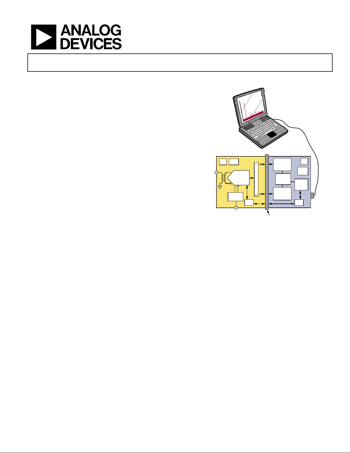
High Speed ADC USB FIFO Evaluation Kit
HSC-ADC-EVALB-SC/HSC-ADC-EVALB-DC
Rev. 0
Information furnished by Analog Devices is believed to be accurate and reliable. However, no
responsibility is assumed by Anal og Devices for its use, nor for any infringements of patents or ot her
rights of third parties that may result from its use. Specifications subject to change without notice. No
license is granted by implication or otherwise under any patent or patent rights of Analog Devices.
Trademarks and registered trademarks are the property of their respective owners.
One Technology Way, P.O. Box 9106, Norwood, MA 02062-9106, U.S.A.
Tel: 781.329.4700 www.analog.com
Fax: 781.461.3113 ©2006 Analog Devices, Inc. All rights reserved.
FEATURES
Buffer memory board for capturing digital data
used with high speed ADC evaluation boards
to simplify evaluation
32 kB FIFO depth at 133 MSPS (upgradable)
Measures performance with ADC Analyzer™
Real-time FFT and time domain analysis
Analyzes SNR, SINAD, SFDR, and harmonics
Simple USB port interface (2.0)
Supporting ADCs with serial port interfaces (SPI®)
On-board regulator circuit, no power supply required
6 V, 2 A switching power supply included
Compatible with Windows® 98 (2nd ed.), Windows 2000,
Windows Me, and Windows XP
EQUIPMENT NEEDED
Analog signal source and antialiasing filter
Low jitter clock source
High speed ADC evaluation board and ADC data sheet
PC running Windows 98 (2nd ed.), Windows 2000,
Windows Me, or Windows XP
Latest version of ADC Analyzer
USB 2.0 port recommended (USB 1.1-compatible)
PRODUCT DESCRIPTION
The high speed ADC FIFO evaluation kit includes the latest
version of ADC Analyzer and a buffer memory board to capture
blocks of digital data from the Analog Devices high speed
analog-to-digital converter (ADC) evaluation boards. The FIFO
board is connected to the PC through a USB port and is used
with ADC Analyzer to quickly evaluate the performance of high
speed ADCs. Users can view an FFT for a specific analog input
and encode rate to analyze SNR, SINAD, SFDR, and harmonic
information.
The evaluation kit is easy to set up. Additional equipment needed
includes an Analog Devices high speed ADC evaluation board,
a signal source, and a clock source. Once the kit is connected
and powered, the evaluation is enabled instantly on the PC.
Two versions of the FIFO are available. The HSC-ADC-EVALB-
DC is used with multichannel ADCs and converters with demulti-
plexed digital outputs. The HSC-ADC-EVALB-SC evaluation
board is used with single-channel ADCs. See
Table 1 to choose
the FIFO appropriate for your high speed ADC evaluation
board.
FUNCTIONAL BLOCK DIAGRAM
CLOCK INP UT
FILTERED
ANALOG
INPUT
SINGLE OR DUAL
HIGH-SPEED ADC
EVALUATION BOARD
120-PIN CO NNECTOR
HSC-ADC-EVALB-SC
OR
HSC-ADC-EVAL B-DC
CLOCK
CIRCUIT
LOGIC
SPI
ADC
n
n
SPI
+3.0V
REG
PS
CHB FIFO,
32K,
133MHz
TIMING
CIRCUIT
CHA FIFO,
32K,
133MHz
USB
CTLR
PS REG
STANDARD
USB 2.0
05870-001
Figure 1.
PRODUCT HIGHLIGHTS
1. Easy to Set Up. Connect the included power supply and
signal sources to the two evaluation boards. Then connect
to the PC and evaluate the performance instantly.
2. ADIsimADC™. ADC Analyzer supports virtual ADC
evaluation using ADI proprietary behavioral modeling
technology. This allows rapid comparison between multiple
ADCs, with or without hardware evaluation boards. For more
information, see AN-737 at
www.analog.com/ADIsimADC.
3. USB Port Connection to PC. PC interface is a USB 2.0
connection (1.1-compatible) to the PC. A USB cable is
provided in the kit.
4. 32 kB FIFO. The FIFO stores data from the ADC for processing.
A pin-compatible FIFO family is used for easy upgrading.
5. Up to 133 MSPS Encode Rate on Each Channel. Single-
channel ADCs with encode rates up to 133 MSPS can be used
with the FIFO board. Multichannel and demultiplexed output
ADCs can also be used with the FIFO board with clock rates
up to 266 MSPS.
6. Supports ADC with Serial Port Interface or SPI. Some ADCs
include a feature set that can be changed via the SPI. The FIFO
supports these SPI-driven features through the existing USB
connection to the computer without additional cabling needed.

HSC-ADC-EVALB-SC/HSC-ADC-EVALB-DC
Rev. 0 | Page 2 of 28
TABLE OF CONTENTS
Features .............................................................................................. 1
Equipment Needed........................................................................... 1
Product Description ......................................................................... 1
Functional Block Diagram .............................................................. 1
Product Highlights........................................................................... 1
Revision History ............................................................................... 2
FIFO Evaluation Board Easy Start.................................................. 3
Requirements ................................................................................ 3
Easy Start Steps ............................................................................. 3
Virtual Evaluation Board Easy Start With ADIsimADC ............ 4
Requirements ................................................................................ 4
Easy Start Steps ............................................................................. 4
FIFO 4.1 Data Capture Board Features ......................................... 5
FIFO 4.1 Supported ADC Evaluation Boards .......................... 6
Theory of Operation ........................................................................ 9
Clocking Description................................................................... 9
SPI Description ............................................................................. 9
Clocking with Interleaved Data................................................ 10
Connecting to the HSC-ADC-FPGA-4/-8 ............................. 10
Connecting to the DEMUX BRD ............................................ 10
Upgrading FIFO Memory ......................................................... 10
Jumpers ............................................................................................ 11
Default Settings........................................................................... 11
Evaluation Board ............................................................................ 13
Power Supplies ............................................................................ 13
Connection and Setup ............................................................... 13
FIFO Schematics and PCB Layout............................................... 14
Schematics................................................................................... 14
PCB Layout ................................................................................. 21
Bill of Materials ............................................................................... 23
Ordering Information.................................................................... 25
Ordering Guide .......................................................................... 25
ESD Caution................................................................................ 25
REVISION HISTORY
2/06—Revision 0: Initial Version

HSC-ADC-EVALB-SC/HSC-ADC-EVALB-DC
Rev. 0 | Page 3 of 28
FIFO EVALUATION BOARD EASY START
REQUIREMENTS
• FIFO evaluation board, ADC Analyzer, and USB cable
• High speed ADC evaluation board and ADC data sheet
• Power supply for ADC evaluation board
• Analog signal source and appropriate filtering
• Low jitter clock source applicable for specific ADC
evaluation, typically <1 ps rms
• PC running Windows 98 (2nd ed.), Windows 2000,
Windows Me, or Windows XP
• PC with a USB 2.0 port recommended (USB 1.1-
compatible)
EASY START STEPS
Note: You need administrative rights for the Windows
operating systems during the entire easy start procedure.
It is recommended to complete every step before reverting
to a normal user mode.
1. Install ADC Analyzer from the CD provided in the FIFO
evaluation kit or download the latest version on the Web.
For the latest updates to the software, check the Analog
Devices website at
www.analog.com/hsc-FIFO.
2. Connect the FIFO evaluation board to the ADC evaluation
board. If an adapter is required, insert the adapter between
the ADC evaluation board and the FIFO board. If using
the HSC-ADC-EVALB-SC model, connect the evaluation
board to the bottom two rows of the 120-pin connector,
closest to the installed IDT FIFO chip. If using an ADC
with a SPI interface, remove the two 4-pin corner keys so
that the third row can be connected.
3. Connect the provided USB cable to the FIFO evaluation
board and to an available USB port on the computer.
4. Refer to
Table 5 for any jumper changes. Most evaluation
boards can be used with the default settings.
5. After verification, connect the appropriate power supplies
to the ADC evaluation boards. The FIFO evaluation board
is supplied with a wall mount switching power supply that
provides a 6 V, 2 A maximum output. Connect the supply
end to the rated 100 ac to 240 ac wall outlet at 47 Hz to
63 Hz. The other end is a 2.1 mm inner diameter jack that
connects to the PCB at J301. Refer to the instructions
included in the
ADC data sheet for more information
about the ADC evaluation board’s power supply and other
requirements.
6. Once the cable is connected to both the computer and the
FIFO board, and power is supplied, the USB drivers start
to install. To complete the total installation of the FIFO
drivers, you need to complete the new hardware sequence
two times. The first Found New Hardware Wizard opens
with the text message This wizard helps you install
software for…Pre-FIFO 4.1. Click the recommended
install, and go to the next screen. A hardware installation
warning window should then be displayed. Click Continue
Anyway. The next window that opens should finish the Pre-
FIFO 4.1 installation. Click Finish. Your computer should
go through a second Found New Hardware Wizard, and
the text message, This wizard helps you install software
for…Analog Devices FIFO 4.1, should be displayed.
Continue as you did in the previous installation and click
Continue Anyway. Then click Finish on the next two
windows. This completes the installation.
7. (Optional) Verify in the device manager that Analog
Devices, FIFO4.1 is listed under the USB hardware.
8. Apply power to the evaluation board and check the voltage
levels at the board level.
9. Connect the appropriate analog input (which should be
filtered with a band-pass filter) and low jitter clock signal.
Make sure the evaluation boards are powered on before
connecting the analog input and clock.
10. Start ADC Analyzer.
11. Choose an existing configuration file for the ADC
evaluation board or create one.
12. Click Time Data in ADC Analyzer (left-most button under
the menus). A reconstruction of the analog input is
displayed. If the expected signal does not appear, or if there
is only a flat red line, refer to the ADC Analyzer data sheet
at
www.analog.com/hsc-FIFO for more information.

HSC-ADC-EVALB-SC/HSC-ADC-EVALB-DC
Rev. 0 | Page 4 of 28
VIRTUAL EVALUATION BOARD EASY START WITH ADIsimADC
REQUIREMENTS
Requirements include
• Completed installation of ADC Analyzer, Version 4.5.17 or
later.
• ADIsimADC product model files for the desired converter.
Models are not installed with the software, but they can be
downloaded from the
ADIsimADC Virtual Evaluation
Board website
at no charge.
No hardware is required. However, if you wish to compare
results of a real evaluation board and the model, you can switch
easily between the two, as outlined in the following
Easy Start
Steps
section.
EASY START STEPS
1. To get ADC model files, go to www.analog.com/ADIsimADC
for the product of interest. Download the product of
interest to a local drive. The default location is
c:\program
files\adc_analyzer\models
.
2. Start ADC Analyzer (see the
ADC Analyzer User Manual).
3. From the menu, click Config > Buffer > Model as the
buffer memory. In effect, the model functions in place of
the ADC and data capture hardware.
4. After selecting the model, click the Model button (located
next to the Stop button) to select and configure which
converter is to be modeled. A dialog box appears in the
workspace, where you can select and configure the
behavior of the model.
5. In the ADC Modeling dialog box, click the Device tab and
then click the
… (Browse) button, adjacent to the dialog
box. This opens a file browser and displays all of the
models found in the default directory: c:\program
files\adc_analyzer\models. If no model files are found,
follow the on-screen directions or see Step 1 to install
available models. If you have saved the models somewhere
other than the default location, use the browser to navigate
to that location and select the file of interest.
6. From the menu, click Config > FFT. In the FFT
Configuration dialog box, ensure that the Encode
Frequency is set for a valid rate for the simulated device
under test. If set too low or too high, the model does not run.
7. Once a model has been selected, information about the
model displays on the Device tab of the ADC Modeling
dialog box. After ensuring that you have selected the right
model, click the Input tab. This lets you configure the
input to the model. Click either Sine Wave or Two Tone
for the input signal.
8. Click Time Data (left-most button under the pull-down
menus). A reconstruction of the analog input is displayed.
The model can now be used just as a standard evaluation
board would be.
9. The model supports additional features not found when
testing a standard evaluation board. When using the
modeling capabilities, it is possible to sweep either the
analog amplitude or the analog frequency. For more
information consult the
ADC Analyzer User Manual at
www.analog.com/hsc-FIFO.
HSC-ADC-EVALB-SC/HSC-ADC-EVALB-DC
Rev. 0 | Page 5 of 28
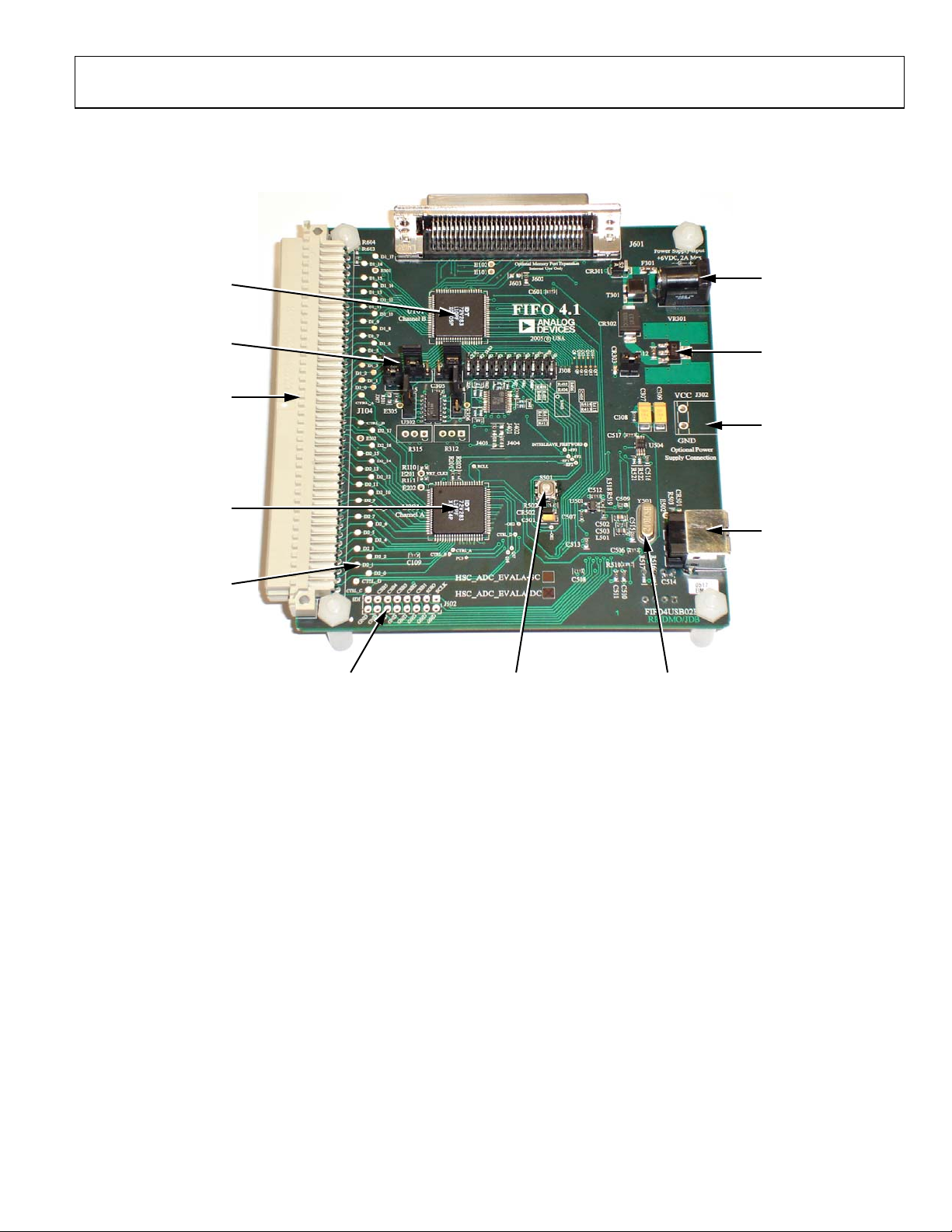
FIFO 4.1 DATA CAPTURE BOARD FEATURES
6V SWITCHING
POWER SUPPLY
CONNECTION
ON BOARD +3.3V
REGULATOR
OPTIONAL POWER
CONNECTION
USB CONNECTION
TO COMPUTER
µCONTROLLER CRYSTAL
CLOCK = 24MHz,
OFF DURING
DATA CAPTURE
RESET SWITCH
WHEN ENCODE RATE
IS INTERRUPTED
OPTIONAL SERIAL
PORT INTERFACE
CONNECTOR
OPEN SOLDER MASK
ON ALL DATA AND
CLOCK LINES FOR
EASY PROBING
IDT72V283 32k ⋅
16-BIT 133MHz FIFO
120-CONNECTOR
(PARALLEL CMOS
INPUTS)
TIMING ADJUSTMENT
JUMPERS
IDT72V283 32k ⋅
16-BIT 133MHz FIFO
05870-002
Figure 2. FIFO Components (Top View)
HSC-ADC-EVALB-SC/HSC-ADC-EVALB-DC
Rev. 0 | Page 6 of 28
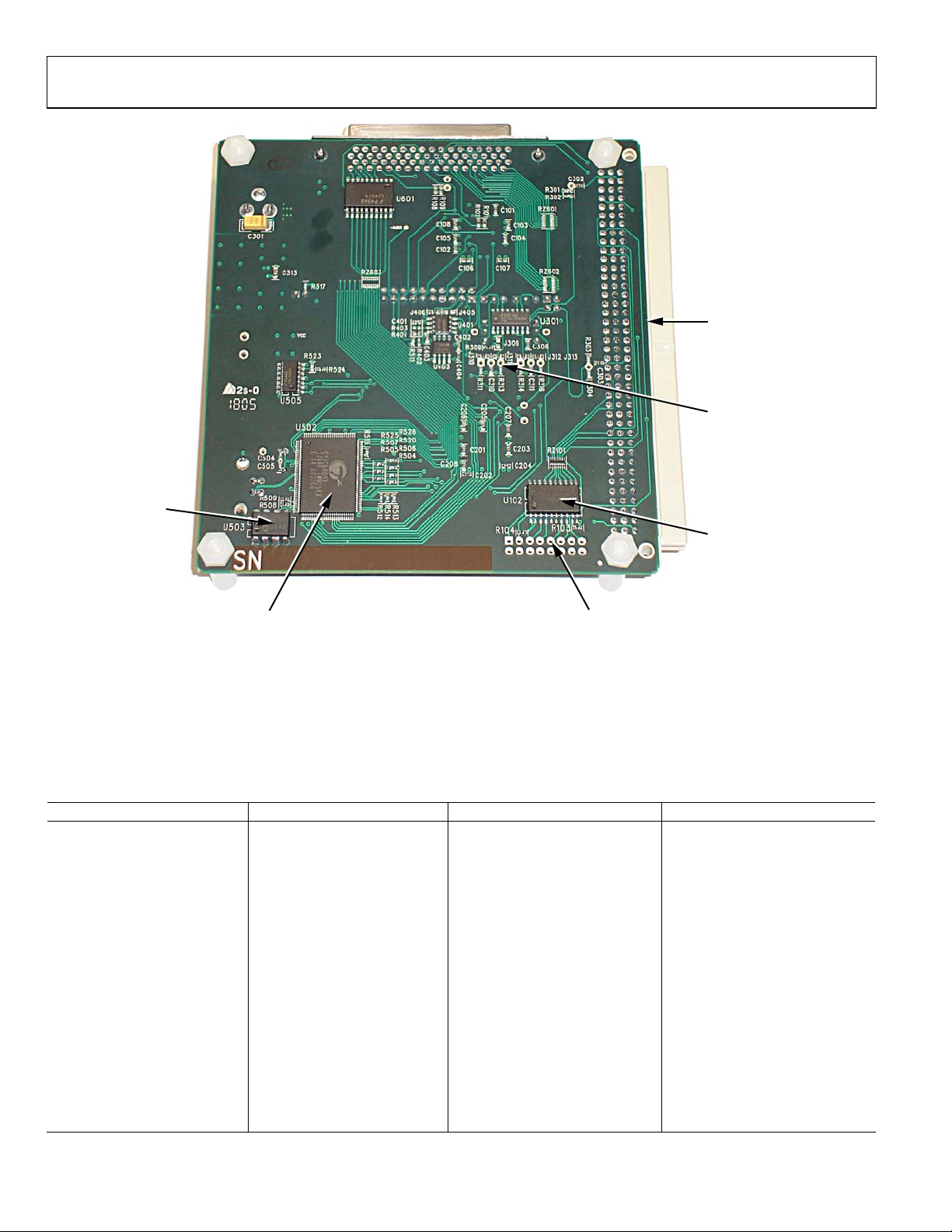
120-CONNECTOR
(PARALLEL CMOS
INPUTS)
TIMING ADJUSTMENT
JUMPERS
DRIVER CIRCUIT FOR
SERIAL PORT INTERFACE
(SPI) LINES
OPTIONAL SERIAL
PORT INTERFACE
(SPI) CONNECTOR
CYPRESS Fx2 HIGH SPEED
USB 2.0 µCONTROLLER
EPROM TO LOAD
USB FIRMWARE
05870-003
Figure 3. FIFO Components (Bottom View)
FIFO 4.1 SUPPORTED ADC EVALUATION BOARDS
The evaluation boards in Tab l e 1 can be used with the high speed ADC FIFO evaluation kit. Some evaluation boards require an adapter between
the ADC evaluation board connector and the FIFO connector. If an adapter is needed, send an email to
highspeed.converters@analog.com with
the part number of the adapter and a mailing address.
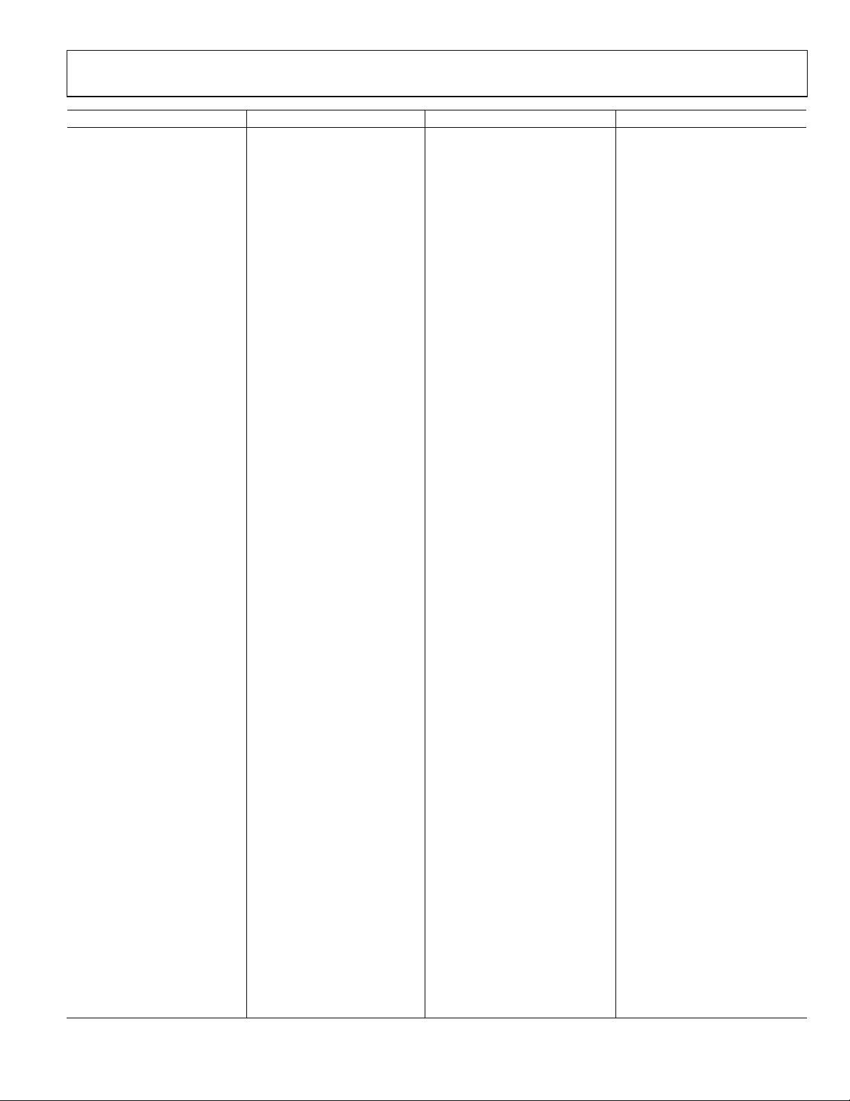
Table 1. HSC-ADC-EVALB-DC- and HSC-ADC-EVALB-SC-Compatible Evaluation Boards
1
Evaluation Board Model Description of ADC FIFO Board Version Comments
AD6644ST/PCB 14-bit, 65 MSPS ADC SC
AD6645-80/PCB
14-bit, 80 MSPS ADC SC
AD6645-105/PCB 14-bit, 105 MSPS ADC SC
AD9051/PCB 10-bit, 60 MSPS ADC SC Requires AD9051FFA
AD9200SSOP-EVAL 10-bit, 20 MSPS ADC SC Requires AD922xFFA
AD9200TQFP-EVAL 10-bit, 20 MSPS ADC SC Requires AD922xFFA
AD9201-EVAL Dual 10-bit, 20 MSPS ADC
1
SC Requires AD922xFFA
AD9203-EB 10-bit, 40 MSPS ADC SC Requires AD922xFFA
AD9212-65EB
1
Octal 10-bit, 65 MSPS ADC DC Requires HSC-ADC-FPGA-8
AD9215BCP-65EB 10-bit, 65 MSPS ADC SC
AD9215BCP-80EB 10-bit, 80 MSPS ADC SC
AD9215BCP-105EB 10-bit, 105 MSPS ADC SC
AD9215BRU-65EB 10-bit, 65 MSPS ADC SC
AD9215BRU-80EB 10-bit, 80 MSPS ADC SC
AD9215BRU-105EB 10-bit, 105 MSPS ADC SC
AD9216-80PCB Dual 10-bit, 80 MSPS ADC DC
AD9216-105PCB Dual 10-bit, 105 MSPS ADC DC
HSC-ADC-EVALB-SC/HSC-ADC-EVALB-DC
Rev. 0 | Page 7 of 28
Evaluation Board Model Description of ADC FIFO Board Version Comments
AD9218-105PCB 10-bit, 105 MSPS ADC DC
AD9218-65PCB 10-bit, 65 MSPS ADC DC
AD9219-65EB
1
Quad 10-bit, 65 MSPS ADC DC Requires HSC-ADC-FPGA-4/-8
AD9220-EB 12-bit, 10 MSPS ADC SC Requires AD922xFFA
AD9222-65EB
1
Octal 12-bit, 65 MSPS ADC DC Requires HSC-ADC-FPGA-8
AD9226-EB 12-bit, 65 MSPS ADC SC Requires AD922xFFA
AD9226QFP-EB 12-bit, 65 MSPS ADC SC Requires AD922xFFA
AD9228-65EB
1
Quad 12-bit, 65 MSPS ADC DC Requires HSC-ADC-FPGA-4/-8
AD9229-65EB
1
Quad 12-bit, 65 MSPS ADC DC Requires HSC-ADC-FPGA-4/-8
AD9233-80EB 12-bit, 80MSPS ADC SC
AD9233-105EB 12-bit, 105MSPS ADC SC
AD9233-125EB 12-bit, 125MSPS ADC SC
AD9234-EB 12-bit, 150MSPS ADC SC
AD9235BCP-20EB 12-bit, 20 MSPS ADC SC
AD9235BCP-40EB 12-bit, 40 MSPS ADC SC
AD9235BCP-65EB 12-bit, 65 MSPS ADC SC
AD9235-20PCB 12-bit, 20 MSPS ADC SC
AD9235-40PCB 12-bit, 40 MSPS ADC SC
AD9235-65PCB 12-bit, 65 MSPS ADC SC
AD9236BRU-80EB 12-bit, 80 MSPS ADC SC
AD9236BCP-80EB 12-bit, 80 MSPS ADC SC
AD9237BCP-20EB 12-bit, 20 MSPS ADC SC
AD9237BCP-40EB 12-bit, 40 MSPS ADC SC
AD9237BCP-65EB 12-bit, 65 MSPS ADC
SC
AD9238BST-20PCB Dual 12-bit, 20 MSPS ADC DC
AD9238BST-40PCB Dual 12-bit, 40 MSPS ADC DC
AD9238BST-65PCB Dual 12-bit, 65 MSPS ADC DC
AD9238BCP-20EB Dual 12-bit, 20 MSPS ADC DC
AD9238BCP-40EB Dual 12-bit, 40 MSPS ADC DC
AD9238BCP-65EB Dual 12-bit, 65 MSPS ADC DC
AD9240-EB 14-bit, 40 MSPS ADC SC Requires AD922xFFA
AD9241-EB 14-bit, 1.25 MSPS ADC SC Requires AD922xFFA
AD9243-EB 14-bit, 3 MSPS ADC SC Requires AD922xFFA
AD9244-40PCB 14-bit, 40 MSPS ADC SC
AD9244-65PCB 14-bit, 65 MSPS ADC SC
AD9245BCP-20EB 14-bit, 20 MSPS ADC
SC
AD9245BCP-40EB 14-bit, 40 MSPS ADC
SC
AD9245BCP-65EB 14-bit, 65 MSPS ADC
SC
AD9245BCP-80EB 14-bit, 80 MSPS ADC
SC
AD9246-80EB 14-bit, 80 MSPS ADC
SC
AD9246-105EB 14-bit, 105 MSPS ADC
SC
AD9246-125EB 14-bit, 125 MSPS ADC
SC
AD9248BST-65EB Dual 14-bit, 65 MSPS ADC DC
AD9248BCP-20EB Dual 14-bit, 20 MSPS ADC DC
AD9248BCP-40EB Dual 14-bit, 40 MSPS ADC DC
AD9248BCP-65EB Dual 14-bit, 65 MSPS ADC DC
AD9259-50EB
1
Quad 14-bit, 50 MSPS ADC DC Requires HSC-ADC-FPGA-4/-8
AD9260-EB 16-bit, 2.5 MSPS ADC SC Requires AD922xFFA
AD9280-EB 8-bit, 32 MSPS ADC SC Requires AD922xFFA
AD9281-EB Dual 8-bit, 28 MSPS ADC SC Requires AD922xFFA
AD9283/PCB 8-bit, 100 MSPS ADC SC Requires AD9283FFA
AD9287-100EB
1
Quad 8-bit, 100 MSPS ADC DC Requires HSC-ADC-FPGA-4/-8
AD9289-65EB
1
Quad 8-bit, 65 MSPS ADC DC Requires HSC-ADC-FPGA-9289
AD9411/PCB 10-bit, 200 MSPS ADC DC Requires DEMUX BRD

HSC-ADC-EVALB-SC/HSC-ADC-EVALB-DC
Rev. 0 | Page 8 of 28
Evaluation Board Model Description of ADC FIFO Board Version Comments
AD9430-CMOS/PCB 12-bit, 210 MSPS ADC DC
AD9430-LVDS/PCB
2
12-bit, 210 MSPS ADC DC Requires DEMUX BRD
AD9432/PCB 12-bit, 105 MSPS ADC SC
AD9433/PCB 12-bit, 125 MSPS ADC SC
AD9444-CMOS/PCB 14 bit, 80 MSPS ADC SC
AD9444-LVDS/PCB 14 bit, 80 MSPS ADC SC
AD9445-IF-LVDS/PCB 14-bit, 125 MSPS ADC SC
AD9445-BB-LVDS/PCB 14-bit, 125 MSPS ADC SC
AD9446-80LVDS/PCB 16-bit, 80 MSPS ADC SC
AD9446-100LVDS/PCB 16-bit, 100 MSPS ADC SC
AD9460-80EB-IF 16-bit, 80 MSPS ADC SC
AD9460-80EB-BB 16-bit, 80 MSPS ADC SC
AD9460-105EB-IF 16-bit, 105 MSPS ADC SC
AD9460-105EB-BB 16-bit, 105 MSPS ADC SC
AD9461-130EB-IF 16-bit, 130 MSPS ADC SC
AD9461-130EB-BB 16-bit, 130 MSPS ADC SC
AD9480-LVDS/PCB
2
8-bit, 250 MSPS ADC DC Requires DEMUX BRD
AD9481-PCB 8-bit, 250 MSPS ADC DC
AD10200/PCB Dual 12-bit, 105 MSPS ADC DC Requires GS09066
AD10201/PCB Dual 12-bit, 105 MSPS ADC DC Requires GS09066
AD10226/PCB Dual 12-bit, 125 MSPS ADC DC Requires GS09066
AD10265/PCB Dual 12-bit, 65 MSPS ADC DC Requires GS09066
AD10465/PCB Dual 14-bit, 65 MSPS ADC DC Requires GS09066
AD10677/PCB 16-bit, 65 MSPS ADC SC Requires GS09066
AD10678/PCB 16-bit, 80 MSPS ADC SC Requires GS09066
AD15252/PCB 12-bit, Dual 65 MSPS ADC DC
AD15452/PCB 12-bit, Quad 65 MSPS ADC DC Requires HSC-ADC-FPGA-4/-8
1
The high speed ADC FIFO evaluation kit can be used to evaluate two channels at a time.
2
If a DEMUX BRD is needed, send an email to highspeed.converters@analog.com.

HSC-ADC-EVALB-SC/HSC-ADC-EVALB-DC
Rev. 0 | Page 9 of 28
THEORY OF OPERATION
The FIFO evaluation board can be divided into several circuits,
each of which plays an important part in acquiring digital data
from the ADC and allows the PC to upload and process that
data. The evaluation kit is based around the IDT72V283 FIFO
chip from Integrated Device Technology, Inc (IDT). The system
can acquire digital data at speeds up to 133 MSPS and data
record lengths up to 32 kB using the HSC-ADC-EVALB-SC
FIFO evaluation kit. The HSC-ADC-EVALB-DC, which has
two FIFO chips, is available to evaluate multichannel ADCs or
demultiplexed data from ADCs sampling faster than 133 MSPS.
A USB 2.0 microcontroller communicating with ADC Analyzer
allows for easy interfacing to newer computers using the USB 2.0
(USB 1.1-compatible) interface.
The process of filling the FIFO chip or chips and reading the
data back requires several steps. First, ADC Analyzer initiates
the FIFO chip fill process. The FIFO chips are reset, using a
master reset signal (MRS). The USB microcontroller is then
suspended, which turns off the USB oscillator and ensures that
it does not add noise to the ADC input. After the FIFO chips
completely fill, the full flags from the FIFO chips send a signal
to the USB microcontroller to wake up the microcontroller
from suspend. ADC Analyzer waits for approximately 30 ms
and then begins the readback process.
During the readback process, the acquisition of data from
FIFO 1 (U201) or FIFO 2 (U101) is controlled via Signal OEA
and Signal OEB. Because the data outputs of both FIFO chips
drive the same 16-bit data bus, the USB microcontroller
controls the OEA and OEB signals to read data from the correct
FIFO chip. From an application standpoint, ADC Analyzer
sends commands to the USB microcontroller to initiate a read
from the correct FIFO chip, or from both FIFO chips in dual or
demultiplexed mode.
CLOCKING DESCRIPTION
Each channel of the buffer memory requires a clock signal to
capture data. These clock signals are normally provided by the
ADC evaluation board and are passed along with the data
through Connector J104 (Pin 37 for both Channel A and
Channel B). If only a single clock is passed for both channels,
they can be connected together by Jumper J303.
Jumpers J304 and J305 at the output of the LVDS receiver allow
the output clock to be inverted by the LVDS receiver. By default,
the clock outputs are inverted by the LVDS receiver.
The single-ended clock signal from each data channel is
buffered and converted to a differential CMOS signal by two
gates of a low voltage differential signal (LVDS) receiver, U301.
This allows the clock source for each channel to be CMOS,
TTL, or ECL.
The clock signals are ac-coupled by 0.1 μF capacitors.
Potentiometer R312 and Potentiometer R315 allow for fine
tuning the threshold of the LVDS gates. In applications where
fine-tuning the threshold is critical, these potentiometers can be
replaced with a higher resistance value to increase the
adjustment range. Resistors R301, R302, R303, R304, R311,
R313, R314, and R316 set the static input to each of the
differential gates to a dc voltage of approximately 1.5 V.
At assembly, Solder Jumper J310 to Solder Jumper J313 are set
to bypass the potentiometer. For fine adjustment using the pot,
the solder jumpers must be removed, and R312 and R315 must
be populated.
U302, an XOR gate array, is included in the design to let users
add gate delays to the FIFO memory chip clock paths. They are
not required under normal conditions and are bypassed at
assembly by Jumper J314 and Jumper J315. Jumper J306 and
Jumper J307 allow the clock signals to be inverted through an
XOR gate. In the default setting, the clocks are not inverted by
the XOR gate.
The clock paths described above determine the WRT_CLK1 and
WRT_CLK2 signals at each FIFO memory chip (U101 and
U201). The timing options above should let you choose a clock
signal that meets the setup and hold time requirements to
capture valid data.
A clock generator can be applied directly to S1 and/or S3. This
clock generator should be the same unit that provides the clock
for the ADC. These clock paths are ac-coupled, so that a sine
wave generator can be used. DC bias can be adjusted by
R301/R302 and R303/R304.
The DS90LV048A differential line receiver is used to square the
clock signal levels applied externally to the FIFO evaluation
board. The output of this clock receiver can either directly drive
the write clock of the IDT72V283 FIFO(s), or first pass through
the XOR gate timing circuitry described above.
SPI DESCRIPTION
The Cypress IC (U502) supports the HSC SPI standard to allow
programming of ADCs that have SPI-accessible register maps.
U102 is a buffer that drives the 4-wire SPI (SCLK, SDI, SDO,
CSB
1
) through the 120-pin connector (J104) on the third or top
row. J502 is an auxiliary SPI connector to monitor the SPI
signals connected directly to the Cypress IC. For more
information on this and other functions, consult the user
manual titled Interfacing to High Speed ADCs via SPI at
www.analog.com/hsc-FIFO.
1
Note that CSB1 is the default CSB line used.
Loading...