


EE-68
Table of contents
 Loading...
Engineer-to-Engineer Note EE-68
a
Technical notes on using Analog Devices DSPs, processors and development tools
Contact our technical support at dsp.support@analog.com and at dsptools.support@analog.com
Or vi sit our o n-li ne r esou rces htt p:/ /www.analog.com/ee-notes and http://www.analog.com/processors
Analog Devices JTAG Emulation Technical Reference
Contributed by David M. Doyle Rev 9 – October 18, 2004
Copyright 2004, Analog Devices, Inc. All rights reserved. Analog Devices assumes no responsibility for customer product design or the use or application of
customers’ products or for any infringements of patents or rights of others, which may result from Analog Devices assistance. All trademarks and logos are property
of their respective holders. Information furnished by Analog Devices Applications and Development Tools Engineers is believed to be accurate and reliable;
however, no responsibility is assumed by Analog Devices regarding the technical accuracy and topicality of the content provided in all Analog Devices’ Engineer-to-
Engineer Notes.
Introduction
This document provides technical information to
properly design a JTAG emulator interface for
Analog Devices, Inc. (ADI) processor targets,
that in this document are all referred to as Digital
Signal Processors (DSPs).
ADI designs, manufactures, and sells several
different types of JTAG emulators for use with
ADI DSP targets supporting an embedded JTAG
emulator port. This document has been revised to
only support the current line of ADI emulators.
This product line includes the HPPCI, HPUSB
and USB emulators.
L
Table 4 explains in detail important
information referenced by a “Note n”
reference in figures and tables
throughout this document. You should
first review this table before continuing
with this document. Most questions
addressed by users regarding differences
with our JTAG emulator products and
previous versions of this document are
answered in this table.
Older versions of this document supported ADI
JTAG emulator legacy products. They included
the Mountain-ICE, Summit-ICE, Trek-ICE, Apex-
ICE, and EZ-ICE. If you require information for
any ADI JTAG emulators not supported in this
document, you should contact ADI’s DSP
development tools technical support for an older
revision of this document which contains legacy
JTAG emulator information.
L
Do not use older versions of EE-68 for
new target designs. Periodically check
ADI’s web site at
http://www.analog.com/ee-notes/
for newer revisions of this document.
Targets which were designed using an
older revision of EE-68 should only be
updated if there are problems
performing JTAG emulation.
JTAG Emulator Interface Design
All ADI JTAG emulators interface with the DSP
using a 14-pin JTAG emulator header. The
header provides a connection interface for the
JTAG emulator pod. The header can also be used
to route an optional local boundary scan
controller to the DSP when the JTAG emulator is
not attached.
All ADI JTAG emulators use a superset of the
IEEE 1149.1 standard to send and receive data
from the DSP JTAG emulation port. The JTAG
emulators use an additional signal called EMU~ as
a JTAG emulation status flag from the DSP. This
signal is a vendor specific signal, which is not
part of the IEEE 1149.1 specification.
The following pages will define in detail the
design requirements for supporting ADI JTAG
emulators. This information includes functional,
electrical, and mechanical requirements for
interfacing a target design with a JTAG
emulator.
a
Analog Devices JTAG Emulation Technical Reference (EE-68) Page 2 of 15
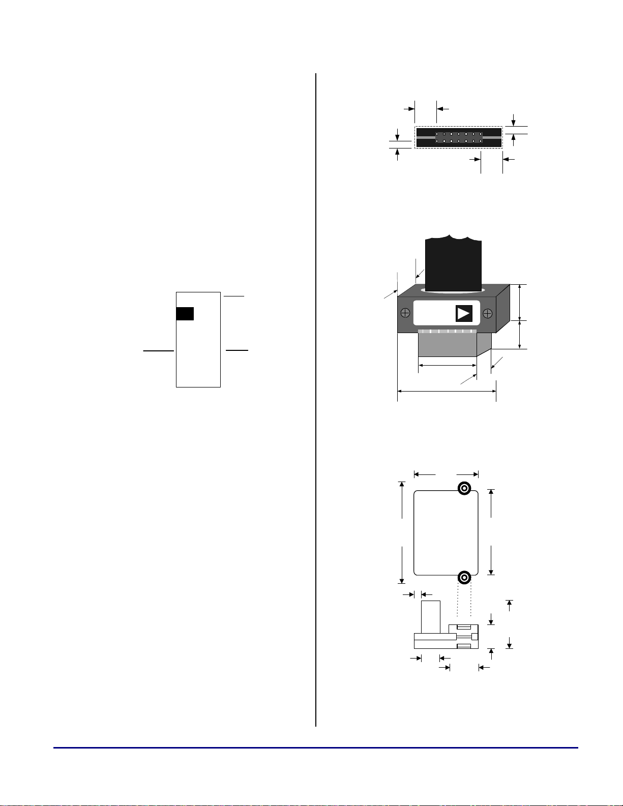
JTAG Emulator Target Header
Referring to Figure 1, the JTAG emulator header
has 14 pins. You must supply this header on your
target to communicate with the JTAG emulator.
The JTAG emulator target header interface is a
standard dual-row 0.025” male square-post
header, set on 0.1” x 0.1” spacing, with a
minimum post length of 0.235”. Pin 3 on the
JTAG emulator cable header is keyed to prevent
accidental insertion of the pod to the target
backwards. Clip pin 3 on your target board
header allow insertion of the JTAG emulator
cable female header.
(See Table 4 for notes)
GND
no pin (key)
BTMS/VDDIO
BTCK
BTDI
GND
EMU
BTRST
12
4
56
78
9
10
11 12
13 14
3
GND
TMS
TCK
TRST
TDI
TDO
See Note 2
See Notes 3, 4, 14
Figure 1. JTAG Emulator Target Header Interface
JTAG Emulator Pod Mechanical
Requirements
This section explains the mechanical
specifications for the JTAG emulator pod.
JTAG Emulator Header clearance requirements
Provide a clearance of at least 0.30” and 0.10”
around the length and width of the header. Refer
to Figure 2 for information about the pod
connector keep out area.
L
Make sure you allow for height
clearance above the header for attaching
and detaching the JTAG emulator cable
from your target.
Refer to Figure 3 for any height clearance
restriction information regarding the HPPCI
JTAG emulator cable. Refer to Figure 4 for any
height clearance restriction information for the
HPUSB and USB JTAG emulators.
(See Table 4 for notes)
0.30”
0.30”
0.10”
0.10”
Figure 2. JTAG Emulator Header Keep Out Area
(See Table 4 for notes)
ANALOG
DEVICES
0.70"
0.20"
1.19"
0.43"
0.29"
0.20"
0.28"
HPPCI
See Note 20
Figure 3. HPPCI JTAG Emulator Pod Dimensions
(See Table 4 for notes)
HPUSB
or
USB
0.668"
1.053"
0.878"
0.200"
0.065"
0.300"
0.500"
0.245"
See Note 21
Figure 4. HPUSB JTAG Emulator Pod Dimensions

a
Analog Devices JTAG Emulation Technical Reference (EE-68) Page 3 of 15
Local Boundary Scan Controller
Referring to Figure 1, the set of signals on the
odd-numbered side of the connector can be used
by targets which have an optional local boundary
scan controller. These signals include the
boundary-scan controller JTAG signals
BTMS/VDDIO, BTCK, BTDI, and BTRST~. Each of these
signals is described in Table 1.
Pin Signal Description Emulator Target
1 GND Digital Ground Passive Passive
2 EMU~ JTAG Emulation Flag Input
{active low}
Output
{open drain} {active
low}
3 KEY Header Alignment position -- pin must be
clipped on target header
See note 2
No Connect No Connect
4 GND Digital Ground Passive Passive
5 VDDIO
or
BTMS
Automatic Voltage Sense (VDDIO)
See note 3
or
Target Local Boundary Scan Controller
JTAG TAP Test Mode Select
Input Passive
or
Output
6 TMS JTAG TAP Test Mode Select Output Input
7 BTCK Target Local Boundary Scan Controller
JTAG TAP Test Clock
No Connect Output
8 TCK JTAG TAP Test Clock Output Input
9 BTRST~ Target Local Boundary Scan Controller
JTAG TAP Test Reset
No Connect Output
{active low}
10 TRST~ JTAG TAP Test Reset Output Input {active low}
11 BTDI Target Local Boundary Scan Controller
JTAG TAP Test Data In
No Connect Output
12 TDI JTAG TAP Test Data In Output Input
13 GND Digital Ground Passive Passive
14 TDO JTAG TAP Test Data Out Input Output
Table 1. JTAG Emulator Header Signal Descriptions
L
Only the HPPCI JTAG emulator
supports automatic voltage sensing with
pin 5. The USB and HPUSB JTAG
emulators pin 5 only supports the BTMS
functionality. See note 3 and note 4 in
Table 4 regarding special instructions
for pin 5.
Pin 5 (
BTMS/VDDIO) is a dual purpose pin. First, it
is used by the JTAG emulator to sense the DSP
IO voltage (
VDDIO). Second, it can be used to
route a local boundary scan controller BTMS
signal to the DSP
TMS pin when the JTAG
emulator is not connected.
The HPPCI JTAG emulator can automatically
sense a DSP IO voltage (VDDIO) up to 5 V. The
HPPCI JTAG emulator uses the VDDIO voltage it
senses from the
BTMS/VDDIO pin to adjust the
JTAG emulator interface input signal thresholds
and output signal drive levels to those shown in
Table 2. You must pull pin 5 (BTMS/VDDIO) up to

a
Analog Devices JTAG Emulation Technical Reference (EE-68) Page 4 of 15
the DSP IO voltage (VDDIO) with a 4.7 KΩ
resistor when using the HPPCI JTAG emulator.
See note 3 and note 4 in Table 4 regarding
special instructions for pin 5.
Targets with Local Boundary Scan Logic
Targets which use optional local boundary scan
controller logic should connect the local
boundary-scan signal pins to the JTAG emulator
header pins shown in Figure 5.
If your target has a optional local boundary scan
controller, and you attach the HPPCI JTAG
emulator, you will need to isolate BTMS signal
from the
BTMS/VDDIO voltage before starting the
emulator software. Referring to Figure 5 and
Figure 7, during JTAG emulation you can isolate
pin 5 on the HPPCI JTAG emulator header from
the local boundary scan controller logic using a
jumper or tri-state buffer. You must provide a
method to isolate the BTMS signal on your target
from the BTMS/VDDIO pin on the JTAG emulator
header when the HPPCI JTAG emulator is
connected. Isolation must be effective before the
HPPCI JTAG emulator software is invoked.
This isolation will prevent the local boundary
scan controller BTMS signal from confusing the
automatic voltage sensing logic in the HPPCI
JTAG emulator pod.
Connections are made between the local
boundary scan controller and the DSP by
installing or removing jumpers between the local
boundary scan controller JTAG signals and the
DSP JTAG emulation signals. The local
boundary scan signals include BTMS, BTCK, BTDI,
and
BTRST~. DSP JTAG emulation signals TMS,
TCK, TDI, and TRST~ connect to local boundary
scan signals using jumpers on the JTAG
emulator header shown in Figure 5.
TRST~ must be pulsed low at power up when
using a local boundary scan controller, and
should be kept low when the local boundary scan
controller and the JTAG emulator are not being
used. Figure 5 shows how
TRST~ should be
controlled when the target uses a local boundary
scan controller.
If your target has a local boundary scan
controller and your target does not control the
BTRST~ signal, you will need to control the BTRST~
signal with additional logic. This additional logic
needs to guarantee the BTRST~ signal is only
pulsed low during power on reset. It should be
driven high all other times during local boundary
scan. This will prevent holding the BTRST~ signal
low continuously during local boundary scans.
Keeping the DSP TAP constantly in reset with
the BTRST~ signal forced to ground with a jumper
or pull-down resistor will prevent the DSP from
executing a local boundary scan.
Jumpers can be substituted with zero ohm
resistors on production boards. If you plan to use
the same board revision for debugging and
production, you should design your target with a
dual footprint. The dual footprint should
accommodate the header described in Figure 1
for debug version boards, and surface mount
resistors for production version boards.
With the exception of pin 5 (BTMS/VDDIO) on the
HPPCI JTAG emulator, all target local boundary
scan controller pins (BTCK, BTRST~, BTDI) are not
connected inside the JTAG emulator pod. They
are used only to provide a method for inserting
or removing the DSP from the local boundary-
scan controller logic using jumpers across the
JTAG emulation header.
Targets without Local Boundary Scan Logic
As shown in Figure 6 and Figure 8, targets which
do not use a local boundary scan controller, or do
not include the DSP in the local boundary scan
controller chain, should tie all boundary scan
pins to ground except for pin 5 on the HPPCI
JTAG emulator. Pin 5 the
BTMS/VDDIO signal, is
required by the HPPCI JTAG emulator pod to
automatically sense the DSP IO voltage (
VDDIO).
Jumpers can be substituted with zero ohm
resistors on production boards. If you plan to use
the same board revision for debugging and
a
Analog Devices JTAG Emulation Technical Reference (EE-68) Page 5 of 15
production, you should design your target with a
dual footprint. The dual footprint should
accommodate the header described in Figure 1
for debug boards, and surface mount resistors for
production boards.
Boundary Scan Controller
Target DSP VDDIO
4.7K
Boundary Scan Controller
Boundary Scan Controller
Buffer Enable Logic
BTMSOE
Target DSP
Target DSP
Target DSP
Target DSP
Target DSP
Target DSP
Power Up Reset Logic
Boundary Scan Reset Logic
BSCRST
PONRST
See Note 4
BTMS/VDDIO
GND
no pin (key)
BTCK
BTDI
GND
13 14
GND
TMS
TCK
TDI
TDO
EMU~
BTRST
TRST
11 12
910
78
56
3
4
12
See Note 5
See Note 6
See Note 7
See Note 4
See Note 12
See Notes 3, 4, 14
See Note 18
See Note 19
See Note 5
See Note 5
See Note 18
See Note 19
See Note 12
See Note 6
See Note 6
See Note 6
Figure 5. Single DSP Target with a Local Boundary Scan Controller
Target DSP VDDIO
4.7K
Target DSP
Target DSP
Target DSP
Target DSP
Target DSP
Target DSP
BTMS/VDDIO
GND
no pin (key)
BTCK
BTDI
GND
GND
TMS
TCK
TDI
TDO
BTRST
TRST
3
4
12
13 14
11 12
910
78
56
See Notes 3, 4, 14
EMU~
See Note 6
See Note 7
See Note 12
See Note 18
See Note 19
See Note 18
See Note 19
See Note 12
See Note 6
See Note 6
See Note 6
Figure 6. Single DSP Target without a Local Boundary Scan Controller
Single DSP Target Connections
Single DSP targets with route distances between
the JTAG emulator header and DSP less than six
(6) inches do not require buffering. Your target
requires buffering if the worst case route distance
between the JTAG emulator header and the DSP
is greater than six (6) inches regardless of the
number of DSPs in the scan chain path.
Figure 6 shows the connections between the
JTAG emulator header and the DSP for a single
DSP target without a local boundary scan
controller. Figure 5 shows the connections
between the JTAG emulator header and the DSP
for a single DSP target with a local boundary
scan controller.
Figure 5 and Figure 6 show series terminating
resistors for the
TDO and EMU~ signals going to the
JTAG emulator. These resistors are optional.
Loading...