


AD1816AJST

a
SoundPort® Controller
AD1816A
FEATURES
Compatible with Microsoft
®
PC 97 Logo Requirements
Supports Applications Written for Windows
Windows 3.1, Windows NT, SoundBlaster
AdLib
®
/OPL3
®
Stereo Audio 16-Bit SD Codec
Internal 3D Circuit—Phat™
Stereo Phase Expander
MPC Level-3 Mixer
ISA Plug and Play Compatible
16-Bit Address Decode
Dual Type F FIFO DMA Support
MPU-401 Compatible MIDI Port
Supports Wavetable Synthesizers
Integrated Enhanced Digital Game Port
Bidirectional DSP Serial Port
2
S Digital Audio Serial Ports
Two I
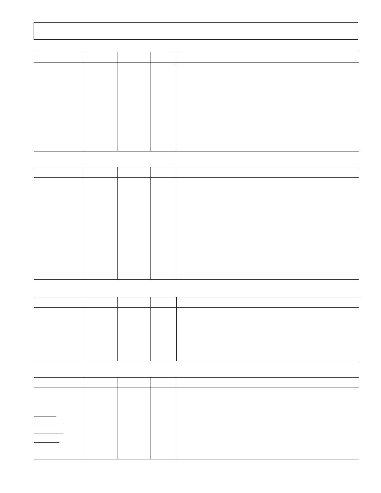
AD1816A
MIC
LINE
SYNTH
CD
VID
PHONE_IN
L_OUT
PHONE_OUT
R_OUT
MV
MV
MV
0dB/
20dB
Σ
Σ
A
M
Σ
PHAT
STEREO
Σ
Σ
PHAT
STEREO
G = GAIN
A = ATTENUATE
M = MUTE
MV = MASTER VOLUME
AGC
G
G
G
G
A
M
A
A
A
M
M
M
Σ
Σ
ΣΣ
Integrated OPL3 Compatible Music Synthesizer
®
95,
®
Pro,
Software and Hardware Volume Control
Full-Duplex Capture and Playback Operation at
Different Sample Rates
Supports Up to Six Different Sample Rates Simultaneously
1 Hz Resolution Programmable Sample Rates from
4 kHz to 55.2 kHz
Power Management Modes
Operation from +5 V Supply
Built-In 24 mA Bus Drivers
100-Lead PQFP and TQFP Package
FUNCTIONAL BLOCK DIAGRAM
VOL_DN
VOL_UP
HARDWARE
VOLUME
CONTROL
PGA
SELECTOR
G
A
M
Σ
16-BIT
SD D/A
CONVERTER
Σ
ΣΣΣΣΣ
SEL
XIRQ
MODEM/
LOGICAL
DEVICE
CONTROL
16-BIT
SD A/D
CONVERTER
Σ
Σ
OSCILLATORS
DATA
E2PROM
CONTROL
M A
M A
M A
M A
CLK
REGISTER
DSP SERIAL PORT
2
SB PRO
SERIAL PORT
INTERFACE
MIDI_IN
MPU-401
2
2
2
2
A_1
B_1
MIDI_OUT
GAME PORT
FORMAT
MUSIC
SYNTHESIZER
FORMAT
I2S SERIAL PORT (0)
I2S SERIAL PORT (1)
A_X
B_X
A_2
FIFO
FIFO
DIGITAL PLL
B_Y
A_Y
B_2
DRQ (X)
IRQ (X)
PC_D (7:0)
PC_A (15:0)
AEN
DACK (X)
PARALLEL INTERFACE
PLUG AND PLAY ISA BUS
IOR
IOW
BCLK (0)
LRCLK (0)
SDATA (0)
BCLK (1)
LRCLK (1)
SDATA (1)
PCLKO
SoundPort is a registered trademark of Analog Devices, Inc.
Phat is a trademark of Analog Devices, Inc.
All other trademarks are the property of their respective holders.
REV. A
Information furnished by Analog Devices is believed to be accurate and
reliable. However, no responsibility is assumed by Analog Devices for its
use, nor for any infringements of patents or other rights of third parties
which may result from its use. No license is granted by implication or
otherwise under any patent or patent rights of Analog Devices.
SDI
XTALO
XTALI
SDO
SDFS
SCLK
One Technology Way, P.O. Box 9106, Norwood, MA 02062-9106, U.S.A.
Tel: 781/329-4700 World Wide Web Site: http://www.analog.com
Fax: 781/326-8703 © Analog Devices, Inc., 1997

AD1816A
PRODUCT OVERVIEW
The AD1816A SoundPort Controller is a single chip Plug and
Play multimedia audio subsystem for concurrently processing
multiple digital streams of 16-bit stereo audio in personal computers. The AD1816A maintains full legacy compatibility with
applications written for SoundBlaster Pro and AdLib, while servic ing Microsoft PC 97 application requirements. The AD1816A
includes an internal OPL3 compatible music synthesizer, Phat
TABLE OF CONTENTS
FEATURES . . . . . . . . . . . . . . . . . . . . . . . . . . . . . . . . . . . . . 1
PRODUCT OVERVIEW . . . . . . . . . . . . . . . . . . . . . . . . . . . 2
SPECIFICATIONS . . . . . . . . . . . . . . . . . . . . . . . . . . . . . . . 3
PIN CONFIGURATION . . . . . . . . . . . . . . . . . . . . . . . . . . . 9
PIN FUNCTION DESCRIPTIONS . . . . . . . . . . . . . . . . . 11
HOST INTERFACE . . . . . . . . . . . . . . . . . . . . . . . . . . . . . 15
REFERENCES . . . . . . . . . . . . . . . . . . . . . . . . . . . . . . . . . . 16
SERIAL INTERFACES . . . . . . . . . . . . . . . . . . . . . . . . . . . 17
ISA INTERFACE . . . . . . . . . . . . . . . . . . . . . . . . . . . . . . . . 21
AD1816A Chip Registers . . . . . . . . . . . . . . . . . . . . . . . . . 21
AD1816A Plug and Play Device Configuration Registers . . 22
Sound System Direct Registers . . . . . . . . . . . . . . . . . . . . . 23
Sound System Indirect Registers . . . . . . . . . . . . . . . . . . . 29
SB Pro; AdLib Registers . . . . . . . . . . . . . . . . . . . . . . . . . . 38
MPU-401 Registers . . . . . . . . . . . . . . . . . . . . . . . . . . . . . 39
Game Port Register . . . . . . . . . . . . . . . . . . . . . . . . . . . . . 39
APPENDIX A.
PLUG AND PLAY INTERNAL ROM . . . . . . . . . . . . . . 40
PLUG AND PLAY KEY AND “ALTERNATE KEY”
SEQUENCES . . . . . . . . . . . . . . . . . . . . . . . . . . . . . . . 41
AD1816 AND AD1816A COMPATIBILITY . . . . . . . . . 42
USING AN EEPROM WITH THE AD1816 OR
AD1816A . . . . . . . . . . . . . . . . . . . . . . . . . . . . . . . . . . . 42
AD1816 FLAG BYTE . . . . . . . . . . . . . . . . . . . . . . . . . . . 42
USING THE AD1816 WITHOUT AN EEPROM . . . . . 42
AD1816A FLAG BYTES . . . . . . . . . . . . . . . . . . . . . . . . 43
USING THE AD1816A WITHOUT AN EEPROM . . . . 44
MAPPING THE AD1816 EEPROM INTO THE
AD1816A EEPROM . . . . . . . . . . . . . . . . . . . . . . . . . . 45
PIN MUXING IN THE AD1816 AND AD1816A . . . . . 45
PROGRAMMING EXTERNAL EEPROMS . . . . . . . . . 47
REFERENCE DESIGNS AND DEVICE DRIVERS . . . 47
OUTLINE DIMENSIONS . . . . . . . . . . . . . . . . . . . . . . . . . 50
Stereo circuitry for phase expanding the analog stereo output,
an MPU-401 UART, joystick interface with a built-in timer, a
DSP serial port and two I
Plug and Play routine provides configuration services for all integrated logical devices. Using an external E
2
S serial ports. The AD1816A on-chip
2
PROM allows the
AD1816A to decode up to two additional external user-defined
logical devices such as modem and CD-ROM.
Figures
Functional Block Diagram . . . . . . . . . . . . . . . . . . . . . . . . . . . 1
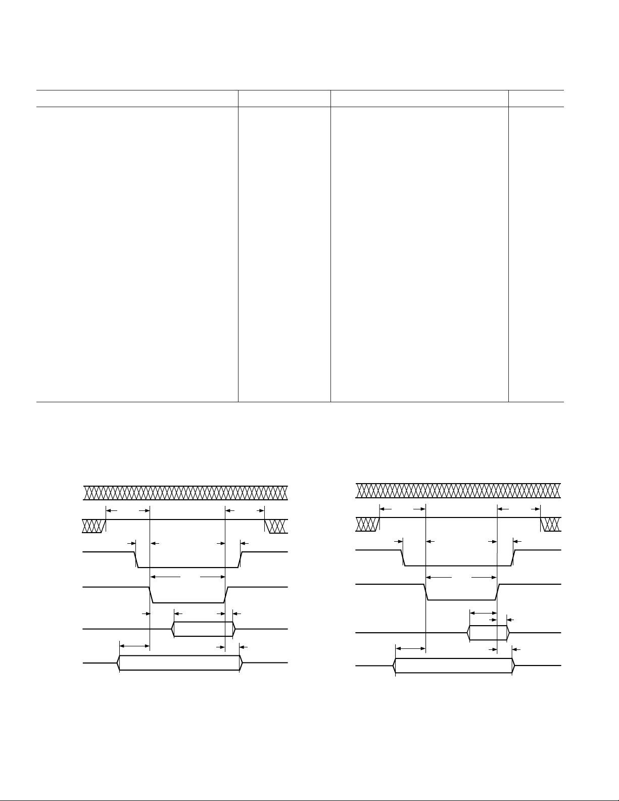
Figure 1. PIO Read Cycle . . . . . . . . . . . . . . . . . . . . . . . . . . . 6
Figure 2. PIO Write Cycle . . . . . . . . . . . . . . . . . . . . . . . . . . 6
Figure 3. DMA Read Cycle . . . . . . . . . . . . . . . . . . . . . . . . . 7
Figure 4. DMA Write Cycle . . . . . . . . . . . . . . . . . . . . . . . . . 7
Figure 5. Codec Transfers . . . . . . . . . . . . . . . . . . . . . . . . . . 7
Figure 6. DSP Port Timing . . . . . . . . . . . . . . . . . . . . . . . . . . 7
Figure 7. I
2
S Serial Port Timing . . . . . . . . . . . . . . . . . . . . . . 7
Figure 8. Reset Pulse Width . . . . . . . . . . . . . . . . . . . . . . . . . 7
Figure 9. Serial Interface Right-Justified Mode . . . . . . . . . . 17
Figure 10. Serial Interface I
2
S-Justified Mode . . . . . . . . . . . 17
Figure 11. Serial Interface Left-Justified Mode . . . . . . . . . . 17
Figure 12. DSP Serial Interface (Default Frame Rate) . . . . 20
Figure 13. DSP Serial Interface (User Programmed
Frame Rate) . . . . . . . . . . . . . . . . . . . . . . . . . . . . . . . . . . . 20
Figure 14. DSP Serial Port . . . . . . . . . . . . . . . . . . . . . . . . . 21
Figure 15. Codec Transfers . . . . . . . . . . . . . . . . . . . . . . . . . 27
Figure 16. Recommended Application Circuit . . . . . . . . . . 48
Figure 17. AD1816A Frequency Response Plots . . . . . . . . . 49
Tables
Table I. DSP Port Time Slot Map . . . . . . . . . . . . . . . . . . . 18
Table II. Chip Register Diagram . . . . . . . . . . . . . . . . . . . . . 21
Table III. Logical Devices and Compatible Plug and
Play Device Drivers . . . . . . . . . . . . . . . . . . . . . . . . . . . . . 22
Table IV. Internal Logical Device Configuration . . . . . . . . 23
Table V. Sound System Direct Registers . . . . . . . . . . . . . . . 23
Table VI. Codec Transfers . . . . . . . . . . . . . . . . . . . . . . . . . 27
Table VII. Indirect Register Map and Reset/Default States . 30
Table VIII. Sound System Indirect Registers . . . . . . . . . . . 31
Table IX. SoundBlaster Pro ISA Bus Registers . . . . . . . . . . 38
Table X. AdLib ISA Bus Registers . . . . . . . . . . . . . . . . . . . 39
Table XI. MIDI ISA Bus Registers . . . . . . . . . . . . . . . . . . . 39
Table XII. Game Port ISA Bus Registers . . . . . . . . . . . . . . 39
Table XIII. AD1816 Pin Muxing . . . . . . . . . . . . . . . . . . . . 45
Table XIV. AD1816A Pin Muxing . . . . . . . . . . . . . . . . . . . 46
–2–
REV. A

SPECIFICA TIONS
AD1816A
STANDARD TEST CONDITIONS UNLESS
OTHERWISE NOTED
Temperature 25 °C
Digital Supply (V
Analog Supply (V
Sample Rate (F
Input Signal Frequency 1008 Hz
Audio Output Passband 20 Hz to 20 kHz
V
IH
V
IL
ANALOG INPUT
Parameter Min Typ Max Units
Full-Scale Input Voltage (RMS Values Assume Sine Wave Input)
PHONE_IN, LINE, SYNTH, CD, VID 1 V rms
MIC with +20 dB Gain (MGE = 1) 0.1 V rms
MIC with 0 dB Gain (MGE = 0) 1 V rms
Input Impedance* 17 kΩ
Input Capacitance* 15 pF
) 5.0 V
DD
) 5.0 V
CC
) 48 kHz
S
5.0 V
0V
DAC Test Conditions
0 dB Attenuation
Input Full Scale
16-Bit Linear Mode
100 kΩ Output Load
Mute Off
Measured at Line Output
ADC Test Conditions
0 dB Gain
Input –4 dB Relative to Full Scale
Line Input Selected
16-Bit Linear Mode
2.83 V p-p
0.283 V p-p
2.83 V p-p
PROGRAMMABLE GAIN AMPLIFIER—ADC
Parameter Min Typ Max Units
Step Size (0 dB to 22.5 dB)
(All Steps Tested) 1.5 dB
PGA Gain Range Span 22.5 dB
CD, LINE, MICROPHONE, SYNTHESIZER, AND VIDEO INPUT ANALOG GAIN/ATTENUATORS/MUTE AT LINE OUTPUT
Parameter Min Typ Max Units
CD, LINE, MIC, SYNTH, VID
Step Size: (All Steps Tested)
+12 dB to –34.5 dB 1.5 dB
Input Gain/Attenuation Range 46.5 dB
PHONE_IN
Step Size 0 dB to –45 dB: (All Steps Tested) 3.0 dB
Input Gain/Attenuation Range 45 dB
REV. A
–3–

AD1816A
DIGITAL DECIMATION AND INTERPOLATION FILTERS*
Parameter Min Typ Max Units
Audio Passband 0 0.4 × F
S
Hz
Audio Passband Ripple ±0.09 dB
Audio Transition Band 0.4 × F
Audio Stopband 0.6 × F
S
S
0.6 × F
S
Hz
∞ Hz
Audio Stopband Rejection 82 dB
Audio Group Delay 12/F
S
sec
Group Delay Variation Over Passband 0.0 µs
ANALOG-TO-DIGITAL CONVERTERS
Parameter Min Typ Max Units
Resolution 16 Bits
Signal-to-Noise Ratio (SNR) (A-Weighted, Referenced to Full Scale) 82 80 dB
Total Harmonic Distortion (THD) (Referenced to Full Scale) 0.011 0.015 %
–79 –76.5 dB
Audio Dynamic Range (–60 dB Input THD+N Referenced to
Full-Scale, A-Weighted) 79 82 dB
Audio THD+N (Referenced to Full-Scale) 0.019 %
–76 –74.5 dB
Signal-to-Intermodulation Distortion* (CCIF Method) 82 dB
ADC Crosstalk*
Line Inputs (Input L, Ground R, Read R; Input R, Ground L Read L) –95 –80 dB
Line to MIC (Input LINE, Ground and Select MIC, Read ADC) –95 –80 dB
Line to SYNTH –95 –80 dB
Line to CD –95 –80 dB
Line to VID –95 –80 dB
Gain Error (Full-Scale Span Relative to Nominal Input Voltage) ±10 %
Interchannel Gain Mismatch (Difference of Gain Errors) ±1dB
ADC Offset Error –22 +15 mV
DIGITAL-TO-ANALOG CONVERTERS
Parameter Min Typ Max Units
Resolution 16 Bits
Signal-to-Noise Ratio (SNR) (A-Weighted) 83 79 dB
Total Harmonic Distortion (THD) 0.006 0.009 %
–85 –80.5 dB
Audio Dynamic Range (–60 dB Input THD+N Referenced to
Full Scale, A-Weighted) 79 82 dB
Audio THD+N (Referenced to Full Scale) 0.013 0.017 %
–78 –75.5 dB
Signal-to-Intermodulation Distortion* (CCIF Method) 95 dB
Gain Error (Full-Scale Span Relative to Nominal Input Voltage) ±10 %
Interchannel Gain Mismatch (Difference of Gain Errors) ±0.5 dB
DAC Crosstalk* (Input L, Zero R, Measure R_OUT;
Input R, Zero L, Measure L_OUT) –80 dB
Total Out-of-Band Energy (Measured from 0.6 × F
to 100 kHz
S
at L_OUT and R_OUT)* –45 dB
Audible Out-of-Band Energy (Measured from 0.6 × F
to 20 kHz
S
at L_OUT and R_OUT)* –75 dB
MASTER VOLUME ATTENUATORS (L_OUT AND R_OUT, PHONE_OUT)
Parameter Min Typ Max Units
Master Volume Step Size (0 dB to –46.5 dB) 1.5 dB
Master Volume Output Attenuation Range Span 46.5 dB
Mute Attenuation of 0 dB Fundamental* –80 dB
–4–
REV. A

AD1816A
DIGITAL MIX ATTENUATORS*
Parameter Min Typ Max Units
2
Step Size: I
Digital Mix Attenuation Range Span 94.8 dB
ANALOG OUTPUT
Parameter Min Typ Max Units
Full-Scale Output Voltage (at L_OUT, R_OUT, PHONE_OUT) 2.8 V p-p
Output Impedance* 570 Ω
External Load Impedance* 10 kΩ
Output Capacitance* 15 pF
External Load Capacitance 100 pF
V
REFX
V
REFX
V
REFX
Master Volume Mute Click (Muted Analog Mixers), Muted
Output Minus Unmuted Output at 0 dB ±5mV
SYSTEM SPECIFICATIONS*
Parameter Min Typ Max Units
System Frequency Response Ripple (Line In to Line Out) 1.0 dB
Differential Nonlinearity ±1 LSB
Phase Linearity Deviation 5 Degrees
S (0), I2S (1), Music, ISA 1.505 dB
* 2.10 2.25 2.40 V
Current Drive* 100 µA
Output Impedance* 6.5 kΩ
STATIC DIGITAL SPECIFICATIONS
Parameter Min Typ Max Units
High Level Input Voltage (V
)2V
IH
XTALI 2.4 V
Low Level Input Voltage (V
High Level Output Voltage (V
Low Level Output Voltage (V
) 0.8 V
IL
), IOH = 8 mA† 2.4 V
OH
), IOL = 8 mA 0.4 V
OL
Input Leakage Current –10 +10 µA
Output Leakage Current –10 +10 µA
POWER SUPPLY
Parameter Min Typ Max Units
Power Supply Range—Analog 4.75 5.25 V
Power Supply Range—Digital 4.75 5.25 V
Power Supply Current 221 mA
Power Dissipation 1105 mW
Analog Supply Current 51 mA
Digital Supply Current 170 mA
Analog Power Supply Current—Power-Down 2 mA
Digital Power Supply Current—Power-Down 24 mA
Analog Power Supply Current—RESET 0.2 mA
Digital Power Supply Current—RESET 10 mA
Power Supply Rejection (100 mV p-p Signal on Both Analog and Digital
Supply Pins, Measured at ADC and Line Outputs) 40 dB
CLOCK SPECIFICATIONS*
Parameter Min Typ Max Units
Input Clock Frequency 33 MHz
Recommended Clock Duty Cycle 25 50 75 %
Power-Up Initialization Time 500 ms
REV. A
–5–
AD1816A
TIMING PARAMETERS
(Guaranteed Over Operating Temperature Range)
Parameter Symbol Min Typ Max Units
IOW/IOR Strobe Width t
IOW/IOR Rising to IOW/IOR Falling t
Write Data Setup to IOW Rising t
IOW Falling to Valid Read Data t
AEN Setup to IOW/IOR Falling t
AEN Hold from IOW/IOR Rising t
Adr Setup to IOW/IOR Falling t
Adr Hold from IOW/IOR Rising t
DACK Rising to IOW/IOR Falling t
Data Hold from IOR Rising t
Data Hold from IOW Rising t
DRQ Hold from IOW/IOR Falling t
DACK Hold from IOW/IOR Rising t
Data [SDI] Input Setup Time to SCLK* t
Data [SDI] Input Hold Time from SCLK* t
Frame Sync [SDFS] HI Pulse Width* t
STW
BWDN
WDSU
RDDV
AESU
AEHD
ADSU
ADHD
DKSU
DHD1
DHD2
DRHD
DKHD
S
H
FSW
100 ns
80 ns
10 ns
40 ns
10 ns
0ns
10 ns
0ns
20 ns
2ns
15 ns
25 ns
10 ns
15 ns
10 ns
80 ns
Clock [SCLK] to Frame Sync [SDFS]
Propagation Delay*t
Clock [SCLK] to Output Data [SDO] Valid* t
RESET Pulse Width t
BCLK HI Pulse Width t
BCLK LO Pulse Width t
BCLK Period t
LRCLK Setup t
SDATA Setup t
SDATA Hold t
NOTES
*Guaranteed, not tested.
†All ISA pins MIDI_OUT IOL = 24 mA. Refer to pin description for individual output drive levels.
Specifications subject to change without notice.
PD
DV
RPWL
DBH
DBL
DBP
DLS
DDS
DDH
100 ns
25 ns
25 ns
50 ns
5ns
5ns
5ns
15 ns
15 ns
DRQ (0, 1, 3)
DACK
(0, 1, 3)
PC_D [7:0]
PC_A [15:0]
AEN
IOR
t
DKSU
t
AESU
t
STW
t
RDDV
t
ADSU
Figure 1. PIO Read Cycle
t
DKHD
t
DHD1
t
t
ADHD
AEHD
–6–
DRQ (0, 1, 3)
DACK (0, 1, 3)
AEN
IOW
PC_D [7:0]
PC_A [15:0]
t
DKSU
t
AESU
t
STW
t
WDSU
t
ADSU
Figure 2. PIO Write Cycle
t
DKHD
t
t
DHD2
t
ADHD
AEHD
REV. A
DRQ (0, 1, 3)
SCLK
t
PD
t
FSW
t
S
t
H
t
DV
SDFS
SDI
SDO
BIT 15
BIT 14
BIT 0
BIT 15
BIT 14 BIT 0
DACK (0, 1, 3)
AEN
IOR
PC_D [7:0]
t
DKSU
t
RDDV
t
AESU
t
DRHD
t
STW
t
t
AEHD
DKHD
t
AD1816A
DHD1
DRQ (0, 1, 3)
DACK (0, 1, 3)
AEN
IOW
PC_D [7:0]
IOR/IOW
DATA [7:0]
Figure 3. DMA Read Cycle
t
t
AESU
DRHD
t
DKSU
t
Figure 4. DMA Write Cycle
t
BWDN
BYTE N N + 1
STW
t
WDSU
N + 2 N + 3
t
DKHD
t
DHD2
t
AEHD
BCLK
LRCLK
SDATA
LEFT-JUSTIFIED
MODE
SDATA
I2S-JUSTIFIED
MODE
RIGHT-JUSTIFIED
SDATA
MODE
RESET
Figure 6. DSP Port Timing
t
t
DDS
DBH
t
DLS
MSB MSB-1
t
DDH
t
DDS
t
DBP
t
DBL
MSB
t
DDH
t
DDS
MSB
t
DDH
Figure 7. I2S Serial Port Timing
t
RPWL
t
DDS
LSB
t
DDH
Figure 5. Codec Transfers
REV. A
–7–
Figure 8. Reset Pulse Width
AD1816A
ABSOLUTE MAXIMUM RATINGS*
Parameter Min Max Units
Power Supplies
Digital (V
Analog (V
) –0.3 6.0 V
DD
) –0.3 6.0 V
CC
Input Current (Except Supply Pins) ±10.0 mA
Analog Input Voltage (Signal Pins) –0.3 V
Digital Input Voltage (Signal Pins) –0.3 V
+ 0.3 V
CC
+ 0.3 V
DD
Ambient Temperature (Operating) 0 +70 °C
Storage Temperature –65 +150 °C
*Stresses greater than those listed under Absolute Maximum Ratings may cause
permanent damage to the device. This is a stress rating only; functional operation
of the device at these or any other conditions above those indicated in the
operational section of this specification is not implied. Exposure to absolute
maximum rating conditions for extended periods may affect device reliability.
ENVIRONMENTAL CONDITIONS
Ambient Temperature Rating:
T
= T
AMB
T
= Case Temperature in °C
CASE
– (PD × θCA)
CASE
PD = Power Dissipation in W
θ
= Thermal Resistance (Case-to-Ambient)
CA
θ
= Thermal Resistance (Junction-to-Ambient)
JA
θ
= Thermal Resistance (Junction-to-Case)
JC
Package u
JA
PQFP 35.1°C/W 7°C/W 28°C/W
TQFP 35.3°C/W 8°C/W 27.3°C/W
ORDERING GUIDE
Temperature Package Package
Model Range Description Option*
AD1816AJS 0°C to +70°C 100-Lead PQFP S-100
AD1816AJST 0°C to +70°C 100-Lead TQFP ST-100
*S = Plastic Quad Flatpack; ST = Thin Quad Flatpack. JST package option
availability subject to 10,000 PC minimum order quantity.
CAUTION
ESD (electrostatic discharge) sensitive device. Electrostatic charges as high as 4000 V readily
accumulate on the human body and test equipment and can discharge without detection.
Although the AD1816A features proprietary ESD protection circuitry, permanent damage may
occur on devices subjected to high energy electrostatic discharges. Therefore, proper ESD
precautions are recommended to avoid performance degradation or loss of functionality.
The AD1816A latchup immunity has been demonstrated at ≥ +100 mA/–80 mA on all pins when
tested to Industry Standard/JEDEC methods.
u
JC
WARNING!
ESD SENSITIVE DEVICE
u
CA
–8–
REV. A
2
I
S0_DATA/VOL_UP
2
S0_LRCLK/VOL_DN
I
I2S0_BCLK/GND
PC_A (15)
PC_A (14)
PC_A (13)
PC_A (12)
PC_A (11)
PC_A (10)
PC_A (9)
PC_A (8)
PC_A (7)
PC_A (6)
PC_A (5)
PC_A (4)
PC_A (3)
PC_A (2)
PC_A (1)
PC_A (0)
RESET
RX3D
CX3D
PHONE_OUT
R_OUT
L_OUT
AEN
IOW
IOR
V
GND
AD1816A
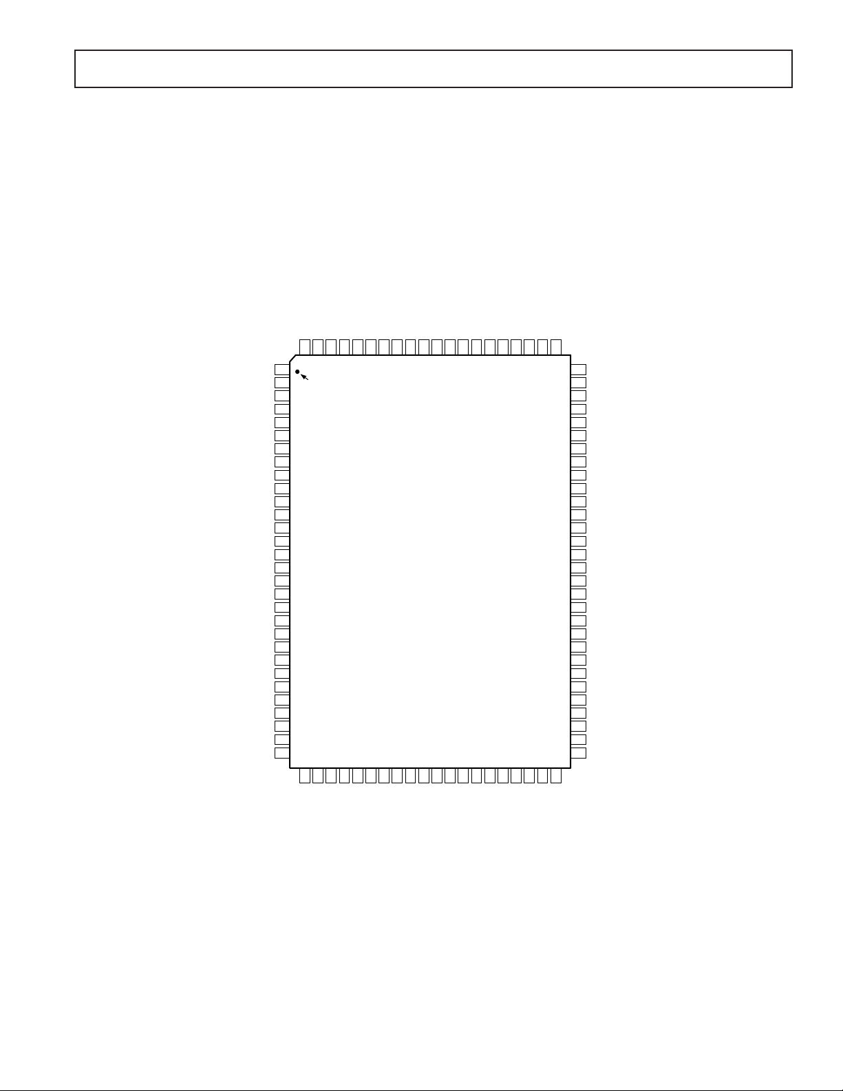
PIN CONFIGURATION
100-Lead PQFP
(S-100)
S1_BCLK/MDM_IRQ
S1_LRCLK/MDM_SEL/IRQ (12)/IRQ (13)
DD
SPORT_SCLK/LD_SEL/NC
GND
SPORT_SDFS/LD_DRQ/VOL_UP
SPORT_SDI/LD_IRQ/VOL_DN/GND
SPORT_SDO/LD_DACK/VOL_DN/GND
99989796959493929190898887868584838281
100
1
PIN 1
2
IDENTIFIER
3
4
5
6
7
8
9
10
11
12
13
14
15
16
17
18
19
20
21
22
23
DD
24
25
26
27
28
29
30
V
PC_D (0)
PC_D (2)
PC_D (1)
AD1816A
(Not to Scale)
GND
PC_D (3)
TOP VIEW
DD
V
PC_D (5)
PC_D (4)
PC_D (7)
PC_D (6)
S1_DATA/IRQ (3)/IRQ (9)
2
2
2
I
I
I
GND
80
IRQ (5)
79
IRQ (7)
78
IRQ (9)/IRQ (14)
77
IRQ (10)/IRQ (4)
76
IRQ (11)/IRQ (9)/IRQ (4)
75
IRQ (15)/IRQ (11)
74
DRQ (0)
73
DRQ (1)
72
DRQ (3)
71
V
DD
70
GND
69
XCTL1/RING/LD_SEL1
68
XCTL0/PCLKO/PNPRST
67
MIDI_OUT
66
MIDI_IN
65
GND
64
XTALO
63
XTALI
62
V
DD
61
DACK (0)
60
DACK (1)
59
DACK (3)
58
EE_CLK/GND
57
EE_DATA/GND
56
B_X
55
B_Y
54
A_X
53
A_Y
52
B_1
51
B_2
REV. A
NC = NO CONNECT
32
31
L_VID
R_VID
34
35
38
37
39
L_FILT
R_FILT
40
41
R_LINE
L_AAFILT
R_AAFILT
42
43
L_LINE
PHONE_IN
44
45
MIC
R_SYNTH
36
33
CC
REF
V
V
REF_X
GNDA
V
48
47
46
L_CD
R_CD
L_SYNTH
49
A_2
50
A_1
–9–

AD1816A
PIN CONFIGURATION
100-Lead TQFP
(ST-100)
2
I
S0_BCLK/GND
PC_A (15)
PC_A (14)
PC_A (13)
PC_A (12)
PC_A (11)
PC_A (10)
PC_A (9)
PC_A (8)
PC_A (7)
PC_A (6)
PC_A (5)
PC_A (4)
PC_A (3)
PC_A (2)
PC_A (1)
PC_A (0)
RESET
RX3D
CX3D
AEN
IOW
IOR
V
GND
S0_DATA/ VOL_UP
S0_LRCLK/ VOL_DN
2
2
I
SPORT_SDI/ LD_IRQ /VOL_DN /GND
I
SPORT_SDO/ LD_DACK / VOL_DN /GND
9998979695949392919089888786858483828180797877
100
1
PIN 1
2
IDENTIFIER
3
4
5
6
7
8
9
10
11
12
13
14
15
16
17
18
19
20
21
DD
22
23
24
25
27
28
29
26
R_VID
L_OUT
R_OUT
PHONE_OUT
SPORT_SCLK/LD_SEL /NC
SPORT_SDFS/ LD_DRQ /VOL_UP
30
31
CC
V
L_VID
V
GND
33
32
REF
V
GNDA
DD
PC_D (1)
PC_D (0)
34
35
REF_X
V
R_FILT
V
GND
PC_D (3)
PC_D (2)
AD1816A
TOP VIEW
(Not to Scale)
36
37
38
39
L_FILT
R_LINE
L_AAFILT
R_AAFILT
DD
PC_D (4)
40
L_LINE
PC_D (6)
PC_D (5)
PC_D (7)
41
42
43
MIC
R_SYNTH
PHONE_IN
S1_LRCLK/MDM_SEL/IRQ (12)/IRQ (13)
S1_DATA/IRQ (3)/IRQ (9)
S1_BCLK/MDM_IRQ
2
2
2
GND
I
I
I
44
45
46
47
A_2
L_CD
R_CD
L_SYNTH
IRQ (5)
IRQ (7)
48
49
A_1
B_2
IRQ (9)/IRQ (14)
76
75
IRQ (10)/IRQ (4)
74
IRQ (11)/IRQ (9)/IRQ (4)
73
IRQ (15)/IRQ (11)
72
DRQ (0)
71
DRQ (1)
DRQ (3)
70
69
V
DD
68
GND
67
XCTL1/RING/LD_SEL1
XCTL0/PCLKO/PNPRST
66
65
MIDI_OUT
64
MIDI_IN
63
GND
62
XTALO
61
XTALI
60
V
DD
59
DACK (0)
58
DACK (1)
57
DACK (3)
56
EE_CLK/GND
55
EE_DATA/GND
54
B_X
53
B_Y
52
A_X
51
A_Y
50
B_1
NC = NO CONNECT
–10–
REV. A

AD1816A
PIN FUNCTION DESCRIPTIONS
Analog Signals (All Inputs must be AC-Coupled)
Pin Name PQFP TQFP I/O Description
MIC 44 42 I Microphone Input. The MIC input may be either line-level or –20 dB from line-level (the
difference being made up through a software controlled 20 dB gain block). The mono MIC
input may be sent to the left and right channel of the ADC for conversion, or gained/
attenuated from +12 dB to –34.5 dB in 1.5 dB steps and then summed with left and right
line OUT before the Master Volume stage.
L_LINE 42 40 I Left Line-Level Input. The left line-level input may be sent to the left channel of the ADC;
gained/attenuated from +12 dB to –34.5 dB in 1.5 dB steps and then summed with left line
OUT (L_OUT).
R_LINE 41 39 I Right Line-Level Input. The right line-level input may be sent to the right channel of the
ADC; gained/attenuated from +12 dB to –34.5 dB in 1.5 dB steps and then summed with
right line OUT (R_OUT).
L_SYNTH 46 44 I Left Synthesizer Input. The left MIDI upgrade line-level input may be sent to the left
channel of the ADC; gained/attenuated from +12 dB to –34.5 dB in 1.5 dB steps and then
summed with left line OUT (L_OUT).
R_SYNTH 45 43 I Right Synthesizer Input. The right MIDI upgrade line-level input may be sent to the right
channel of the ADC; gained/attenuated from +12 dB to –34.5 dB in 1.5 dB steps and then
summed with right line OUT (R_OUT).
L_CD 48 46 I Left CD Line-Level Input. The left CD line-level input may be sent to the left channel of
the ADC; gained/attenuated from +12 dB to –34.5 dB in 1.5 dB steps and then summed
with left line OUT (L_OUT).
R_CD 47 45 I Right CD Line-Level Input. The right CD line-level input may be sent to the right channel
of the ADC; gained/attenuated from +12 dB to –34.5 dB in 1.5 dB steps and then summed
with right line OUT (R_OUT).
L_VID 32 30 I Left Video Input. The left audio track for a video line-level input may be sent to the left
channel of the ADC; gained/attenuated from +12 dB to –34.5 dB in 1.5 dB steps and then
summed with left line OUT (L_OUT).
R_VID 31 29 I Right Video Input. The right audio track for a video line-level input may be sent to the
right channel of the ADC; gained/attenuated from +12 dB to –34.5 dB in 1.5 dB steps and
then summed with right line OUT (R_OUT).
L_OUT 30 28 O Left Output. Left channel line-level post-mixed output. The final stage passes through the
Master Volume block and may be attenuated 0 dB to –45 dB in 1.5 dB steps.
R_OUT 29 27 O Right Output. Right channel line-level post-mixed output. The final stage passes through
the Master Volume block and may be attenuated 0 dB to –45 dB in 1.5 dB steps.
PHONE_IN 43 41 I Phone Input. Line-level input from a DAA/modem chipset.
PHONE_OUT 28 26 O Phone Output. Line-level output from a DAA/modem chipset.
RX3D 26 24 O Phat Stereo Phase Expander filter network, resistor pin.
CX3D 27 25 I Phat Stereo Phase Expander filter network, capacitor pin.
REV. A
–11–

AD1816A
Parallel Interface (All Outputs are 24 mA Drivers)
Pin Name PQFP TQFP I/O Description
PC_D[7:0] 85–88, 91–94 83–86, 89–92 I/O Bidirectional ISA Bus PC Data, 24 mA drive. Connects the AD1816A to
the low byte data on the bus.
IRQ (x)* 75–81, 83 73–79, 81 O Host Interrupt Request, 24 mA drive. IRQ (3)/IRQ (9), IRQ (5), IRQ (7),
IRQ (9)/IRQ (14), IRQ (10)/IRQ (4), IRQ (11)/IRQ (9)/IRQ (4), IRQ (12)/
IRQ (13), IRQ (15)/IRQ (11). Active HI signals indicating a pending interrupt.
DRQ (x) 72–74 70–72 O DMA Request, 24 mA drive. DRQ (0), DRQ (1), DRQ (3). Active HI sig-
nals indicating a request for DMA bus operation.
PC_A[15:0] 4–19 2–17 I ISA Bus PC Address. Connects the AD1816A to the ISA bus address lines.
AEN 20 18 I Address Enable. Low signal indicates a PIO transfer.
DACK (x) 59–61 57–59 I DMA Acknowledge. DACK (0), DACK (1), DACK (3). Active LO signal
indicating that a DMA operation can begin.
IOR 22 20 I I/O Read. Active LO signal indicates a read operation.
IOW 21 19 I I/O Write. Active HI signal indicates a write operation.
RESET 25 23 I Reset. Active HI.
Game Port
Pin Name PQFP TQFP I/O Description
A_1 50 48 I Game Port A, Button #1.
A_2 49 47 I Game Port A, Button #2.
A_X 54 52 I Game Port A, X-Axis.
A_Y 53 51 I Game Port A, Y-Axis.
B_1 52 50 I Game Port B, Button #1.
B_2 51 49 I Game Port B, Button #2.
B_X 56 54 I Game Port B, X-Axis.
B_Y 55 53 I Game Port B, Y-Axis.
MIDI Interface Signal (24 mA Drivers)
Pin Name PQFP TQFP I/O Description
MIDI_IN 66 64 I RXD MIDI Input. This pin is typically connected to Pin 15 of the game
port connector.
MIDI_OUT 67 65 O TXD MIDI Output. This pin is typically connected to Pin 12 of the game
port connector.
–12–
REV. A
Muxed Serial Ports (8 mA Drivers)
Pin Name PQFP TQFP I/O Description
2
I
S(0)_BCLK* 3 1 I I2S (0) Bit Clock.
2
I
S(0)_LRCLK* 2 100 I I2S (0) Left/Right Clock.
2
S(0)_DATA* 1 99 I I2S (0) Serial Data Input.
I
2
S(1)_BCLK* 82 80 I I2S (1) Bit Clock.
I
2
I
S(1)_LRCLK* 83 81 I I2S (1) Left/Right Clock.
2
S(1)_DATA* 81 79 I I2S (1) Serial Data Input.
I
SPORT_SDI* 100 98 I Serial Port Digital Serial Input.
SPORT_SCLK* 97 95 O Serial Port Serial Clock.
SPORT_SDFS* 98 96 O Serial Port Serial Data Frame Synchronization.
SPORT_SDO* 99 97 O Serial Port Serial Data Output.
Miscellaneous Analog Pins
Pin Name PQFP TQFP I/O Description
AD1816A
V
REF_X
V
REF
36 34 O Voltage Reference. Nominal 2.25 volt reference available for dc-coupling
and level-shifting. V
V
should be bypassed with 10 µF and 0.1 µF parallel capacitors.
REF_X
should not be used to sink or source signal current.
REF_X
35 33 I Voltage Reference Filter. Voltage reference filter point for external bypassing
only. V
should be bypassed with 10 µF and 0.1 µF parallel capacitors.
REF
L_FILT 38 36 I Left Channel Filter. Requires a 1.0 µF to analog ground for proper
operation.
R_FILT 37 35 I Right Channel Filter. Requires a 1.0 µF to analog ground for proper
operation.
L_AAFILT 40 38 I Left Channel Antialias Filter. This pin requires a 560 pF NPO
capacitor to analog ground for proper operation.
R_AAFILT 39 37 I Right Channel Antialias Filter. This pin requires a 560 pF NPO
capacitor to analog ground for proper operation.
Crystal Pin
Pin Name PQFP TQFP I/O Description
XTALO 64 62 O 33 MHz Crystal Output. If no Crystal is present leave XTALO
unconnected.
XTALI 63 61 I 33 MHz Clock. When using a crystal as a clock source, the crystal should
be connected between the XTALI and XTALO pins. Clock input may
be driven into XTALI in place of a crystal. When using an external clock,
V
must be 2.4 V rather than the VIH of 2.0 V specified for all other
IH
digital inputs.
External Logical Devices
Pin Name PQFP TQFP I/O Description
LD_IRQ* 100 98 I Logical Device IRQ.
LD_DACK* 99 97 O Logical Device DACK.
LD_DRQ* 98 96 I Logical Device DRQ.
LD_SEL* 97 95 O Logical Device Select.
MDM_SEL* 83 81 O Modem Chip Set Select.
MDM_IRQ* 82 82 I Modem Chip Set IRQ.
LD_SEL1* 69 67 O Logical Device (1) Select.
PNPRST* 68 66 O Plug and Play Reset.
REV. A
–13–
AD1816A
Hardware Volume Pins
Pin Name PQFP TQFP I/O Description
VOL_DN* 2, 99, 100 97, 98, 100 I Master Volume Down. Modifies output level on pins L_OUT and R_OUT.
When asserted LO, decreases Master Volume by 1.5 dB/sec. Must be asserted at
least 25 ms to be recognized. When asserted simultaneously with
put is muted. Output level modification reflected in indirect register [41].
VOL_UP* 1, 98 96, 99 I Master Volume Up. Modifies output level on pins L_OUT and R_OUT. When
asserted LO, increases Master Volume by 1.5 dB/sec. Must be asserted at least
25 ms to be recognized. When asserted simultaneously with
muted. Output level modification reflected in indirect register [41].
Control Pins
Pin Name PQFP TQFP I/O Description
XCTL0* 68 66 O External Control 0. The state of this pin (TTL HI or LO) is reflected in codec
indexed register. This pin is an open drain driver.
PCLKO* 68 66 O Programmable Clock Output. This pin can be programmed to generate an out-
put clock equal to F
, 8 × FS, 16 × FS, 32 × FS, 64 × FS, 128 × FS or 256 × FS.
S
MPEG decoders typically require a master clock of 256 × F
synchronization.
XCTL1* 69 67 O External Control 1. The state of this pin (TTL HI or LO) is reflected in codec
indexed register. Open drain, 8 mA active 0.5 mA pull-up resistor.
RING* 69 67 I Ring Indicator. Used to accept the ring indicator flag from the DAA.
VOL_UP, out-
VOL_UP, output is
for audio
S
Power Supplies
Pin Name PQFP TQFP I/O Description
V
CC
33 31 I Analog Supply Voltage (+5 V).
GNDA 34 32 I Analog Ground.
V
DD
23, 62, 71, 21, 60, 69, I Digital Supply Voltage (+5 V).
89, 95 87, 93
GND 3*, 24, 65, 1*, 22, 63, I Digital Ground.
70, 84, 90, 68, 82, 88,
96, 99*, 100* 94, 97*, 98*
Optional EEPROM Pins
Pin Name PQFP TQFP I/O Description
EE_CLK 58 56 O EEPROM Clock. Open drain output, requires external pull-up.
EE_DATA 57 55 I/O EEPROM Data. Open drain I/O, requires external pull-up.
*The position of this pin location/function is dependent on the EEPROM data.
–14–
REV. A

AD1816A
HOST INTERFACE
The AD1816A contains all necessary ISA bus interface logic on
chip. This logic includes address decoding for all onboard
resources, control and signal interpretation, DMA selection and
control logic, IRQ selection and control logic, and all interface
configuration logic.
The AD1816A supports a Type “F” DMA request/grant architecture for transferring data with the ISA bus through the 8-bit
interface. The AD1816A also supports DACK preemption. Programmed I/O (PIO) mode is also supported for control register
accesses and for applications lacking DMA control. The
AD1816A includes dual DMA count registers for full-duplex
operation enabling simultaneous capture and playback on separate DMA channels.
Codec Functional Description
The AD1816A’s full-duplex stereo codec supports business audio
and multimedia applications. The codec includes stereo audio
converters, complete on-chip filtering, MPC Level-2 and
Level-3 compliant analog mixing, programmable gain and attenuation, variable sample rate converters, extensive digital mixing
and FIFOs buffering the Plug and Play ISA bus interface.
Analog Inputs
The codec contains a stereo pair of ∑∆ analog-to-digital converters (ADC). Inputs to the ADC can be selected from the following analog signals: mono (PHONE_IN), mono microphone
(MIC), stereo line (LINE), external stereo synthesizer
(SYNTH), stereo CD ROM (CD), stereo audio from a video
source (VID) and post-mixed stereo or mono line output (OUT).
Analog Mixing
PHONE_IN, MIC, LINE, SYNTH, CD and VID can be mixed
in the analog domain with the stereo line OUT from the Σ∆
digital-to-analog converters (DAC). Each channel of the stereo
analog inputs can be independently gained or attenuated from
+12 dB to –34.5 dB in 1.5 dB steps, except for PHONE_IN,
which has a range of 0 dB to –45 dB steps. The summing path
for the mono inputs (MIC, and PHONE_IN to line OUT) duplicates mono channel data on both the left and right line OUT,
which can also be gained or attenuated from +12dB to –34.5 dB
in 1.5 dB steps for MIC, and +0 dB to –45.0 dB in 3 dB steps
for PHONE_IN. The left and right mono summing signals are
always identical being gained or attenuated equally.
Analog-to-Digital Datapath
The selector sends left and right channel information to the programmable gain amplifier (PGA). The PGA following the selector allows independent gain for each channel entering the ADC
from 0 dB to 22.5 dB in 1.5 dB steps.
For supporting time correlated I/O echo cancellation, the ADC
is capable of sampling microphone data on the left channel and
the mono summation of left and right OUT on the right channel.
The codec can operate in either a global stereo mode or a global
mono mode with left channel inputs appearing at both channels of
the 16-bit Σ∆ converters. Data can be sampled at the programmed
sampling frequency (from 4 kHz to 55.2 kHz with 1 Hz resolution).
Digital Mixing and Sample Rates
The audio ADC sample rate and the audio DAC sample rates
are completely independent. The AD1816A includes a variable
sample rate converter that lets the codec instantaneously change
and process sample rates from 4 kHz to 55.2 kHz with a resolution of 1 Hz. The in-band integrated noise and distortion
artifacts introduced by rate conversions are below –90 dB.
REV. A
–15–
Up to four channels of digital data can be summed together and
presented to the stereo DAC for conversion. Each digital channel pair can contain information encoded at a different sample
rate. For example, 8 kHz .wav data received from the ISA interface, 48 kHz MPEG audio data received from I
44.1 kHz CD data received from I
2
S(1) and internally generated
2
S(0), digital
22.05 kHz music data may be summed together and converted
by the DACs.
Digital-to-Analog Datapath
The internally generated music synthesizer data, PCM data
received from the ISA interface, data received from the I
port and data received from the I
2
S(1) port, and the DSP serial
2
S(0)
port passes through an attenuation mute stage. The attenuator
allows independent control over each digital channel, which can
be attenuated from 0 dB to –94.5 dB in 1.5 dB steps before being summed together and passed to the DAC, or the channel
may be muted entirely.
Analog Outputs and Phat Stereo
The analog output of the DAC can be summed with any of the
analog input signals. The summed analog signal enters the
Master Volume stage where each channel L_OUT, R_OUT and
PHONE_OUT may be attenuated from 0 dB to –46.5 dB in
1.5 dB steps or muted.
Analog Outputs and Phat Stereo
The AD1816A includes ADI’s proprietary Phat Stereo 3D
phase enhancement technology, which creates an increased
sense of spaciousness using two speakers. Our unique patented
feedback technology enables superior control over the width and
depth of the acoustic signals arriving at the human ear. The
AD1816A employs an electrical model of the speaker-to-ear
path allowing precise control over a signal’s phase at the ear. The
Phat Stereo circuitry expands apparent sound images beyond the
angle of the speakers by exploiting phase information in the audio
signal and creating a more immersive listening experience.
Digital Data Types
The codec can process 16-bit twos complement PCM linear
digital data, 8-bit unsigned magnitude PCM linear data and
8-bit µ-law or A-law companded digital data as specified in the
control registers. The AD1816A also supports ADPCM encoded in the Creative SoundBlaster ADPCM formats.
Host-Based Echo Cancellation Support
The AD1816A supports time correlated I/O data format by presenting MIC data on the left channel of the ADC and the mono
summation of left and right OUT on the right channel. The
ADC sample rates are independent of the DAC sample rate allowing the AD1816A to support ADC time correlated I/O data at
8 kHz and DAC data at any other sample rate in the range of
4 kHz to 55.2 kHz simultaneously.
Telephony Support
The AD1816A contains a PHONE_IN input and a
PHONE_OUT output. These pins are supplied so the AD1816A
may be connected to a modem chip set, a telephone handset or
down-line phone.
WSS and SoundBlaster Compatibility
Windows Sound System software audio compatibility is built
into the AD1816A.
SoundBlaster emulation is provided through the SoundBlaster
register set and the internal music synthesizer. SoundBlaster Pro
version 3.02 functions are supported, including record and Creative SoundBlaster ADPCM.

AD1816A
Virtually all applications developed for SoundBlaster, Windows
Sound System, AdLib and MIDI MPU-401 platforms run on the
AD1816A SoundPort Controller. Follow the same development
process for the controller as you would for these other devices.
As the AD1816A contains SoundBlaster (compatible) and
Windows Sound System logical devices. You may find the
following related development kits useful when developing
AD1816A applications.
Developer Kit for SoundBlaster Series, 2nd ed. © 1993,
Creative Labs, Inc., 1901 McCarthy Blvd., Milpitas, CA 95035
Microsoft Windows Sound System Driver Development Kit (CD),
Version 2.0, © 1993, Microsoft Corp., One Microsoft Way,
Redmond, WA 98052
The following reference texts can serve as additional sources of information on developing applications that run on the AD1816A.
S. De Furia & J. Scacciaferro, The MIDI Implementation Book,
(© 1986, Third Earth, Pompton Lake)
C. Petzold, Programming Windows: the Microsoft guide to writ-
ing applications for Windows 3.1, 3rd. ed., (© 1992, Microsoft
Press, Redmond)
K. Pohlmann, Principles of Digital Audio, (© 1989, Sams,
Indianapolis)
A. Stolz, The SoundBlaster Book, (© 1993, Abacaus, Grand
Rapids)
J. Strawn, Digital Audio Engineering, An Anthology, (© 1985,
Kaufmann, Los Altos)
Yamamoto, MIDI Guidebook, 4th. ed., (© 1987, 1989,
Roland Corp.)
Multimedia PC Capabilities
The AD1816A is MPC-2 and MPC-3 compliant. This compliance is achieved through the AD1816A’s flexible mixer and the
embedded chip resources.
Music Synthesis
The AD1816A includes an embedded music synthesizer that
emulates industry standard OPL3 FM synthesizer chips and
delivers 20 voice polyphony. The internal synthesizer generates
digital music data at 22.05 kHz and is summed into the DACs
digital data stream prior to conversion. To sum synthesizer data
with the ADC output, the ADC must be programmed for a
22.05 kHz sample rate.
The synthesizer is a hardware
implementation of Eusynth-1+
code that was developed by
EUP
HONICS
Euphonics, a research and development company that specializes
in audio processing and electronic
music synthesis.
EuSynth-1+
Wavetable MIDI Inputs
The AD1816A has a dedicated analog input for receiving an
analog wavetable synthesizer output. Alternatively, a wavetable
synthesizer’s I
nected to one of the AD1816A’s I
table data from the AD1816A’s I
other digital data streams being handled by the AD1816A and
then sent to the 16-bit Σ∆ DAC.
2
S formatted digital output can be directly con-
2
S serial ports. Digital wave-
2
S port may be summed with
MIDI
The primary interface for communicating MIDI data to and from
the host PC is the compatible MPU-401 interface that operates
only in UART mode. The MPU-401 interface has two built-in
FIFOs: a 64-byte receive FIFO and a 16-byte transmit FIFO.
Game Port
An IBM-compatible game port interface is provided on chip.
The game port supports up to two joysticks via a 15-pin D-sub
connector. Joystick registers supporting the Microsoft Direct
Input standard are included as part of the codec register map.
The AD1816A may be programmed to automatically sample the
game port and save the value in the Joystick Position Data Register. When enabled, this feature saves up to 10% CPU MIPS
by off-loading the host from constantly polling the joystick port.
Volume Control
The registers that control the Master Volume output stage are
accessible through the ISA Bus. Master Volume output can also
be controlled through a 2-pin hardware interface. One pin is
used to increase the gain, the other pin attenuates the output
and both pins together entirely mute the output. Once muted, any
further activity on these pins will unmute the AD1816A’s output.
Plug and Play Configuration
The AD1816A is fully Plug and Play configurable. For motherboard applications, the built-in Plug and Play protocol can be
disabled with a software key providing a back door for the BIOS
to configure the AD1816A’s logical devices. For information on
the Plug and Play mode configuration process, see the Plug and
Play ISA Specification Version 1.0a (May 5, 1994). All the
AD1816A’s logical devices comply with Plug and Play resource
definitions described in the specification.
The AD1816A may alternatively be configured using an optional
Plug and Play Resource ROM. When the EEPROM is present,
some additional AD1816A muxed-pin features become available. For example, pins that control an external modem logical
device are muxed with the DSP serial port. Some of these pin
option combinations are mutually exclusive (see Appendix A for
more information).
REFERENCES
The AD1816A also complies with the following related specifications; they can be used as an additional reference to AD1816A
operations beyond the material in this data sheet.
Plug and Play ISA Specification, Version 1.0a, © 1993, 1994,
Intel Corp. & Microsoft Corp., One Microsoft Way,
Redmond, WA 98052
Multimedia PC Level 2 Specification, © 1993, Multimedia PC
Marketing Council, 1730 M St. NW, Suite 707, Washington,
DC 20036
MIDI 1.0 Detailed Specification & Standard MIDI Files 1.0,
© 1994, MIDI Manufacturers Association, PO Box 3173
La Habra, CA 90632-3173
Recommendation G.711-Pulse Code Modulation (PCM) Of Voice
Frequencies (µ-Law & A-Law Companding), The International
Telegraph and Telephone Consultative Committee IX Plenary
Assembly Blue Book, Volume III - Fascicle III.4, General
Aspects Of Digital Transmission Systems; Terminal
Equipment’s, Recommendations G.700 - G.795, (Geneva,
1988), ISBN 92-61-03341-5
–16–
REV. A
 Loading...