


UCC561
Low Voltage Differential SCSI (LVD) 27 Line Regulator Set
FEATURES
∙SCSI SPI-2 LVD SCSI 27 Line Low Voltage Differential Regulator
∙2.7V to 5.25V Operation
∙Integrated Regulator Set for LVD SCSI
∙Differential Failsafe Bias
BLOCK DIAGRAM
DESCRIPTION
The UCC561 LVD Regulator set is designed to provide the correct references voltages and bias currents for LVD termination resistor networks (475 , 121
, 121 and 475
 ). The device also provides a 1.3V output for Diff Sense signaling. With the proper resistor network, the UCC561 solution will meet the common mode bias impedance, differential bias, and termination impedance requirements of SPI-2 (Ultra2) and SPI-3 (Ultra3).
This device incorporates into a single monolith, two sink/source reference voltage regulators, a 1.3V buffered output and protection features. The protection features include thermal shut down and active current limiting circuitry. The UCC561 is offered in 16-pin SOIC(DP) package.
|
|
|
|
|
|
|
|
|
|
|
|
|
|
|
|
|
|
|
|
|
|
|
|
|
|
|
REF 1.3V |
|
|
|
7 |
DIFSENS |
|
|
|
|
|
|
|
|
|
|
|
|
||||||
|
|
|
|
|
|
|
|
|
|
|
|
|
1.3V +/– 0.1V |
|
|
|
|
|
|
|
|
|
|
|
|
|
|
|
|
|
|
|
|
TRMPWR |
2 |
|
|
|
|
|
|
|
|
|
|
|
|
|
||
|
|
|
||||||||||||||
|
|
|
|
|
|
|
|
|
|
|
|
|
|
|
|
|
2.7V < 5.25V |
|
|
|
|
|
|
|
|
|
|
|
|
|
|
|
|
|
|
|
|
|
|
|
|
|
|
REF 1.75V |
|
|
|
6 |
REG1 |
|
|
|
|
|
|
|
|
|
|
|
|
||||||
|
|
|
|
|
|
|
|
|
|
|
|
|
|
|
|
|
|
|
|
|
|
|
|
|
|
|
1.75V +/–50mV |
|
|
|
|||
|
|
|
|
|
|
|
|
|
|
|
|
|
||||
|
|
|
|
|||||||||||||
|
|
|
|
|
|
|
|
|
|
200mA SOURCE/SINK |
|
|
|
|||
|
|
|
|
|||||||||||||
|
|
|
|
|
|
|||||||||||
|
|
|
|
|
|
|
|
|
|
|
|
SOURCE/SINK REGULATOR |
|
|
|
|
|
|
|
|
|
|
|
|
|
|
|
|
|
|
|
||
|
|
|
|
|
|
|
|
|
|
|
|
|
|
|
||
|
|
|
|
|
|
|
|
|
|
|
|
|
|
|
||
|
|
|
|
|
|
|
|
|
|
|
|
|
|
|
||
|
|
|
|
|
|
|||||||||||
|
|
|
|
|||||||||||||
|
|
|
|
|
|
|
|
|
|
REF 0.75V |
|
|
|
3 |
REG2 |
|
|
|
|
||||||||||||||
|
|
|
|
|
|
|
|
|
|
|
|
|
|
|
|
|
|
|
|
|
|
|
|
|
|
|
0.75V +/–50mV |
|
|
|
|||
|
|
|
|
|
|
|||||||||||
|
|
|
|
|
|
|
|
|
|
200mA SOURCE/SINK |
|
|
|
|||
|
|
|
|
|
|
|
|
|
|
|
|
|
||||
|
|
|
|
|
|
|
|
|
|
|
|
|
|
|
|
|
|
|
|
|
|
|
|
|
|
|
|
|
|
|
|
|
|
|
|
|
|
|
|
|
|
|
|
|
|
|
|
|
|
|
4
PGND
UDG-98093
SLUS413 - MAY 1999
ABSOLUTE MAXIMUM RATINGS
TERMPWR . . . . . . . . . . . . . . . . . . . . . . . . . . . . . . . . . . . . . +6V Package Dissipation . . . . . . . . . . . . . . . . . . . . . . . . . . . . . 1.2W Junction Temperature. . . . . . . . . . . . . . . . . . . –55°C to +150°C Storage Temperature . . . . . . . . . . . . . . . . . . . –65°C to +150°C
Currents are positive into, negative out of the specified terminal. Consult Packaging Section of Databook for thermal limitations and considerations of packages.
RECOMMENDED OPERATING CONDITIONS
TERMPWR Voltage . . . . . . . . . . . . . . . . . . . . . . . 2.7V to 5.25V
UCC561
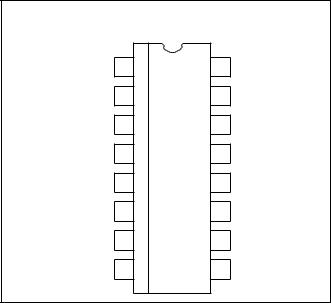
CONNECTION DIAGRAMS
SOIC-16 (TOP VIEW)
DP Packages
N/C |
1 |
16 |
N/C |
TERMPWR |
2 |
15 |
N/C |
REG2 |
3 |
14 |
N/C |
HSPGND |
4 |
13 |
HSGND |
HSGND |
5 |
12 |
HSGND |
REG1 |
6 |
11 |
N/C |
DIFSENS |
7 |
10 |
N/C |
N/C |
8 |
9 |
N/C |
ELECTRICAL CHARACTERISTICS: Unless otherwise specified these specifications apply for TA = 0°C to 70°C, TERMPWR = 3.3V.
|
PARAMETER |
TEST CONDITIONS |
MIN |
TYP |
MAX |
UNITS |
TERMPWR Supply Current Section |
|
|
|
|
|
|
TERMPWR Supply Current |
No Load |
|
|
40.0 |
mA |
|
TERMPWR Voltage |
|
2.7 |
|
5.25 |
V |
|
Regulator Section |
|
|
|
|
|
|
1.75 |
Volt Regulator |
REG1 (± 125mA) |
1.7 |
1.75 |
1.8 |
V |
1.3 Volt Regulator |
DIFSENS , No Load |
1.2 |
1.3 |
1.4 |
V |
|
0.75 |
Volt Regulator |
REG2 (± 125mA) |
0.7 |
0.75 |
0.8 |
V |
1.75 |
Volt Regulator Source Current |
VO = 1.25 |
|
|
–200 |
mA |
1.75 |
Volt Regulator Sink Current |
VO = 2.25 |
200 |
|
|
mA |
1.75 |
Volt Sink Current Limit |
|
|
|
700 |
mA |
1.75 |
Volt Source Current Limit |
|
–700 |
|
|
mA |
1.3 Volt Regulator Source Current |
DIFSENS, GND |
–5 |
|
–15 |
mA |
|
1.3 Volt Regulator Sink Current |
DIFSENS, 2.4V |
50 |
|
200 |
μA |
|
0.75 |
Volt Regulator Source Current |
VO = 0.25 |
|
|
–200 |
mA |
0.75 |
Volt Regulator Sink Current |
VO = 1.25 |
200 |
|
|
mA |
0.75 |
Source Current Limit |
|
|
|
700 |
mA |
0.75 |
Sink Current Limit |
|
–700 |
|
|
mA |
Note 1: Guaranted by design. Not 100% tested in production.
2
 Loading...