


UCC5618QPTR
Texas Instruments UCC5618QPTR, UCC5618QP, UCC5618PWPTR, UCC5618PWP, UCC5618DWPTR Datasheet
...
UCC5618
DESCRIPTION
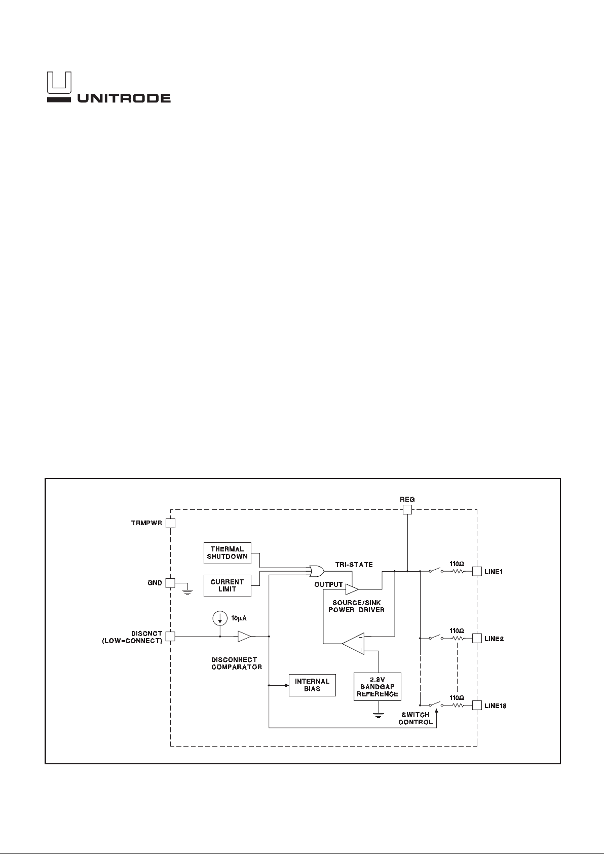
The UCC5618 provides 18 lines of active termination for a SCSI (Small
Computers Systems Interface) parallel bus. The SCSI standard recommends and Fast-20 (Ultra) requires active termination at both ends of the
cable.
Pin for pin compatible with the UC5601 and UC5608, the UCC5618 is ideal
for high performance 5V SCSI systems, Termpwr 4.0-5.25V. During disconnect the supply current is only 50µA typical, which makes the IC attractive
for lower powered systems.
The UCC5618 is designed with a low channel capacitance of 2pF, which
eliminates effects on signal integrity from disconnected terminators at interim points on the bus.
The power amplifier output stage allows the UCC5618 to source full termination current and sink active negation current when all termination lines
are actively negated.
The UCC5618, as with all Unitrode terminators, is completely hot pluggable
and appears as high impedance at the terminating channels with
TRMPWR=0V or open.
Internal circuit trimming is utilized, first to trim the 110Ω impedance, and
then most importantly, to trim the output current as close to the max
SCSI-3 spec as possible, which maximizes noise margin in fast SCSI operation.
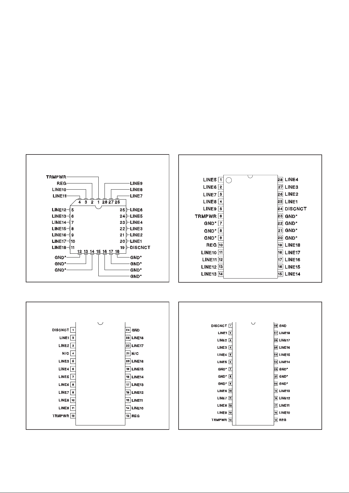
This device is offered in low thermal resistance versions of the industry
standard 28 pin wide body SOIC, TSSOP and PLCC.
18-Line SCSI Terminator
FEATURES
• Complies with SCSI, SCSI-2, SCSI-3,
SPI and FAST-20 Standards
• 2pF Channel Capacitance During
Disconnect
• 50µA Supply Current in Disconnect
Mode
• 110Ω Termination
• SCSI Hot Plugging Compliant, 10nA
Typical
• +400mA Sinking Current for Active
Negation
• –650mA Sourcing Current for
Termination
• Trimmed Impedance to 5%
• Thermal Shutdown
• Current Limit
6/98
BLOCK DIAGRAM
UDG-96005-1
Patented Circuit Design
2
UCC5618
PLCC-28 (Top View)
QP Package
ABSOLUTE MAXIMUM RATINGS
TEMPWR.......................................+7V
Signal Line Voltage ..........................0Vto+7V
Regulator Output Current ...........................1A
Storage Temperature ...................–65°C to +150°C
Operating Junction Temperature ..........–55°C to +150°C
Lead Temperature (Soldering, 10 Seconds) ..........300°C
All currents are positive into, negative out of the specified
terminal. Consult Packaging Section of Databook for thermal
limitations and considerations of packages.
CONNECTION DIAGRAMS
* DWP package pins 12–18 serve as both heatsink and signal
ground.
* PWP package pin 23 serves as signal ground; pins 7, 8, 9,
20, 21, and 22 serve as heatsink ground.
TSSOP-28 (Top View)
PWP Package
Note: Drawings are not to scale.
DIL-24 (Top View)
N Package
* DWP package pin 28 serves as signal ground; pins 7, 8, 9,
20, 21, 22 serve as heatsink/ground.
SOIC-28 (Top View)
DWP Package
 Loading...