


THS6002
DUAL DIFFERENTIAL LINE DRIVERS AND RECEIVERS
SLOS202D± JANUARY 1998± REVISED JULY 1999
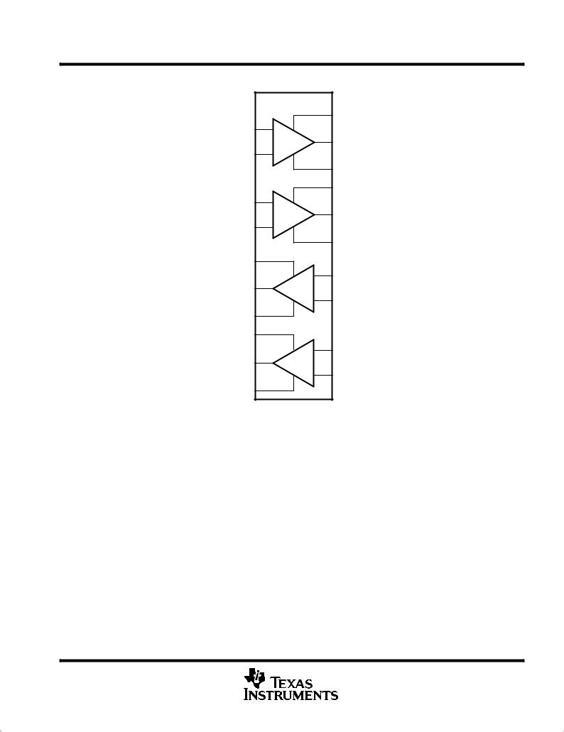
D |
ADSL Differential Line Driver and Receiver |
DWP PACKAGE |
D |
Driver Features |
(TOP VIEW) |
|
|
± 140 MHz Bandwidth (±3dB) With |
VCC ± |
1 |
20 |
VCC ± |
||
|
25-Ω Load |
|
|
||||
|
D1 OUT |
2 |
19 |
D2 OUT |
|||
|
± 315 MHz Bandwidth (±3dB) With |
VCC+ |
3 |
18 |
VCC+ |
||
|
100-Ω Load |
D1 IN+ |
4 |
17 |
D2 IN+ |
||
|
± 1000 V/µs Slew Rate, G = 2 |
D1 IN± |
5 |
16 |
D2 IN± |
||
|
± 400 mA Output Current Minimum Into |
R1 IN± |
6 |
15 |
R2 IN± |
||
|
25-Ω Load |
R1 IN+ |
7 |
14 |
R2 IN+ |
||
|
± ±72 dB 3rd Order Harmonic Distortion at |
VCC+ |
8 |
13 |
VCC+ |
||
|
f = 1 MHz, 25-Ω Load, and 20 VO(PP) |
R1 OUT |
9 |
12 |
R2 OUT |
||
|
VCC ± |
||||||
D |
Receiver Features |
10 |
11 |
V |
CC |
± |
|
|
|
|
|
|
|||
|
± 330 MHz Bandwidth (±3dB) |
|
|
|
|
|
|
|
± 900 V/µs Slew Rate at G = 2 |
|
|
|
|
|
|
± ±76 dB 3rd Order Harmonic Distortion at f = 1 MHz, 150-Ω Load, and 20 VO(PP)
DWide Supply Range ±4.5 V to ±16 V
Cross Section View Showing PowerPAD
D Available in the PowerPAD Package
D Improved Replacement for AD816 or
EL1501
D Evaluation Module Available
description
The THS6002 contains two high-current, high-speed drivers and two high-speed receivers. These drivers and receivers can be configured differentially for driving and receiving signals over low-impedance lines. The THS6002 is ideally suited for asymmetrical digital subscriber line (ADSL) applications where it supports the high-peak voltage and current requirements of that application. Both the drivers and the receivers are current feedback amplifiers designed for the high slew rates necessary to support low total harmonic distortion (THD) in ADSL applications. Separate power supply connections for each driver are provided to minimize crosstalk.
HIGH-SPEED xDSL LINE DRIVER/RECEIVER FAMILY
|
|
|
|
|
|
BW |
SR |
THD |
IO |
Vn |
|||
DEVICE |
DRIVER |
RECEIVER |
5 V |
±5 V |
±15 V |
f = 1 MHz |
|||||||
(MHz) |
(V/ s) |
(mA) |
|
|
|
||||||||
(nV/√ Hz) |
|||||||||||||
|
|
|
|
|
|
(dB) |
|||||||
|
|
|
|
|
|
|
|
|
|
|
|
||
|
|
|
|
|
|
|
|
|
|
|
|
||
THS6002 |
• |
• |
|
• |
• |
140 |
1000 |
±62 |
500 |
1.7 |
|
||
THS6012 |
• |
|
|
• |
• |
140 |
1300 |
±65 |
500 |
1.7 |
|
||
THS6022 |
• |
|
|
• |
• |
210 |
1900 |
±66 |
250 |
1.7 |
|
||
THS6062 |
|
• |
• |
• |
• |
100 |
100 |
±72 |
90 |
1.6 |
|
||
THS7002 |
|
• |
|
• |
• |
70 |
100 |
±84 |
25 |
2.0 |
|
||
CAUTION: The THS6002 provides ESD protection circuitry. However, permanent damage can still occur if this device is subjected to high-energy electrostatic discharges. Proper ESD precautions are recommended to avoid any performance degradation or loss of functionality.
Please be aware that an important notice concerning availability, standard warranty, and use in critical applications of Texas Instruments semiconductor products and disclaimers thereto appears at the end of this data sheet.
PowerPAD is a trademark of Texas Instruments Incorporated.
PRODUCTION DATA information is current as of publication date. Products conform to specifications per the terms of Texas Instruments standard warranty. Production processing does not necessarily include testing of all parameters.
Copyright 1999, Texas Instruments Incorporated
POST OFFICE BOX 655303 •DALLAS, TEXAS 75265 |
1 |

THS6002
DUAL DIFFERENTIAL LINE DRIVERS AND RECEIVERS
SLOS202D± JANUARY 1998± REVISED JULY 1999
description (continued)
The THS6002 is packaged in the patented PowerPAD package. This package provides outstanding thermal characteristics in a small footprint package, which is fully compatible with automated surface mount assembly procedures. The exposed thermal pad on the underside of the package is in direct contact with the die. By simply soldering the pad to the PWB copper and using other thermal outlets, the heat is conducted away from the junction.
|
AVAILABLE OPTIONS |
|
|
|
PACKAGED DEVICE |
||
|
|
|
|
TA |
PowerPAD PLASTIC |
EVALUATION |
|
SMALL OUTLINE² |
|||
|
MODULE |
||
|
(DWP) |
||
|
|
||
|
|
|
|
0°C to 70°C |
THS6002CDWP |
THS6002EVM |
|
|
|
|
|
± 40°C to 85°C |
THS6002IDWP |
|
|
²The DWP packages are available taped and reeled. Add an R suffix to the device type (i.e., THS6002CDWPR)
absolute maximum ratings over operating free-air temperature (unless otherwise noted)²
Supply voltage, VCC+ to VCC± . . . . . . . . . . . . . . . . . . . . . . . . . . . . . . . . . . . . . . . . . . . . . . . . . . . . . |
. . . . . . . . . . 33 V |
Input voltage, VI (driver and receiver) . . . . . . . . . . . . . . . . . . . . . . . . . . . . . . . . . . . . . . . . . . . . . . . . |
. . . . . . . . ± VCC |
Output current, IO (driver) (see Note 1) . . . . . . . . . . . . . . . . . . . . . . . . . . . . . . . . . . . . . . . . . . . . . . . |
. . . . . . 800 mA |
Output current, IO (receiver) (see Note 1) . . . . . . . . . . . . . . . . . . . . . . . . . . . . . . . . . . . . . . . . . . . . . |
. . . . . . 150 mA |
Differential input voltage, VID (driver and receiver) . . . . . . . . . . . . . . . . . . . . . . . . . . . . . . . . . . . . . |
. . . . . . . . . . 6 V |
Continuous total power dissipation at (or below) TA = 25°C (see Note 1) . . . . . . . . . . . . . . . . . . |
. . . . . . . . 5.8 W |
Operating free air temperature, TA . . . . . . . . . . . . . . . . . . . . . . . . . . . . . . . . . . . . . . . . . . . . . . . . . . . |
±40°C to 85°C |
Storage temperature, Tstg . . . . . . . . . . . . . . . . . . . . . . . . . . . . . . . . . . . . . . . . . . . . . . . . . . . . . . . . . |
±65°C to 125°C |
Lead temperature, 1,6 mm (1/16 inch) from case for 10 seconds . . . . . . . . . . . . . . . . . . . . . . . . |
. . . . . . . 300°C |
² Stresses beyond those listed under ªabsolute maximum ratingsº may cause permanent damage to the device. These are stress ratings only, and functional operation of the device at these or any other conditions beyond those indicated under ªrecommended operating conditionsº is not implied. Exposure to absolute-maximum-rated conditions for extended periods may affect device reliability.
NOTE 1: The THS6002 incorporates a PowerPad on the underside of the chip. This acts as a heatsink and must be connected to a thermal dissipation plane for proper power dissipation. Failure to do so can result in exceeding the maximum junction temperature, which could permanently damage the device. See the Thermal Information section of this document for more information about PowerPad technology.
recommended operating conditions
|
|
MIN |
TYP |
MAX |
UNIT |
|
|
|
|
|
|
Supply voltage, VCC+ and VCC ± |
Split supply |
± 4.5 |
|
± 16 |
V |
|
|
|
|
||
Single supply |
9 |
|
32 |
||
|
|
|
|||
|
|
|
|
|
|
Operating free-air temperature, TA |
C suffix |
0 |
|
70 |
°C |
|
|
|
|
||
I suffix |
± 40 |
|
85 |
||
|
|
|
|||
|
|
|
|
|
|
2 |
POST OFFICE BOX 655303 •DALLAS, TEXAS 75265 |
THS6002
DUAL DIFFERENTIAL LINE DRIVERS AND RECEIVERS
SLOS202D± JANUARY 1998± REVISED JULY 1999
functional block diagram
|
|
|
|
Driver 1 |
|
|
|
|
|
|
|
3 |
VCC+ |
D1 IN+ |
4 |
+ |
2 |
|
||
|
|
|
5 |
|
D1 OUT |
|
D1 IN± |
_ |
|
|
|||
|
|
|
|
|||
|
|
|
|
|
1 |
VCC± |
|
|
|
|
Driver 2 |
|
|
|
|
|
|
18 |
|
|
|
|
|
17 |
|
VCC+ |
|
D2 IN+ |
+ |
19 |
|
|||
|
|
|
16 |
|
D2 OUT |
|
D2 IN± |
_ |
|
|
|||
|
|
|
||||
|
|
|
|
|||
|
|
|
|
Receiver 1 |
20 |
VCC± |
|
|
|
8 |
|
|
|
V |
CC |
+ |
|
|
|
|
|
|
|
|
7 |
|
|
|
|
|
|
+ |
R1 IN+ |
|
R1 OUT 9 |
|
|||||
|
|
|
||||
|
|
|
|
_ |
6 |
R1 IN± |
VCC± |
10 |
Receiver 2 |
|
|
||
|
|
|
13 |
|
|
|
VCC+ |
|
|
|
|||
|
|
14 |
|
|||
|
|
|
|
+ |
R2 IN+ |
|
|
|
|
12 |
|
||
R2 OUT |
|
15 |
|
|||
|
|
|
|
_ |
R2 IN± |
|
VCC± |
11 |
|
|
|
||
POST OFFICE BOX 655303 •DALLAS, TEXAS 75265 |
3 |
THS6002
DUAL DIFFERENTIAL LINE DRIVERS AND RECEIVERS
SLOS202D± JANUARY 1998± REVISED JULY 1999
DRIVER
electrical characteristics, VCC = ±15 V, RL = 25 Ω, RF = 1 kΩ, TA = 25°C (unless otherwise noted)
|
PARAMETER |
|
|
|
|
|
TEST CONDITIONS² |
MIN |
TYP |
MAX |
UNIT |
|||
VCC |
Power supply operating range |
Split supply |
|
|
|
±4.5 |
|
±16.5 |
V |
|||||
|
|
|
|
|
|
|
|
|
|
|
||||
Single supply |
|
|
|
9 |
|
33 |
||||||||
|
|
|
|
|
|
|
|
|||||||
|
|
|
|
|
|
|
|
|
|
|
|
|
|
|
|
|
|
|
|
|
|
|
|
|
|
3 |
3.2 |
|
|
|
|
|
|
|
|
|
|
|
|
VCC = ± 5 V |
to |
to |
|
|
|
|
Single ended |
RL = 25 Ω |
|
|
|
± 2.8 |
± 3 |
|
V |
||||
|
|
|
|
|
|
|
|
|||||||
|
|
|
|
|
11.8 |
12.5 |
|
|||||||
|
|
|
|
|
|
|
|
|
|
|
|
|
||
|
|
|
|
|
|
|
|
|
|
VCC = ± 15 V |
to |
to |
|
|
VO |
Output voltage swing |
|
|
|
|
|
|
|
|
|
±11.5 |
±12.2 |
|
|
|
|
|
|
|
|
|
|
|
|
|
|
|
||
|
|
|
|
|
|
|
|
|
6 |
6.4 |
|
|
||
|
|
|
|
|
|
|
|
|
|
|
|
|
||
|
|
|
|
|
|
|
|
|
|
VCC = ± 5 V |
to |
to |
|
|
|
|
Differential |
RL = 50 Ω |
|
|
|
± 5.6 |
± 6 |
|
V |
||||
|
|
|
|
|
23.6 |
25 |
|
|||||||
|
|
|
|
|
|
|
|
|
|
|
|
|
||
|
|
|
|
|
|
|
|
|
|
VCC = ± 15 V |
to |
to |
|
|
|
|
|
|
|
|
|
|
|
|
|
± 23 |
± 24.4 |
|
|
|
|
|
|
|
|
|
|
|
|
|
|
|||
VICR |
Common-mode input voltage range |
VCC = ± |
5 V |
|
|
|
± 3.6 |
± 3.7 |
|
V |
||||
VCC = ± |
15 V |
|
|
|
± 13.4 |
± 13.5 |
|
|||||||
|
|
|
|
|
|
|
|
|||||||
VIO |
Input offset voltage |
|
VCC = ± |
5 V or ± 15 V |
TA = 25°C |
|
2 |
5 |
mV |
|||||
|
TA = full range |
|
|
7 |
||||||||||
|
|
|
|
|
|
|
|
|
|
|
|
|
||
|
Input offset voltage drift |
|
VCC = ± |
5 V or ± 15 V, |
TA = full range |
|
|
20 |
µV/°C |
|||||
|
Differential input offset voltage |
VCC = ± |
5 V or ± 15 V |
TA = 25°C |
|
1.5 |
4 |
mV |
||||||
|
TA = full range |
|
|
5 |
||||||||||
|
|
|
|
|
|
|
|
|
|
|
|
|
||
|
Differential input offset voltage drift |
VCC = ± |
5 V or ± 15 V, |
TA = full range |
|
|
10 |
µV/°C |
||||||
|
|
|
|
|
|
|
|
|
|
TA = 25°C |
|
3 |
9 |
|
|
|
Negative |
|
|
|
|
|
|
|
TA = full range |
|
|
12 |
A |
|
|
|
|
|
|
|
|
|
|
|
|
|
||
|
|
|
|
|
|
± |
|
± |
|
TA = 25°C |
|
4 |
10 |
|
IIB |
Input bias current |
Positive |
VCC = |
|
5 V or |
|
15 V |
TA = full range |
|
|
12 |
A |
||
|
|
|
|
|
|
|
|
|
|
|
|
|
||
|
|
|
|
|
|
|
|
|
|
TA = 25°C |
|
1.5 |
8 |
|
|
|
Differential |
|
|
|
|
|
|
|
TA = full range |
|
|
11 |
A |
|
|
|
|
|
|
|
|
|
|
|
|
|
||
IO |
Output current (see Note 2) |
|
VCC = ± |
5 V, |
|
|
RL = 5 Ω |
|
500 |
|
mA |
|||
|
VCC = ± |
15 V, |
|
|
RL = 25 Ω |
400 |
500 |
|
||||||
|
|
|
|
|
|
|
||||||||
IOS |
Short-circuit output current (see Note 2) |
|
|
|
|
|
|
|
|
|
800 |
|
mA |
|
|
Open loop transresistance |
|
VCC = ± |
5 V |
|
|
|
|
1.5 |
|
MΩ |
|||
|
|
VCC = ± |
15 V |
|
|
|
|
5 |
|
|||||
|
|
|
|
|
|
|
|
|
||||||
CMRR |
Common-mode rejection ratio |
V |
CC |
= ± |
5 V or ± 15 V, |
T = full range |
62 |
70 |
|
dB |
||||
|
|
|
|
|
||||||||||
|
|
|
|
|
||||||||||
|
Differential common-mode rejection ratio |
|
|
|
|
|
|
A |
|
100 |
|
|
||
|
|
|
|
|
|
|
|
|
|
|
|
|||
|
|
|
|
|
|
|
|
|
|
|
||||
|
Crosstalk |
Driver to driver |
VI = 200 mV, |
|
|
f = 1 MHz |
|
± 62 |
|
dB |
||||
² Full range is 0°C to 70°C for the THS6002C and ± 40°C to 85°C for the THS6002I.
NOTE 2: A heat sink is required to keep the junction temperature below absolute maximum when an output is heavily loaded or shorted. See absolute maximum ratings and Thermal Information section.
4 |
POST OFFICE BOX 655303 •DALLAS, TEXAS 75265 |
THS6002
DUAL DIFFERENTIAL LINE DRIVERS AND RECEIVERS
SLOS202D± JANUARY 1998± REVISED JULY 1999
DRIVER
electrical characteristics, VCC = ±15 V, RL = 25 Ω, RF = 1 kΩ, TA = 25°C (unless otherwise noted)
(continued)
|
PARAMETER |
|
TEST CONDITIONS² |
MIN |
TYP |
MAX |
UNIT |
|
|
|
V = ± 5 V |
TA = 25°C |
± 68 |
± 74 |
|
dB |
|
|
|
|
|
|
|
|||
|
|
CC |
|
TA = full range |
± 65 |
|
|
|
PSRR |
Power supply rejection ratio |
|
|
|
|
|
||
VCC |
= ± 15 V |
TA = 25°C |
± 64 |
± 72 |
|
dB |
||
|
|
|
||||||
|
|
TA = full range |
± 62 |
|
|
|||
|
|
|
|
|
|
|
||
CI |
Differential input capacitance |
|
|
|
|
1.4 |
|
pF |
RI |
Input resistance |
|
|
|
|
300 |
|
kΩ |
RO |
Output resistance |
Open loop |
|
|
13 |
|
Ω |
|
|
|
VCC |
= ± 5 V |
TA = 25°C |
|
8.5 |
10 |
|
ICC |
Quiescent current |
TA = full range |
|
|
12 |
mA |
||
|
|
|
|
|||||
VCC |
= ± 15 V |
TA = 25°C |
|
11.5 |
13 |
|||
|
|
|
|
|||||
|
|
TA = full range |
|
|
15 |
|
||
|
|
|
|
|
|
|
||
² Full range is 0°C to 70°C for the THS6002C and ± 40°C to 85°C for the THS6002I.
operating characteristics, VCC = ±15 V, RL = 25 Ω, RF = 1 kΩ, TA = 25°C (unless otherwise noted)
|
PARAMETER |
|
TEST CONDITIONS |
|
|
|
MIN |
TYP |
MAX |
UNIT |
||||
|
|
|
|
|
|
|
|
|
|
|
|
|||
SR |
Differential slew rate |
VO = 20 V(PP), |
G = 2 |
|
1000 |
|
V/µs |
|||||||
ts |
Settling time to 0.1% |
0 V to 10 V Step, |
G = 2 |
|
70 |
|
ns |
|||||||
THD |
Total harmonic distortion |
VO(PP) = 20 V,RF = 4 kΩ, |
|
|
|
|
± 62 |
|
dBc |
|||||
G = 5, |
|
|
f = 1 MHz |
|
|
|||||||||
|
|
|
|
|
|
|
|
|
|
|
||||
|
|
|
|
|
|
|
|
|
|
|
|
|||
|
|
|
VCC = ± 5 V or ± 15 V, |
f = 10 kHz, |
|
|
|
|
|
|
||||
Vn |
Input voltage noise |
|
1.7 |
|
nV/√ Hz |
|||||||||
G = 2, |
|
|
Single-ended |
|
|
|||||||||
|
|
|
|
|
|
|
|
|
|
|
||||
|
|
|
|
|
|
|
|
|
|
|
|
|||
In |
Input noise current |
Positive (IN+) |
VCC = ± 5 V or ± 15 V, |
f = 10 kHz, |
|
11.5 |
|
|
|
|
||||
|
|
pA/√ Hz |
||||||||||||
Negative (IN±) |
G = 2 |
|
|
|
|
|
|
16 |
|
|||||
|
|
|
|
|
|
|
|
|
|
|
|
|||
|
|
|
|
|
|
|
|
|
|
|
||||
|
|
|
V = 200 mV, |
G = 1, |
|
VCC = ± 5 V |
90 |
110 |
|
MHz |
||||
|
|
|
I |
|
|
|
|
|
|
|
|
|
|
|
|
|
|
RF = 680 Ω |
|
|
V |
CC |
= ± 15 V |
110 |
140 |
|
MHz |
||
|
|
|
|
|
|
|
|
|
|
|
|
|
|
|
|
|
|
VI = 200 mV, |
G = 2, |
|
VCC = ± 15 V |
|
120 |
|
MHz |
||||
|
Small-signal bandwidth (±3 dB) |
RF = 620 Ω |
|
|
|
|
||||||||
|
|
|
|
|
|
|
|
|
|
|
|
|||
BW |
VI = 200 mV, |
G = 1, |
|
VCC = ± 15 V |
|
315 |
|
MHz |
||||||
|
|
|
|
|
||||||||||
|
|
RF = 820 Ω, |
RL = 100 Ω |
|
|
|
||||||||
|
|
|
|
|
|
|
|
|
|
|
|
|
||
|
|
|
VI = 200 mV, |
G = 2, |
|
VCC = ± 15 V |
|
265 |
|
MHz |
||||
|
|
|
RF = 560 Ω, |
RL = 100 Ω |
|
|
|
|||||||
|
|
|
|
|
|
|
|
|
|
|
|
|
||
|
|
|
V = 200 mV, |
G = 1, |
|
VCC = ± 5 V |
|
30 |
|
|
|
|
||
|
Bandwidth for 0.1 dB flatness |
I |
|
|
|
|
|
|
|
|
MHz |
|||
|
RF = 680 Ω |
|
|
V |
CC |
= ± 15 V |
|
40 |
|
|||||
|
|
|
|
|
|
|
|
|
|
|||||
|
|
|
|
|
|
|
|
|
|
|
|
|
|
|
|
Full power bandwidth (see Note 3) |
VO = 20 V(PP) |
|
|
|
|
16 |
|
MHz |
|||||
AD |
Differential gain error |
G = 2, |
NTSC, |
|
VCC = ± 5 V |
|
0.04% |
|
|
|
|
|||
RL = 150 Ω, |
40 IRE |
|
V |
CC |
= ± 15 V |
|
0.05% |
|
|
|
|
|||
|
|
|
|
|
|
|
|
|
||||||
|
|
|
|
|
|
|
|
|
|
|
|
|
|
|
φD |
Differential phase error |
G = 2, |
NTSC, |
|
VCC = ± 5 V |
|
0.07° |
|
|
|
|
|||
RL = 150 Ω, |
40 IRE |
|
VCC = ± 15 V |
|
0.08° |
|
|
|
|
|||||
|
|
|
|
|
|
|
|
|
||||||
NOTE 3: Full power bandwidth = slew rate/2πVpeak
POST OFFICE BOX 655303 •DALLAS, TEXAS 75265 |
5 |
THS6002
DUAL DIFFERENTIAL LINE DRIVERS AND RECEIVERS
SLOS202D± JANUARY 1998± REVISED JULY 1999
RECEIVER
electrical characteristics, VCC = ±15 V, RL = 150 Ω, RF = 1 kΩ, TA = 25°C (unless otherwise noted)
|
PARAMETER |
|
TEST CONDITIONS² |
MIN |
TYP |
MAX |
UNIT |
|
VCC |
Power supply operating range |
|
Split supply |
|
± 4.5 |
|
± 16.5 |
V |
|
|
|
|
|
|
|||
|
Single supply |
|
9 |
|
33 |
|||
|
|
|
|
|
|
|||
|
|
|
|
|
|
|
|
|
VO |
Output voltage swing |
Single ended |
VCC = ± 5 V |
|
± 3 |
± 3.3 |
|
V |
VCC = ± 15 V |
|
± 12.4 |
± 12.8 |
|
||||
|
|
|
|
|
|
|||
VICR |
Common-mode input voltage range |
VCC = ± 5 V |
|
± 3.6 |
± 3.7 |
|
V |
|
VCC = ± 15 V |
|
± 13.4 |
± 13.5 |
|
||||
|
|
|
|
|
|
|||
|
|
Single ended |
|
TA = 25°C |
|
1 |
4 |
|
VIO |
Input offset voltage |
VCC = ± 5 V or ± 15 V |
TA = full range |
|
|
6 |
mV |
|
|
|
|
||||||
Differential |
TA = 25°C |
|
1.5 |
4 |
||||
|
|
|
|
|
||||
|
|
|
TA = full range |
|
|
5 |
|
|
|
|
|
|
|
|
|
||
|
Input offset voltage drift |
Single ended |
VCC = ± 5 V or ± 15 V |
|
|
|
20 |
µV/°C |
|
|
|
|
|
|
|||
|
Differential |
|
|
|
10 |
|||
|
|
|
|
|
|
|
||
|
|
|
|
|
|
|
|
|
|
|
Negative |
VCC = ± 5 V or ± 15 , |
TA = 25°C |
|
2 |
8 |
|
|
|
TA = full range |
|
|
10 |
|
||
|
|
|
|
|
|
|
||
IIB |
Input bias current |
Positive |
VCC = ± 5 V or ± 15 V |
TA = 25°C |
|
3.5 |
9 |
µA |
TA = full range |
|
|
11 |
|||||
|
|
|
|
|
|
|
||
|
|
Differential |
VCC = ± 5 V or ± 15 V |
TA = 25°C |
|
1.5 |
8 |
|
|
|
TA = full range |
|
|
10 |
|
||
|
|
|
|
|
|
|
||
IO |
Output current (see Note 2) |
|
VCC = ± 5 V |
RL = 25 Ω |
|
95 |
|
mA |
|
VCC = ± 15 V |
RL = 150 Ω |
80 |
85 |
|
|||
|
|
|
|
|
||||
IOS |
Short-circuit output current (see Note 2) |
RL = 25 Ω |
|
|
110 |
|
mA |
|
|
Open loop transresistance |
|
VCC = ±5 V |
|
|
1.5 |
|
MΩ |
|
|
VCC = ± 15 V |
|
|
5 |
|
||
|
|
|
|
|
|
|
||
CMRR |
Common-mode rejection ratio |
Single ended |
VCC = ± 5 V or ± 15 V, |
TA = full range |
60 |
70 |
|
dB |
|
|
|
|
|||||
Differential |
|
100 |
|
|||||
|
|
|
|
|
|
|
||
|
|
|
|
|
|
|
|
|
|
Crosstalk (receiver to receiver) |
|
VI = 200 mV, |
f = 1 MHz |
|
± 67 |
|
dB |
|
|
|
VCC = ± 5 V |
TA = 25°C |
± 66 |
± 74 |
|
|
PSRR |
Power supply rejection ratio |
|
TA = full range |
± 63 |
|
|
dB |
|
|
|
|
|
|||||
|
VCC = ± 15 V |
TA = 25°C |
± 65 |
± 72 |
|
|||
|
|
|
|
|
||||
|
|
|
TA = full range |
± 62 |
|
|
|
|
|
|
|
|
|
|
|
||
RI |
Input resistance |
|
|
|
|
300 |
|
kΩ |
CI |
Differential input capacitance |
|
|
|
|
1.4 |
|
pF |
RO |
Output resistance |
|
Open loop |
|
|
10 |
|
Ω |
² Full range is 0°C to 70°C for the THS6002C and ± 40°C to 85°C for the THS6002I.
NOTE 2: A heat sink is required to keep junction temperature below absolute maximum when an output is heavily loaded or shorted. See absolute maximum ratings and Thermal Information section.
6 |
POST OFFICE BOX 655303 •DALLAS, TEXAS 75265 |
THS6002
DUAL DIFFERENTIAL LINE DRIVERS AND RECEIVERS
SLOS202D± JANUARY 1998± REVISED JULY 1999
RECEIVER
electrical characteristics, VCC = ±15 V, RL = 150 Ω, RF = 1 kΩ, TA = 25°C (unless otherwise noted)
(continued)
|
PARAMETER |
TEST CONDITIONS² |
MIN TYP |
MAX |
UNIT |
||
|
|
VCC = ± 5 V |
TA = 25°C |
4.2 |
5.5 |
|
|
ICC |
Quiescent current |
TA = full range |
|
7.5 |
mA |
||
|
|
||||||
VCC = ± 15 V |
TA = 25°C |
5 |
7 |
||||
|
|
|
|||||
|
|
TA = full range |
|
9 |
|
||
|
|
|
|
|
|||
² Full range is 0°C to 70°C for the THS6002C and ± 40°C to 85°C for the THS6002I.
operating characteristics, VCC = ±15 V, RL = 150 Ω, RF = 1 kΩ, TA = 25°C (unless otherwise noted)
|
PARAMETER |
|
TEST CONDITIONS |
|
MIN |
TYP |
MAX |
UNIT |
||||
|
|
|
|
|
|
|
|
|
|
|
||
SR |
Differential slew rate |
VO = 10 V(PP), |
G = 2 |
|
900 |
|
V/µs |
|||||
ts |
Settling time to 0.1% |
10 V Step, |
|
G = 2 |
|
50 |
|
ns |
||||
THD |
Total harmonic distortion |
VO(PP) = 20 V, |
RF = 510 Ω, |
|
± 68 |
|
dBc |
|||||
G = 5, |
|
f =1 MHz |
|
|
||||||||
|
|
|
|
|
|
|
|
|
|
|||
|
|
|
|
|
|
|
|
|
|
|
||
|
|
|
VCC = ± 5 V or ± 15 V |
f = 10 kHz, |
|
|
|
|
|
|
||
Vn |
Input voltage noise |
|
1.7 |
|
nV/√ Hz |
|||||||
G = 2 |
|
|
|
|
|
|||||||
|
|
|
|
|
|
|
|
|
|
|
|
|
|
|
|
|
|
|
|
|
|
|
|
||
In |
Input current noise |
Positive (IN+) |
VCC = ± 5 V or ± 15 V, |
f = 10 kHz, |
|
11.5 |
|
|
|
|
||
|
|
pA/√ Hz |
||||||||||
Negative (IN±) |
G = 2 |
|
|
|
|
16 |
|
|||||
|
|
|
|
|
|
|
|
|
|
|||
|
|
|
|
|
|
|
|
|
|
|
|
|
|
|
|
V = 200 mV, |
G = 1, |
VCC = ± 5 V |
270 |
300 |
|
|
|
|
|
|
|
|
I |
|
|
|
|
|
|
MHz |
||
|
|
|
RF = 560 Ω |
|
V |
= ± 15 V |
300 |
330 |
|
|||
|
|
|
|
|
|
|
|
|||||
|
Small-signal bandwidth (±3 dB) |
|
|
CC |
|
|
|
|
|
|
|
|
BW |
VI = 200 mV, |
G = 2, |
VCC = ± 15 V |
|
285 |
|
MHz |
|||||
|
|
|
|
|||||||||
|
|
RF = 430 Ω |
|
|
|
|||||||
|
|
|
|
|
|
|
|
|
|
|
|
|
|
|
|
V = 200 mV, |
G = 1, |
VCC = ± 5 V |
|
20 |
|
|
|
|
|
|
Bandwidth for 0.1 dB flatness |
I |
|
|
|
|
|
|
MHz |
|||
|
RF = 560 Ω |
|
V |
= ± 15 V |
|
25 |
|
|||||
|
|
|
|
|
|
|
|
|
||||
|
|
|
|
|
CC |
|
|
|
|
|
|
|
|
Full power bandwidth (see Note 3) |
VO = 20 V(PP) |
|
|
|
14 |
|
MHz |
||||
AD |
Differential gain error |
40 IRE, |
G = 2, |
VCC = ± 5 V |
|
0.09% |
|
|
|
|
||
RL = 150 Ω, |
NTSC |
V |
= ± 15 V |
|
0.1% |
|
|
|
|
|||
|
|
|
|
|
|
|
|
|||||
|
|
|
|
|
CC |
|
|
|
|
|
|
|
φD |
Differential phase error |
40 IRE, |
G = 2, |
VCC = ± 5 V |
|
0.13° |
|
|
|
|
||
RL = 150 Ω, |
NTSC |
V |
= ± 15 V |
|
0.16° |
|
|
|
|
|||
|
|
|
|
|
|
|
|
|||||
|
|
|
|
|
CC |
|
|
|
|
|
|
|
NOTE 3: Full power bandwidth = slew rate/2πVpeak |
|
|
|
|
|
|
|
|
|
|
||
POST OFFICE BOX 655303 •DALLAS, TEXAS 75265 |
7 |
THS6002
DUAL DIFFERENTIAL LINE DRIVERS AND RECEIVERS
SLOS202D± JANUARY 1998± REVISED JULY 1999
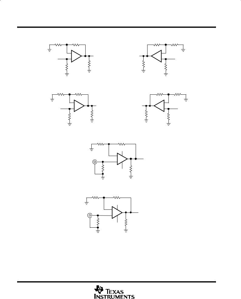
PARAMETER MEASUREMENT INFORMATION
1 kΩ |
1 kΩ |
|
|
1 kΩ |
1 kΩ |
|
Driver 1 |
± |
VO |
VO |
± |
Driver 2 |
|
+ |
+ |
|||||
VI |
VI |
|||||
25 Ω |
25 Ω |
|||||
|
50 Ω |
50 |
Ω |
|||
|
|
|
Figure 1. Driver Input-to-Output Crosstalk Test Circuit
1 kΩ |
1 kΩ |
|
|
1 kΩ |
1 kΩ |
|
Receiver 1 |
± |
VO |
VO |
± |
Receiver 2 |
|
+ |
+ |
|||||
VI |
VI |
|||||
150 Ω |
150 Ω |
|||||
|
50 Ω |
50 |
Ω |
|||
|
|
|
Figure 2. Receiver Input-to-Output Crosstalk Test Circuit
RG |
RF |
|
|
|
15 V |
|
|
Driver |
± |
VO |
|
+ |
|||
VI |
|
||
50 Ω |
RL |
|
|
±15 V 25 Ω |
|
||
|
|
Figure 3. Driver Test Circuit, Gain = 1 + (RF/RG)
RG |
RF |
|
|
|
15 V |
|
|
Receiver |
± |
VO |
|
+ |
|||
VI |
|
||
50 Ω |
RL |
|
|
±15 V 150 Ω |
|
||
|
|
Figure 4. Receiver Test Circuit, Gain = 1 + (RF/RG)
8 |
POST OFFICE BOX 655303 •DALLAS, TEXAS 75265 |

THS6002
DUAL DIFFERENTIAL LINE DRIVERS AND RECEIVERS
SLOS202D± JANUARY 1998± REVISED JULY 1999
TYPICAL CHARACTERISTICS
Table of Graphs
|
|
|
|
FIGURE |
|
|
|
|
|
|
|
|
Supply current |
Driver and Receiver |
vs Supply voltage |
5 |
|
|
|
|
|
|
|
|
Input voltage noise |
Driver and Receiver |
vs Frequency |
6 |
|
|
|
|
|
|
|
|
Input current noise |
Driver and Receiver |
vs Frequency |
6 |
|
|
|
|
|
|
|
|
Closed-loop output impedance |
Driver and Receiver |
vs Frequency |
7 |
|
|
|
|
|
|
|
|
Peak-to-peak output voltage swing |
Driver |
vs Supply voltage |
8 |
|
|
|
|
|
||
|
Receiver |
vs Supply voltage |
31 |
||
|
|
||||
|
|
|
|
|
|
|
Peak-to-peak output voltage |
Driver |
vs Load resistance |
9 |
|
|
|
|
|
||
|
Receiver |
vs Load resistance |
32 |
||
|
|
||||
|
|
|
|
|
|
VIO |
Input offset voltage |
Driver |
vs Free-air temperature |
10 |
|
|
|
|
|||
Receiver |
vs Free-air temperature |
33 |
|||
|
|
||||
|
|
|
|
|
|
IIB |
Input bias current |
Driver |
vs Free-air temperature |
11 |
|
|
|
|
|||
Receiver |
vs Free-air temperature |
34 |
|||
|
|
||||
|
|
|
|
|
|
CMMR |
Common-mode rejection ratio |
Driver |
vs Free-air temperature |
12 |
|
|
|
|
|||
Receiver |
vs Free-air temperature |
35 |
|||
|
|
||||
|
|
|
|
|
|
|
Input-to-output crosstalk |
Driver |
vs Frequency |
13 |
|
|
|
|
|
||
|
Receiver |
vs Frequency |
36 |
||
|
|
||||
|
|
|
|
|
|
|
Driver-to-receiver crosstalk |
|
vs Frequency |
14 |
|
|
|
|
|
|
|
|
Receiver-to-driver crosstalk |
|
vs Frequency |
37 |
|
|
|
|
|
|
|
PSSR |
Power supply rejection ratio |
Driver |
vs Free-air temperature |
15 |
|
|
|
|
|||
Receiver |
vs Free-air temperature |
38 |
|||
|
|
||||
|
|
|
|
|
|
ICC |
Supply current |
Driver |
vs Free-air temperature |
16 |
|
|
|
|
|||
Receiver |
vs Free-air temperature |
39 |
|||
|
|
||||
|
|
|
|
|
|
|
Normalized frequency response |
Driver |
vs Frequency |
17, 18 |
|
|
|
|
|
||
|
Receiver |
vs Frequency |
40, 41 |
||
|
|
||||
|
|
|
|
|
|
|
Normalized output response |
Driver |
vs Frequency |
19 ± 22 |
|
|
|
|
|
|
|
|
Single-ended output distortion |
Driver |
vs Output voltage |
23 |
|
|
|
|
|
|
|
|
Output distortion |
Receiver |
vs Output voltage |
42 |
|
|
|
|
|
|
|
|
Small and large signal frequency response |
Receiver |
|
43, 44 |
|
|
|
|
|
|
|
|
|
Driver |
DC input offset voltage |
24, 25 |
|
|
|
|
|
||
|
Differential gain |
Number of 150-Ω loads |
26, 27 |
||
|
|
||||
|
|
|
|
||
|
Receiver |
DC input offset voltage |
45, 46 |
||
|
|
||||
|
|
|
|
||
|
|
Number of 150-Ω loads |
47, 48 |
||
|
|
|
|||
|
|
|
|
|
|
|
|
Driver |
DC input offset voltage |
24, 25 |
|
|
|
|
|
||
|
Differential phase |
Number of 150-Ω loads |
26, 27 |
||
|
|
||||
|
|
|
|
||
|
Receiver |
DC input offset voltage |
45, 46 |
||
|
|
||||
|
|
|
|
||
|
|
Number of 150-Ω loads |
47, 48 |
||
|
|
|
|||
|
Output step response |
Driver |
|
28 ± 30 |
|
|
|
|
|
||
|
Receiver |
|
49 ± 51 |
||
|
|
|
POST OFFICE BOX 655303 •DALLAS, TEXAS 75265 |
9 |

THS6002
DUAL DIFFERENTIAL LINE DRIVERS AND RECEIVERS
SLOS202D± JANUARY 1998± REVISED JULY 1999
TYPICAL CHARACTERISTICS
I CC ± Supply Current ± mA
DRIVER AND RECEIVER |
DRIVER AND RECEIVER |
SUPPLY CURRENT |
INPUT VOLTAGE AND CURRENT NOISE |
|
|
|
|
|
vs |
|
|
|
|
|
|
|
vs |
|
|
|
|
|
|
SUPPLY VOLTAGE |
|
|
|
|
|
FREQUENCY |
|
|
|
||||
12 |
|
|
|
|
|
|
|
|
|
|
100 |
|
|
VCC = ±15 V |
100 |
|
11 |
|
|
|
|
|
|
|
|
|
|
|
|
|
|
|
|
|
|
|
|
|
|
|
|
|
|
|
|
|
TA = 25°C |
|
|
|
10 |
|
|
|
Driver |
|
|
|
|
|
|
|
|
|
|
|
|
|
|
|
|
|
|
|
|
|
|
|
|
|
|
|
||
|
|
|
|
|
|
|
|
|
|
|
|
|
|
|
|
|
9 |
|
|
|
|
|
|
|
|
|
Hz |
|
|
|
In± Noise |
|
Hz |
8 |
|
|
|
|
|
|
|
|
|
nV/ |
|
|
|
|
pA/ |
|
|
|
|
|
|
|
|
|
|
|
|
|
|
|
|
|
|
7 |
|
|
|
|
|
|
|
|
|
± |
|
|
|
|
|
± |
|
|
|
|
|
|
|
|
|
Noise |
|
|
|
|
|
Noise |
|
6 |
|
|
|
|
|
|
|
|
|
10 |
|
|
In+ Noise |
10 |
||
5 |
|
|
|
Receiver |
|
|
|
|
Voltage± |
|
|
|
|
|
Current± |
|
|
|
|
|
|
|
|
|
|
|
|
|
|
|
|||
4 |
|
|
|
|
|
|
|
|
|
|
|
|
|
|
|
|
3 |
|
|
|
|
|
|
|
|
|
n |
|
|
|
|
n |
|
|
TA = 25°C |
|
|
|
|
|
|
|
V |
|
|
|
|
|
I |
|
2 |
|
|
|
|
|
|
|
|
|
|
|
V Noise |
|
|
||
|
RF = 1 kΩ |
|
|
|
|
|
|
|
|
|
|
|
n |
|
|
|
1 |
|
|
|
|
|
|
|
|
|
|
|
|
|
|
||
Gain = +1 |
|
|
|
|
|
|
|
|
|
|
|
|
|
|
||
|
|
|
|
|
|
|
|
|
|
|
|
|
|
|
||
0 |
6 |
7 |
8 |
9 |
10 |
11 |
12 |
13 |
14 |
15 |
1 |
|
|
|
1 |
|
5 |
10 |
100 |
1k |
10k |
100k |
|
||||||||||
|
|
± VCC ± Supply Voltage ± V |
|
|
|
|
||||||||||
|
|
|
|
|
|
|
f ± Frequency ± Hz |
|
|
|
||||||
Figure 5 |
Figure 6 |
DRIVER AND RECEIVER
CLOSED-LOOP OUTPUT IMPEDANCE
|
|
|
|
vs |
|
|
|
|
|
|
|
|
FREQUENCY |
|
|
|
|
|
200 |
VCC = ±15 V |
|
|
|
|
|
|
|
100 |
|
|
|
|
|
||
|
|
RF = 1 kΩ |
|
|
|
|
|
|
± Ω |
|
Gain = 2 |
|
|
|
|
|
|
10 |
TA = 25°C |
|
|
|
|
|
||
Impedance |
VI(PP) = 1 V |
|
|
|
|
|
||
|
|
|
|
|
|
|||
|
|
Receiver |
|
|
|
|
||
1 |
|
|
|
|
Driver |
|
|
|
Output |
0.1 |
|
|
|
|
|
|
|
-Loop |
|
|
|
|
|
VO |
|
|
|
|
|
|
1 kΩ |
|
|||
|
|
|
1 kΩ |
|
|
|||
|
|
|
± |
1 kΩ |
|
|||
|
|
|
|
|
||||
Closed |
|
|
|
|
+ |
|
VI |
|
0.01 |
|
|
|
THS6002 |
|
|
||
|
|
|
|
|
|
|||
|
|
50 Ω |
|
1000 |
|
|||
|
|
|
|
|
||||
|
|
|
|
|
|
Zo = (VVOI |
± 1 ) |
|
|
0.001 |
|
|
|
|
|
|
500M |
|
100k |
1M |
10M |
|
100M |
|||
|
|
|
|
f ± Frequency ± Hz |
|
|
||
Figure 7
10 |
POST OFFICE BOX 655303 •DALLAS, TEXAS 75265 |
VO(PP) ± Peak-to-Peak Output Voltage Swing ± V
THS6002
DUAL DIFFERENTIAL LINE DRIVERS AND RECEIVERS
SLOS202D± JANUARY 1998± REVISED JULY 1999
TYPICAL CHARACTERISTICS
DRIVER |
DRIVER |
PEAK-TO-PEAK OUTPUT VOLTAGE SWING |
PEAK-TO-PEAK OUTPUT VOLTAGE |
vs |
vs |
SUPPLY VOLTAGE |
LOAD RESISTANCE |
15 |
|
|
|
|
|
|
|
|
|
|
15 |
|
|
|
|
|
|
|
|
|
|
|
|
V |
|
VCC = ±15 V |
|
10 |
|
|
|
|
|
|
|
|
|
± |
10 |
|
|
|
|
|
|
|
|
|
|
|
Voltage |
|
|
||
|
|
|
|
|
|
|
|
|
|
5 |
VCC = ±5 V |
|
|
5 |
|
|
|
|
|
|
|
|
|
Output |
|
||
|
|
|
|
|
|
|
|
|
|
|
TA = 25°C |
|
|
|
|
|
|
|
|
|
|
|
|
Peak |
|
Gain = 1 |
|
0 |
|
|
|
|
|
|
|
|
|
|
0 |
RF = 1 kΩ |
|
|
|
|
|
|
|
|
|
|
|
-to- |
|
|
|
±5 |
|
|
|
|
|
|
|
|
|
Peak± |
±5 |
VCC = ±5 V |
|
|
|
|
|
|
|
|
|
|
|
|
|||
±10 |
TA = 25°C |
|
|
|
|
|
|
|
O(PP) |
±10 |
|
|
|
RF = 1 kΩ |
|
|
|
|
|
|
|
|
|
||||
|
RL = 25 Ω |
|
|
|
|
|
|
|
V |
|
VCC = ±15 V |
|
|
|
Gain = 1 |
|
|
|
|
|
|
|
|
±15 |
|
|
|
±15 |
6 |
7 |
8 |
9 |
10 |
11 |
12 |
13 |
14 |
15 |
100 |
1000 |
|
5 |
10 |
||||||||||||
|
|
VCC ± Supply Voltage ± V |
|
|
|
|
RL ± Load Resistance ± Ω |
|
|||||
|
|
|
|
Figure 8 |
|
|
|
|
|
|
|
|
Figure 9 |
|
|
|
|
|
|
|
|
DRIVER |
|
|
|
|
|
|
|
DRIVER |
|
|
|
||
|
|
|
INPUT OFFSET VOLTAGE |
|
|
|
|
|
INPUT BIAS CURRENT |
|
|
||||||
|
|
|
|
vs |
|
|
|
|
|
|
|
|
|
vs |
|
|
|
|
|
|
FREE-AIR TEMPERATURE |
|
|
|
|
|
FREE-AIR TEMPERATURE |
|
|
||||||
|
2 |
|
|
|
|
|
|
|
|
5 |
G = 1 |
|
|
VCC = ±15 V |
|
|
|
|
|
G = 1 |
|
|
|
|
|
|
|
|
|
|
|
|
|||
|
|
|
|
|
|
|
|
|
|
RF = 1 kΩ |
|
IIB+ |
|
|
|
||
|
1 |
RF = 1 kΩ |
|
|
|
|
|
|
|
See Figure 2 |
|
|
|
|
|
||
±mV |
|
|
|
|
|
|
|
|
A |
4 |
|
|
|
|
|
|
|
0 |
|
|
|
|
V = ±5 V |
|
|
|
|
|
|
VCC = ±5 V |
|
||||
VoltageOffset |
|
|
|
|
CC |
|
|
CurrentBias± |
|
|
|
|
|
IIB+ |
|
|
|
±2 |
|
|
|
|
|
|
|
|
|
|
|
|
|
|
|||
|
|
|
|
|
|
|
|
|
|
|
|
|
|
|
|
|
|
|
±1 |
|
|
|
|
|
|
|
|
3 |
|
|
|
|
|
|
|
|
|
|
|
|
|
|
|
|
|
|
|
|
|
|
|
|
|
Input± |
±3 |
|
|
VCC = ±15 V |
|
|
|
Input± |
2 |
|
|
|
|
|
|
|
|
|
|
|
|
|
|
|
|
|
|
|
|
|
|||||
|
|
|
|
|
|
|
|
|
|
|
|
|
|
|
|
||
IO |
|
|
|
|
|
|
|
|
IB |
1 |
|
VCC = ±5 V |
|
VCC = ±15 V |
|
||
V |
|
|
|
|
|
|
|
|
I |
|
IIB± |
|
|
IIB± |
|
|
|
|
±4 |
|
|
|
|
|
|
|
|
|
|
|
|
|
|
||
|
|
|
|
|
|
|
|
|
|
|
|
|
|
|
|
|
|
|
±5 |
|
|
|
|
|
|
|
|
0 |
|
|
|
|
|
|
|
|
±40 |
±20 |
0 |
20 |
40 |
60 |
80 |
100 |
|
±40 |
±20 |
0 |
20 |
40 |
60 |
80 |
100 |
|
|
|
TA ± Free-Air Temperature ± °C |
|
|
|
|
|
TA ± Free-Air Temperature ± °C |
|
|
||||||
Figure 10 |
Figure 11 |
|
|
|
|
POST OFFICE BOX 655303 •DALLAS, TEXAS 75265 |
11 |

THS6002
DUAL DIFFERENTIAL LINE DRIVERS AND RECEIVERS
SLOS202D± JANUARY 1998± REVISED JULY 1999
TYPICAL CHARACTERISTICS
DRIVER |
DRIVER |
COMMON-MODE REJECTION RATIO |
INPUT-TO-OUTPUT CROSSTALK |
vs |
vs |
FREE-AIR TEMPERATURE |
FREQUENCY |
± dB |
80 |
|
|
|
|
|
|
|
|
|
|
|
|
|
|
±CrosstalkOutput-to-InputdB |
|
RejectionMode-Common±CMRRRatio |
75 |
|
|
1 kΩ |
|
|
|
|
|
|
|
|
|
|
|
|
|
|
|
|
|
VCC = ±15 V |
|
|
||
|
70 |
|
|
|
|
|
|
|
|
|
|
|
VCC = ±5 V |
|
|
||
|
|
|
|
1 kΩ |
|
|
|
|
|
65 |
|
1 kΩ |
± |
|
|
|
|
|
|
VI |
|
V |
O |
|
|
|
|
|
|
+ |
|
|
|
||
|
|
|
1 kΩ |
|
|
|
|
|
|
60 |
|
|
|
|
|
|
|
|
±40 |
±20 |
0 |
20 |
|
40 |
60 |
80 |
|
|
|
TA ± Free-Air Temperature ± °C |
|
||||
0 |
|
|
|
|
|
|
|
|
|
|
|
|
|
|
|
|
|
|
|
|
|
|
|
|
|
|
|
|
|
|
|
|
|
|
|
|
|
|
|
|
|
|
|
|
|
|
|
|
|
VCC = ±15 |
|
|
V |
|
|
|
|
|
|
|
|
|
|
|
|||||||
±10 |
|
RF = 1 kΩ |
|
|
|
|
|
|
|
|
|
|
|
|
|||||||||
|
|
|
|
|
|
|
|
|
|
|
|
|
|||||||||||
|
|
RL = 25 Ω |
|
|
|
|
|
|
|
|
|
|
|
||||||||||
±20 |
|
Gain = 2 |
|
|
|
|
|
|
|
|
|
|
|
|
|||||||||
|
VI = 200 mV |
|
|
|
|
|
|
|
|
|
|
|
|||||||||||
|
|
|
|
|
|
|
|
|
|
|
|
|
|||||||||||
±30 |
|
See Figure 1 |
|
|
|
|
|
|
|
|
|
|
|
||||||||||
|
|
|
|
|
|
|
|
|
|
|
|
|
|
|
|
|
|
|
|
|
|
|
|
±40 |
|
|
|
|
|
|
|
|
|
|
|
|
|
|
|
|
|
|
|
|
|
|
|
|
|
|
|
|
|
|
|
|
|
|
|
Driver 1 = Output |
|||||||||||
|
|
|
|
|
|
|
|
|
|
|
|
||||||||||||
|
|
|
|
|
|
|
|
|
|
|
|
|
Driver 2 = Input |
||||||||||
±50 |
|
|
|
|
±60 |
|
|
|
|
±70 |
|
|
|
|
±80 |
|
Driver 1 |
= Input |
|
|
Driver 2 |
= Output |
|
|
|
|
|
||
±90 |
|
|
|
|
100k |
1M |
10M |
100M |
500M |
|
|
f ± Frequency ± Hz |
|
|
Figure 12 |
Figure 13 |
DRIVER-TO-RECEIVER CROSSTALK |
DRIVER |
POWER SUPPLY REJECTION RATIO |
|
|
|
|
|
vs |
|
|
|
|
|
|
vs |
|
|
|
|
|
|
|
|
|
FREQUENCY |
|
|
|
|
|
FREE-AIR TEMPERATURE |
|
|
|||
|
0 |
VCC = ±15 V |
|
|
|
|
95 |
|
|
|
|
|
|
|
||
|
|
|
|
|
|
|
|
|
|
|
|
|
||||
|
|
|
|
|
dB |
|
G = 1 |
|
|
|
|
|
|
|||
|
±10 |
R |
F |
= 1 kΩ |
|
|
|
|
RF = 1 kΩ |
|
|
|
|
|
||
|
|
|
|
|
|
± |
|
|
|
|
|
|
||||
CrosstalkReceiver-to-Driver± dB |
|
Gain = 2 |
|
|
|
RejectionSupplyPower±PSRRRatio |
90 |
|
|
|
|
|
|
|
||
±20 |
VI = 200 mV |
|
|
|
|
|
|
|
|
|
|
|||||
|
|
|
|
|
|
|
|
|
|
|
||||||
|
See Figures 1 and 2 |
|
|
|
|
|
|
|
|
|
|
|||||
±30 |
|
|
|
|
|
|
85 |
|
|
|
|
|
|
|
||
|
|
|
|
|
|
|
|
|
|
|
|
|
|
|
||
|
|
Receiver 2 = Output |
|
|
|
|
|
|
|
|
|
|
||||
|
|
|
|
|
|
|
VCC = 15 V |
|
|
|
|
|||||
|
±40 Driver 2 = Input |
|
|
|
|
|
|
|
|
|
|
|||||
|
|
|
|
|
|
|
|
|
|
|
|
|
||||
|
|
|
|
|
Receiver 1 = Output |
|
|
80 |
VCC = 5 V |
|
|
|
|
|||
|
±50 |
|
|
|
Driver 1 = Input |
|
|
|
|
|
|
|
||||
|
|
|
|
|
|
|
|
|
|
|
|
|
|
|
|
|
|
±60 |
|
|
|
|
|
|
|
75 |
|
|
|
|
VCC = ±5 V |
|
|
|
|
|
|
|
|
|
|
|
|
|
|
|
|
|||
|
±70 |
|
|
|
Receiver 1 = Output |
|
|
|
|
|
|
|
|
|
|
|
|
|
|
|
Driver 2 = Input |
|
|
|
|
|
VCC = ±15 V |
|
|
|
|
||
|
|
|
|
|
|
|
|
|
|
|
|
|
|
|||
|
|
|
|
Receiver 2 = Output |
|
|
|
70 |
|
|
|
|
|
|||
|
±80 |
|
|
|
|
|
|
|
|
|
|
|
|
|||
|
|
|
Driver 1 = Input |
|
|
|
|
|
|
|
|
|
|
|
||
|
|
|
|
|
|
|
|
|
|
|
|
|
|
|
||
|
±90 |
|
|
|
|
|
|
|
65 |
|
|
|
|
|
|
|
|
100k |
|
1M |
10M |
100M |
500M |
|
|
|
|
|
|
|
|
||
|
|
|
±40 |
±20 |
0 |
20 |
40 |
60 |
80 |
100 |
||||||
|
|
|
|
|
f ± Frequency ± Hz |
|
|
|
|
|
TA ± Free-Air Temperature ± °C |
|
|
|||
|
|
|
|
|
|
|
|
|
|
|
|
|
||||
|
|
|
|
|
Figure 14 |
|
|
|
|
|
|
Figure 15 |
|
|
|
|
12 |
POST OFFICE BOX 655303 •DALLAS, TEXAS 75265 |
 Loading...