


THS5661A 12-BIT, 125 MSPS, CommsDAC
DIGITAL-TO-ANALOG CONVERTER
SLAS247 ± NOVEMBER 1999
DMember of the Pin-Compatible CommsDAC Product Family
D125 MSPS Update Rate
D12-Bit Resolution
DSpurious Free Dynamic Range (SFDR) to Nyquist at 40 MHz Output: 60 dBc
D1 ns Setup/Hold Time
DDifferential Scalable Current Outputs: 2 mA to 20 mA
DOn-Chip 1.2 V Reference
D3 V and 5 V CMOS-Compatible Digital Interface
DStraight Binary or Twos Complement Input
DPower Dissipation: 175 mW at 5 V, Sleep Mode: 25 mW at 5 V
SOIC (DW) OR TSSOP (PW) PACKAGE
(TOP VIEW)
D11 |
|
|
1 |
28 |
|
|
CLK |
|
|
|
|
||||
D10 |
|
|
2 |
27 |
|
|
DVDD |
|
|
|
|
||||
|
|
|
|
||||
D9 |
|
|
3 |
26 |
|
|
DGND |
D8 |
|
4 |
25 |
|
|
MODE |
|
|
|
|
|
||||
D7 |
|
5 |
24 |
|
|
AVDD |
|
|
|
|
|
||||
|
|
|
|
||||
D6 |
|
|
6 |
23 |
|
|
COMP2 |
D5 |
|
|
7 |
22 |
|
|
IOUT1 |
|
|
|
|
||||
D4 |
|
8 |
21 |
|
|
IOUT2 |
|
|
|
|
|
||||
D3 |
|
9 |
20 |
|
|
AGND |
|
|
|
|
|
||||
D2 |
|
10 |
19 |
|
|
COMP1 |
|
|
|
|
|
||||
D1 |
|
11 |
18 |
|
|
BIASJ |
|
|
|
|
|
||||
D0 |
|
|
12 |
17 |
|
|
EXTIO |
|
|
|
|
||||
NC |
13 |
16 |
|
|
EXTLO |
||
NC |
14 |
15 |
|
|
SLEEP |
||
|
|
|
|
|
|
|
|
D Package: 28-Pin SOIC and TSSOP |
NC ± No internal connection |
|
description
The THS5661A is a 12-bit resolution digital-to-analog converter (DAC) specifically optimized for digital data transmission in wired and wireless communication systems. The 12-bit DAC is a member of the CommsDAC series of high-speed, low-power CMOS digital-to-analog converters. The CommsDAC family consists of pin compatible 14-, 12-, 10-, and 8-bit DACs. All devices offer identical interface options, small outline package, and pinout. The THS5661A offers superior ac and dc performance while supporting update rates up to 125 MSPS.
The THS5661A operates from an analog supply of 4.5 V to 5.5 V. Its inherent low power dissipation of 175 mW ensures that the device is well-suited for portable and low-power applications. Lowering the full-scale current output reduces the power dissipation without significantly degrading performance. The device features a SLEEP mode, which reduces the standby power to approximately 25 mW, thereby optimizing the power consumption for system needs.
The THS5661A is manufactured in Texas Instruments advanced high-speed mixed-signal CMOS process. A current-source-array architecture combined with simultaneous switching shows excellent dynamic performance. On-chip edge-triggered input latches and a 1.2 V temperature-compensated bandgap reference provide a complete monolithic DAC solution. The digital supply range of 3 V to 5.5 V supports 3 V and 5 V CMOS logic families. Minimum data input setup and hold times allow for easy interfacing with external logic. The THS5661A supports both a straight binary and twos complement input word format, enabling flexible interfacing with digital signal processors.
The THS5661A provides a nominal full-scale differential output current of 20 mA and >300 kΩ output impedance, supporting both single-ended and differential applications. The output current can be directly fed to the load (e.g., external resistor load or transformer), with no additional external output buffer required. An accurate on-chip reference and control amplifier allows the user to adjust this output current from 20 mA down to 2 mA, with no significant degradation of performance. This reduces power consumption and provides 20 dB gain range control capabilities. Alternatively, an external reference voltage and control amplifier may be applied in applications using a multiplying DAC. The output voltage compliance range is 1.25 V.
Please be aware that an important notice concerning availability, standard warranty, and use in critical applications of Texas Instruments semiconductor products and disclaimers thereto appears at the end of this data sheet.
CommsDAC is a trademark of Texas Instruments Incorporated.
PRODUCTION DATA information is current as of publication date. Products conform to specifications per the terms of Texas Instruments standard warranty. Production processing does not necessarily include testing of all parameters.
Copyright 1999, Texas Instruments Incorporated
POST OFFICE BOX 655303 •DALLAS, TEXAS 75265 |
1 |
THS5661A
12-BIT, 125 MSPS, CommsDAC
DIGITAL-TO-ANALOG CONVERTER
SLAS247 ± NOVEMBER 1999
description (continued)
The THS5661A is available in both a 28-pin SOIC and TSSOP package. The device is characterized for operation over the industrial temperature range of ±40°C to 85°C.
AVAILABLE OPTIONS
|
PACKAGE |
|
TA |
|
|
28-TSSOP |
28-SOIC |
|
|
(PW) |
(DW) |
|
|
|
± 40°C to 85°C |
THS5661AIPW |
THS5661AIDW |
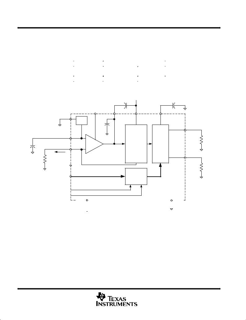
functional block diagram
|
|
|
C1 |
AVDD |
|
|
|
|
|
|
|
|
SLEEP |
COMP1 |
0.1 µF |
COMP2 |
0.1 µF |
EXTLO |
1.2 V |
|
|
|
|
|
|
|
|
|
|
|
REF |
|
|
|
|
|
|
1 nF |
|
|
IOUT1 |
|
|
|
|
|
|
|
|
EXTIO |
± |
|
|
Output |
50 Ω |
RLOAD |
CEXT |
|
Current |
||||
|
|
Source |
Current |
|
|
|
BIASJ |
+ |
Control |
Array |
Switches |
|
|
0.1 µF |
|
AMP |
|
|
|
|
I BIAS |
|
|
|
IOUT2 |
|
|
|
|
|
|
|
||
2 kΩ RBIAS |
|
|
|
|
|
|
DVDD |
|
|
|
|
50 Ω |
RLOAD |
Logic
D[11:0]
Control
MODE 
CLK 
|
|
|
|
|
|
|
|
|
|
|
|
|
|
|
|
|
|
|
|
|
|
|
|
|
|
|
|
|
|
|
|
|
|
|
|
|
|
|
|
|
|
|
|
|
|
|
|
|
|
|
|
|
|
|
|
|
|
|
|
|
|
|
|
|
|
|
|
|
|
|
|
|
|
|
DGND |
|
|
|
|
|
|
|
|
|
|
|
|
|
|
|
|
|
|
|
|
|
|
|
|
|
|
|
|
|
|
|
|
|
|
|
|
|
|
|
|
|
|
|
|
|
|
|
|
|
|
|
|
|
|
|
|
|
|
|
|
AGND |
|||||||||||||
|
|
|
|
|
|
|
|
|
|
|
|
|
|
|
|
|
|
|
|
|
|
|
|
|
|
|
|
|
|
|
|
|
|
|
|
|
|
|
|
|
|
|
|
|
|
|
|
|
|
|
|
|
|
|
|
|
|
|
|
|
|
|
|
|
|
|
|
|
|
|
|
|
|
|
|
|
|
|
|
|
|
|
|
|
|
|
|
|
|
|
|
|
|
|
|
|
|
|
|
|
|
|
|
|
|
|
|
|
|
|
|
|
|
|
|
|
|
|
|
|
|
|
|
|
|
|
|
|
|
|
|
|
|
|
|
|
|
|
|
|
|
|
|
|
|
|
|
|
|
2 |
POST OFFICE BOX 655303 •DALLAS, TEXAS 75265 |

|
|
|
THS5661A |
|
|
|
|
12-BIT, 125 MSPS, CommsDAC |
|
|
|
|
DIGITAL-TO-ANALOG CONVERTER |
|
|
|
|
SLAS247 ± NOVEMBER 1999 |
|
|
|
|
|
|
|
|
|
Terminal Functions |
|
|
|
|
|
|
TERMINAL |
I/O |
DESCRIPTION |
|
|
NAME |
NO. |
|
||
|
|
|
||
|
|
|
|
|
AGND |
20 |
I |
Analog ground return for the internal analog circuitry |
|
|
|
|
|
|
AVDD |
24 |
I |
Positive analog supply voltage (4.5 V to 5.5 V) |
|
BIASJ |
18 |
O |
Full-scale output current bias |
|
|
|
|
|
|
CLK |
28 |
I |
External clock input. Input data latched on rising edge of the clock. |
|
|
|
|
|
|
COMP1 |
19 |
I |
Compensation and decoupling node, requires a 0.1 F capacitor to AVDD. |
|
COMP2 |
23 |
I |
Internal bias node, requires a 0.1 F decoupling capacitor to AGND. |
|
|
|
|
|
|
D[11:0] |
[1:12] |
I |
Data bits 0 through 11. |
|
|
|
|
D11 is most significant data bit (MSB), D0 is least significant data bit (LSB). |
|
|
|
|
|
|
DGND |
26 |
I |
Digital ground return for the internal digital logic circuitry |
|
|
|
|
|
|
DVDD |
27 |
I |
Positive digital supply voltage (3 V to 5.5 V) |
|
EXTIO |
17 |
I/O |
Used as external reference input when internal reference is disabled (i.e., EXTLO = AVDD). Used as internal |
|
|
|
|
reference output when EXTLO = AGND, requires a 0.1 F decoupling capacitor to AGND when used as reference |
|
|
|
|
output. |
|
|
|
|
|
|
EXTLO |
16 |
O |
Internal reference ground. Connect to AVDD to disable the internal reference source. |
|
IOUT1 |
22 |
O |
DAC current output. Full scale when all input bits are set 1 |
|
|
|
|
|
|
IOUT2 |
21 |
O |
Complementary DAC current output. Full scale when all input bits are 0 |
|
|
|
|
|
|
MODE |
25 |
I |
Mode select. Internal pulldown. Mode 0 is selected if this pin is left floating or connected to DGND. See |
|
|
|
|
timing diagram. |
|
|
|
|
|
|
NC |
[13:14] |
N |
No connection |
|
|
|
|
|
|
SLEEP |
15 |
I |
Asynchronous hardware power down input. Active high. Internal pulldown. Requires 5 s to power down but 3 ms |
|
|
|
|
to power up. |
|
|
|
|
|
|
absolute maximum ratings over operating free-air temperature (unless otherwise noted)²
Supply voltage range, AVDD (see Note 1) . . . . . . . . . . . . . . . . . . . . . . . . . . . . . . . . . . . . . |
. . . . . . . ±0.3 V to 6.5 V |
DVDD (see Note 2) . . . . . . . . . . . . . . . . . . . . . . . . . . . . . . . . . . . . |
. . . . . . . ±0.3 V to 6.5 V |
Voltage between AGND and DGND . . . . . . . . . . . . . . . . . . . . . . . . . . . . . . . . . . . . . . . . . . |
. . . . . . . ±0.3 V to 0.5 V |
Supply voltage range, AVDD to DVDD . . . . . . . . . . . . . . . . . . . . . . . . . . . . . . . . . . . . . . . . |
. . . . . . . ±6.5 V to 6.5 V |
CLK, SLEEP, MODE (see Note 2) . . . . . . . . . . . . . . . . . . . . . . |
±0.3 V to DVDD + 0.3 V |
Digital input D11±D0 (see Note 2) . . . . . . . . . . . . . . . . . . . . . |
±0.3 V to DVDD + 0.3 V |
IOUT1, IOUT2 (see Note 1) . . . . . . . . . . . . . . . . . . . . . . . . . . . . . |
. ±1 V to AVDD + 0.3 V |
COMP1, COMP2 (see Note 1) . . . . . . . . . . . . . . . . . . . . . . . . . |
±0.3 V to AVDD + 0.3 V |
EXTIO, BIASJ (see Note 1) . . . . . . . . . . . . . . . . . . . . . . . . . . . . |
±0.3 V to AVDD + 0.3 V |
EXTLO (see Note 1) . . . . . . . . . . . . . . . . . . . . . . . . . . . . . . . . . . . |
. . . . . . . ±0.3 V to 0.3 V |
Peak input current (any input) . . . . . . . . . . . . . . . . . . . . . . . . . . . . . . . . . . . . . . . . . . . . . . . |
. . . . . . . . . . . . . . 20 mA |
Peak total input current (all inputs) . . . . . . . . . . . . . . . . . . . . . . . . . . . . . . . . . . . . . . . . . . . |
. . . . . . . . . . . . . ±30 mA |
Operating free-air temperature range, TA: THS5661AI . . . . . . . . . . . . . . . . . . . . . . . . . . |
. . . . . . . ±40°C to 85°C |
Storage temperature range . . . . . . . . . . . . . . . . . . . . . . . . . . . . . . . . . . . . . . . . . . . . . . . . . . |
. . . . . . ±65°C to 150°C |
Lead temperature 1,6 mm (1/16 inch) from the case for 10 seconds . . . . . . . . . . . . . . |
. . . . . . . . . . . . . . 260°C |
² Stresses beyond those listed under ªabsolute maximum ratingsº may cause permanent damage to the device. These are stress ratings only, and functional operation of the device at these or any other conditions beyond those indicated under ªrecommended operating conditionsº is not implied. Exposure to absolute-maximum-rated conditions for extended periods may affect device reliability.
NOTES: 1. Measured with respect to AGND. 2. Measured with respect to DGND.
POST OFFICE BOX 655303 •DALLAS, TEXAS 75265 |
3 |

THS5661A
12-BIT, 125 MSPS, CommsDAC
DIGITAL-TO-ANALOG CONVERTER
SLAS247 ± NOVEMBER 1999
electrical characteristics over recommended operating free-air temperature range, AVDD = 5 V, DVDD = 5 V, IOUTFS = 20 mA (unless otherwise noted)
dc specifications
|
|
|
PARAMETER |
|
|
|
|
TEST CONDITIONS |
MIN |
TYP |
MAX |
UNIT |
||||
|
|
|
|
|
|
|
|
|
|
|
|
|
|
|
|
|
Resolution |
|
|
|
|
|
|
|
|
|
|
|
12 |
|
|
Bits |
|
|
|
|
|
|
|
|
|
|
|
|
|
|
|
|
|
|
DC accuracy² |
|
|
|
|
|
|
|
|
|
|
|
|
|
|
||
INL |
Integral nonlinearity |
|
|
TA = ±40°C to 85°C |
|
±4 |
±0.75 |
4 |
LSB |
|||||||
|
|
|
|
|
|
|
|
|
|
|
|
|
|
|||
DNL |
Differential nonlinearity |
|
|
|
±2 |
±0.5 |
2 |
LSB |
||||||||
|
|
|
|
|
|
|||||||||||
|
|
|
|
|
|
|
|
|
|
|
|
|
|
|
|
|
Monotonicity |
|
|
|
|
|
|
|
At 11-bit level |
|
|
|
Monotonic |
|
|
||
|
|
|
|
|
|
|
|
|
|
|
|
|
|
|
|
|
Analog output |
|
|
|
|
|
|
|
|
|
|
|
|
|
|
||
|
|
|
|
|
|
|
|
|
|
|
|
|
||||
|
Offset error |
|
|
|
|
|
|
|
|
0.02 |
|
%FSR |
||||
|
|
|
|
|
|
|
|
|
|
|
|
|
|
|||
|
Gain error |
|
|
|
|
Without internal reference |
|
2.3 |
|
%FSR |
||||||
|
|
|
|
|
|
|
|
|
|
|
|
|||||
|
|
|
|
|
With internal reference |
|
|
1.3 |
|
|||||||
|
|
|
|
|
|
|
|
|
|
|
|
|
||||
|
|
|
|
|
|
|
|
|
|
|
|
|||||
|
Full scale output current³ |
|
|
|
|
|
|
2 |
|
20 |
mA |
|||||
|
Output compliance range |
|
|
AVDD = 5 V, |
IOUTFS = 20 mA |
±1 |
|
1.25 |
V |
|||||||
|
Output resistance |
|
|
|
|
|
|
|
300 |
|
kΩ |
|||||
|
Output capacitance |
|
|
|
|
|
|
|
5 |
|
pF |
|||||
|
|
|
|
|
|
|
|
|
|
|
|
|
|
|
||
Reference output |
|
|
|
|
|
|
|
|
|
|
|
|
|
|||
|
|
|
|
|
|
|
|
|
|
|
|
|||||
|
Reference voltage |
|
|
|
|
|
|
1.18 |
1.22 |
1.32 |
V |
|||||
|
|
|
|
|
|
|
|
|
|
|
||||||
|
Reference output current§ |
|
|
|
|
|
|
100 |
|
nA |
||||||
Reference input |
|
|
|
|
|
|
|
|
|
|
|
|
|
|
||
|
|
|
|
|
|
|
|
|
|
|
|
|||||
VEXTIO |
Input voltage range |
|
|
|
|
|
|
0.1 |
|
1.25 |
V |
|||||
|
Input resistance |
|
|
|
|
|
|
|
|
1 |
|
MΩ |
||||
|
|
|
|
|
|
|
|
|
|
|||||||
|
Small signal bandwidth¶ |
|
|
Without CCOMP1 |
|
|
1.3 |
|
MHz |
|||||||
|
Input capacitance |
|
|
|
|
|
|
|
100 |
|
pF |
|||||
|
|
|
|
|
|
|
|
|
|
|
|
|
||||
Temperature coefficients |
|
|
|
|
|
|
|
|
|
|
|
|||||
|
|
|
|
|
|
|
|
|
|
|
|
|
|
|||
|
Offset drift |
|
|
|
|
|
|
|
|
|
0 |
|
|
|||
|
|
|
|
|
|
|
|
|
|
|
|
|
|
|||
|
Gain drift |
|
|
|
|
Without internal reference |
|
±40 |
|
ppm of |
||||||
|
|
|
|
|
With internal reference |
|
|
±120 |
|
FSR/°C |
||||||
|
|
|
|
|
|
|
|
|
|
|
|
|||||
|
|
|
|
|
|
|
|
|
|
|
|
|
||||
|
|
|
|
|
|
|
|
|
|
|
|
|||||
|
Reference voltage drift |
|
|
|
|
|
|
|
±35 |
|
|
|||||
Power supply |
|
|
|
|
|
|
|
|
|
|
|
|
|
|
||
|
|
|
|
|
|
|
|
|
|
|
|
|||||
AVDD |
Analog supply voltage |
|
|
|
|
|
|
4.5 |
5 |
5.5 |
V |
|||||
DVDD |
Digital supply voltage |
|
|
|
|
|
|
3 |
|
5.5 |
V |
|||||
IAVDD |
Analog supply current |
|
|
|
|
|
|
|
25 |
30 |
mA |
|||||
|
|
|
|
|
|
|
|
|
|
|
|
|
|
|
|
|
Sleep mode supply current |
|
Sleep mode |
|
|
|
3 |
5 |
mA |
||||||||
|
|
|
|
|
||||||||||||
|
|
|
|
|
|
|
|
|
|
|
|
|||||
I |
Digital supply current# |
|
|
|
|
|
|
|
5 |
6 |
mA |
|||||
DVDD |
|
|
|
|
|
|
|
|
|
|
|
|
|
|
|
|
|
Power dissipation|| |
|
|
AVDD = 5 V, |
DVDD = 5 V, IOUTFS = 20 mA |
|
175 |
|
mW |
|||||||
AVDD |
Power supply rejection ratio |
|
|
|
|
|
|
±0.4 |
|
%FSR/V |
||||||
DVDD |
|
|
|
|
|
|
±0.025 |
|
||||||||
|
|
|
|
|
|
|
|
|
|
|
|
|
|
|
||
|
Operating range |
|
|
|
|
|
|
|
±40 |
|
85 |
°C |
||||
² Measured at IOUT1 in virtual ground configuration. |
|
|
|
|
|
|
|
|||||||||
³ Nominal full-scale current IOUTFS equals 32X the IBIAS current. |
|
|
|
|
|
|
||||||||||
§ Use an external buffer amplifier with high impedance input to drive any external load. |
|
|
|
|
||||||||||||
¶ Reference bandwidth is a function of external cap at COMP1 pin and signal level. |
|
|
|
|
||||||||||||
# Measured at f |
CLK |
= 50 MSPS and f |
= 1 MHz. |
|
|
|
|
|
|
|
|
|
||||
|
|
|
|
|
OUT |
|
|
|
|
|
|
|
|
|
||
|| Measured for 50 |
Ω R |
LOAD |
at IOUT1 and IOUT2, f |
CLK |
= 50 MSPS and f |
= 20 MHz. |
|
|
|
|
||||||
|
|
|
|
|
|
|
|
OUT |
|
|
|
|
|
|||
Specifications subject to change
4 |
POST OFFICE BOX 655303 •DALLAS, TEXAS 75265 |

THS5661A 12-BIT, 125 MSPS, CommsDAC
DIGITAL-TO-ANALOG CONVERTER
SLAS247 ± NOVEMBER 1999
electrical characteristics over recommended operating free-air temperature range, AVDD = 5 V, DVDD = 5 V, IOUTFS = 20 mA, differential transformer coupled output, 50 Ω doubly terminated load
(unless otherwise noted)
ac specifications
|
PARAMETER |
TEST CONDITIONS |
MIN |
TYP |
MAX |
UNIT |
|
|
|
|
|
|
|
Analog output |
|
|
|
|
|
|
|
|
|
|
|
|
|
fCLK |
Maximum output update rate |
DVDD = 4.5 V to 5.5 V |
100 |
125 |
|
MSPS |
DVDD = 3 V to 3.6 V |
70 |
100 |
|
|||
|
|
|
|
|||
t |
Output settling time to 0.1%² |
|
|
35 |
|
ns |
s(DAC) |
|
|
|
|
|
|
tpd |
Output propagation delay |
|
|
1 |
|
ns |
GE |
Glitch energy³ |
Worst case LSB transition (code 2047 ± code 2048) |
|
5 |
|
pV-s |
t |
Output rise time 10% to 90%² |
|
|
1 |
|
ns |
r(IOUT) |
|
|
|
|
|
|
t |
Output fall time 90% to 10%² |
|
|
1 |
|
ns |
f(IOUT) |
|
|
|
|
|
|
|
Output noise |
IOUTFS = 20 mA |
|
15 |
|
pA/√ HZ |
|
IOUTFS = 2 mA |
|
10 |
|
||
|
|
|
|
|
||
AC linearity |
|
|
|
|
|
|
|
|
|
|
|
|
|
|
|
fCLK = 25 MSPS, fOUT = 1 MHz, TA = 25°C |
|
±78 |
|
|
THD |
Total harmonic distortion |
fCLK = 50 MSPS, fOUT = 1 MHz, TA = ±40°C to 85°C |
|
±77 |
±66 |
dBc |
fCLK = 50 MSPS, fOUT = 2 MHz, TA = 25°C |
|
±75 |
|
|||
|
|
|
|
|
||
|
|
fCLK = 100 MSPS, fOUT = 2 MHz, TA = 25°C |
|
±75 |
|
|
|
|
fCLK = 25 MSPS, fOUT = 1 MHz, TA = 25°C |
|
82 |
|
|
|
|
fCLK = 50 MSPS, fOUT= 1 MHz, TA = ±40°C to 85°C |
68 |
|
|
|
|
|
fCLK = 50 MSPS, fOUT = 1 MHz, TA = 25°C |
|
79 |
|
dBc |
|
Spurious free dynamic range to |
fCLK = 50 MSPS, fOUT = 2.51 MHz, TA = 25°C |
|
75 |
|
|
|
|
|
|
|||
|
fCLK = 50 MSPS, fOUT = 5.02 MHz, TA = 25°C |
|
69 |
|
|
|
|
Nyquist |
|
|
|
||
SFDR |
fCLK = 50 MSPS, fOUT = 20.2 MHz, TA = 25°C |
|
61 |
|
|
|
|
|
|
|
|||
|
fCLK = 100 MSPS, fOUT = 5.04 MHz, TA = 25°C |
|
68 |
|
dBc |
|
|
|
|
|
|||
|
|
fCLK = 100 MSPS, fOUT = 20.2 MHz, TA = 25°C |
|
59 |
|
dBc |
|
|
fCLK = 100 MSPS, fOUT = 40.4 MHz, TA = 25°C |
|
60 |
|
dBc |
|
Spurious free dynamic range |
fCLK = 50 MSPS, fOUT = 1 MHz, TA= 25°C,1 MHz span |
|
89 |
|
|
|
fCLK = 50 MSPS, fOUT = 5.02 MHz, 2 MHz span |
|
88 |
|
dBc |
|
|
within a window |
|
|
|||
|
fCLK = 100 MSPS, fOUT= 5.04 MHz, 4 MHz span |
|
89 |
|
|
|
|
|
|
|
|
||
² Measured single ended into 50 Ω load at IOUT1. |
|
|
|
|
||
³ Single-ended output IOUT1, 50 Ω doubly terminated load. |
|
|
|
|
||
POST OFFICE BOX 655303 •DALLAS, TEXAS 75265 |
5 |

THS5661A
12-BIT, 125 MSPS, CommsDAC
DIGITAL-TO-ANALOG CONVERTER
SLAS247 ± NOVEMBER 1999
electrical characteristics over recommended operating free-air temperature range, AVDD = 5 V, DVDD = 5 V, IOUTFS = 20 mA (unless otherwise noted)
digital specifications
|
PARAMETER |
TEST CONDITIONS |
MIN |
TYP |
MAX |
UNIT |
|
|
|
|
|
|
|
Interface |
|
|
|
|
|
|
|
|
|
|
|
|
|
VIH |
High-level input voltage |
DVDD = 5 V |
3.5 |
5 |
|
V |
DVDD = 3.3 V |
2.1 |
3.3 |
|
|||
|
|
|
|
|||
VIL |
Low-level input voltage |
DVDD = 5 V |
|
0 |
1.3 |
V |
DVDD = 3.3 V |
|
0 |
0.9 |
|||
|
|
|
|
|||
IIH |
High-level input current |
DVDD = 3 V to 5.5 V |
±10 |
|
10 |
A |
IIL |
Low-level input current |
DVDD = 3 V to 5.5 V |
±10 |
|
10 |
A |
|
Input capacitance |
|
1 |
|
5 |
pF |
|
|
|
|
|
|
|
Timing |
|
|
|
|
|
|
|
|
|
|
|
|
|
tsu(D) |
Input setup time |
|
1 |
|
|
ns |
th(D) |
Input hold time |
|
1 |
|
|
ns |
tw(LPH) |
Input latch pulse high time |
|
4 |
|
|
ns |
td(D) |
Digital delay time |
|
|
|
1 |
clk |
Specifications subject to change
6 |
POST OFFICE BOX 655303 •DALLAS, TEXAS 75265 |
THS5661A 12-BIT, 125 MSPS, CommsDAC
DIGITAL-TO-ANALOG CONVERTER
SLAS247 ± NOVEMBER 1999
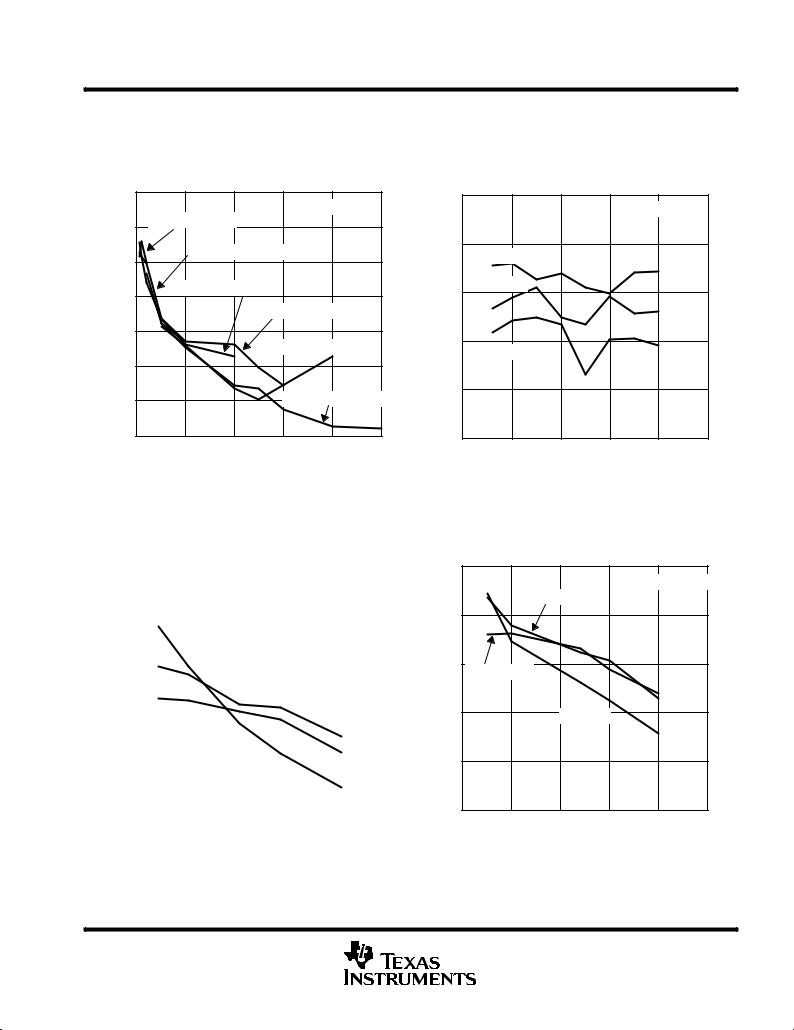
TYPICAL CHARACTERISTICS²
SPURIOUS FREE DYNAMIC RANGE vs
OUTPUT FREQUENCY AT 0 dBFS
|
90 |
|
|
|
|
|
|
|
fCLK = 5 MSPS |
|
DVDD = 5 V |
|
|
|
84 |
|
|
|
||
|
|
|
|
|
|
|
|
78 |
|
fCLK = 25 MSPS |
|
|
|
|
|
|
|
|
|
|
± dBc |
72 |
|
fCLK = 50 MSPS |
|
|
|
|
|
|
|
|
||
|
|
fCLK = 70 MSPS |
|
|||
SFDR |
66 |
|
|
|
|
|
|
|
|
fCLK = 100 MSPS |
|
||
|
|
|
|
|
||
|
60 |
|
|
|
|
|
|
54 |
|
|
fCLK = 125 MSPS |
|
|
|
48 |
|
|
|
|
|
|
0 |
10 |
20 |
30 |
40 |
50 |
|
|
Fout ± Output Frequency ± MHz |
|
|||
Figure 1
SPURIOUS FREE DYNAMIC RANGE vs
OUTPUT FREQUENCY AT 25 MSPS
|
90 |
|
|
|
|
|
|
|
|
|
|
|
|
|
|
|
|
|
|
|
|
|
|
|
|
|
|
|
DVDD = 5 V |
|
|
|
|||
|
84 |
|
|
|
|
|
|
|
|
|
|
|
|
|
|
|
|
|
|
|
|
|
|
|
|
|
|
|
|
|
|
|
|
|
|
|
|
|
|
|
|
|
|
|
|
|
|
|
|
|
|
|
|
|
|
|
|
|
0 dBFS |
|
|
|
|
|
|
|
|
|
|
|
|
dBc±SFDR |
72 |
|
|
|
|
|
|
|
|
|
|
|
|
|
|
|
|
|
|
|
|
|
|
|
|
|
|
|
|
|
|
|
|
||
|
78 |
|
|
|
|
|
|
|
|
|
|
|
|
|
|
|
|
|
|
|
|
|
|
|
|
|
|
|
|
|
|
|
|
|
|
|
|
|
|
|
|
|
|
|
|
|
|
|
|
|
|
|
|
|
|
|
± 12 dBFS |
|
|
|
|
|
|
|
± 6 dBFS |
|
|
|
|||
|
66 |
|
|
|
|
|
|
|
|
|
|
|
|
|
|
|
|
|
|
|
|
|
|
|
|
|
|
|
|
|
|
|
|
|
|
|
60 |
|
|
|
|
|
|
|
|
|
|
|
|
|
|
|
|
|
|
|
|
|
|
|
|
|
|
|
|
|
|
|
|
|
|
|
0 |
2 |
|
4 |
6 |
8 |
10 |
12 |
|||||||||
Fout ± Output Frequency ± MHz
Figure 3
SPURIOUS FREE DYNAMIC RANGE vs
OUTPUT FREQUENCY AT 5 MSPS
90
DVDD = 5 V
84
0 dBFS
±6 dBFS
± dBc |
78 |
|
|
|
|
|
|
|
|
|
|
|
|
SFDR |
72 |
± 12 dBFS |
|
|
|
|
|
|
|
|
|
||
|
|
|
|
|
|
|
|
66 |
|
|
|
|
|
|
60 |
|
|
|
|
|
|
0 |
0.5 |
1.0 |
1.5 |
2.0 |
2.5 |
Fout ± Output Frequency ± MHz
Figure 2
SPURIOUS FREE DYNAMIC RANGE vs
OUTPUT FREQUENCY AT 50 MSPS
|
78 |
|
|
|
|
|
|
|
|
|
|
DVDD = 5 V |
|
|
|
|
± 6 dBFS |
|
|
|
|
72 |
|
|
|
|
|
dBc |
66 |
± 12 dBFS |
|
|
|
|
|
|
|
|
|
||
SFDR ± |
60 |
|
0 dBFS |
|
|
|
|
|
|
|
|
|
|
|
54 |
|
|
|
|
|
|
48 |
|
|
|
|
|
|
0 |
5 |
10 |
15 |
20 |
25 |
|
|
Fout ± Output Frequency ± MHz |
|
|||
Figure 4
²AV DD = 5 V, IOUTFS = 20 mA, differential transformer coupled output, 50 Ω doubly terminated load, TA = 25°C (unless otherwise noted.)
POST OFFICE BOX 655303 •DALLAS, TEXAS 75265 |
7 |
THS5661A
12-BIT, 125 MSPS, CommsDAC
DIGITAL-TO-ANALOG CONVERTER
SLAS247 ± NOVEMBER 1999
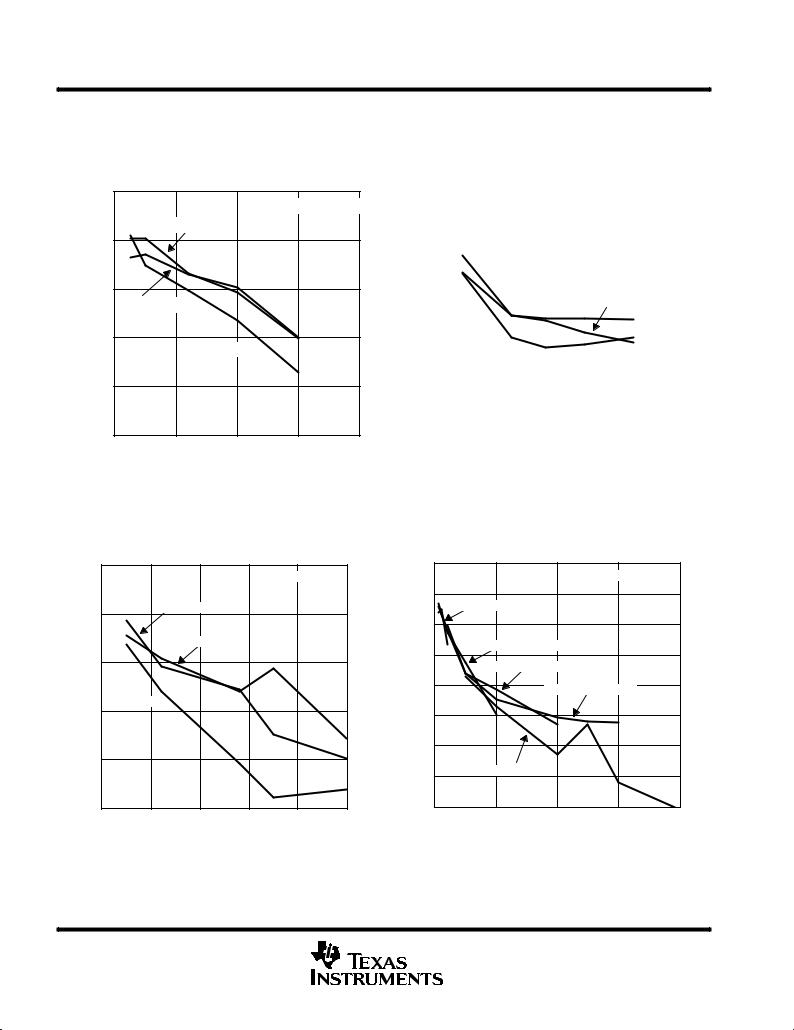
TYPICAL CHARACTERISTICS²
SPURIOUS FREE DYNAMIC RANGE vs
OUTPUT FREQUENCY AT 70 MSPS
78
DVDD = 5 V
± 6 dBFS
|
72 |
dBc |
66 |
|
|
SFDR ± |
± 12 dBFS |
60 |
0 dBFS
54
48
0 |
10 |
20 |
30 |
40 |
|
Fout ± Output Frequency ± MHz |
|
||
Figure 5
SPURIOUS FREE DYNAMIC RANGE vs
OUTPUT FREQUENCY AT 125 MSPS
|
78 |
|
|
|
DVDD = 5 V |
|
|
|
|
|
|
|
|
|
72 |
|
± 6 dBFS |
|
|
|
|
|
|
|
|
|
|
|
|
|
± 12 dBFS |
|
|
|
± dBc |
66 |
|
|
|
|
|
|
|
|
|
|
|
|
SFDR |
60 |
0 dBFS |
|
|
|
|
|
|
|
|
|
||
|
54 |
|
|
|
|
|
|
48 |
|
|
|
|
|
|
0 |
10 |
20 |
30 |
40 |
50 |
|
|
Fout ± Output Frequency ± MHz |
|
|||
Figure 7
|
|
|
SPURIOUS FREE DYNAMIC RANGE |
|
|
||||||||||||
|
|
|
|
|
|
|
|
|
vs |
|
|
|
|
|
|||
|
|
|
OUTPUT FREQUENCY AT 100 MSPS |
|
|
||||||||||||
|
78 |
|
|
|
|
|
|
|
|
|
|
|
|
|
|
|
|
|
|
|
|
|
|
|
|
|
|
|
|
|
DVDD = 5 V |
|
|
||
|
72 |
|
|
|
|
|
|
|
|
|
|
|
|
|
|
|
|
|
|
|
|
|
|
|
|
|
|
|
|
|
|
|
|
|
|
|
|
|
|
|
|
|
|
|
|
|
|
|
|
|
|
|
|
|
|
|
|
± 6 dBFS |
|
|
|
|
|
|
|
|
|
|
|
|
|
dBc |
66 |
|
|
|
|
|
|
|
|
|
± 12 dBFS |
|
|
|
|
||
|
|
|
|
|
|
|
|
|
|
|
|
|
|||||
SFDR ± |
|
|
|
|
|
|
|
|
|
|
|
|
|
|
|
|
|
60 |
|
|
|
|
|
|
|
|
|
|
|
|
|
|
|
|
|
|
|
|
|
|
|
|
|
|
|
|
|
|
|
|
|
||
|
|
|
|
|
|
|
|
|
|
|
|
|
|
|
|
||
|
|
|
|
|
|
|
|
|
|
|
|
|
|
|
|
|
|
|
|
|
|
|
|
|
|
|
0 dBFS |
|
|
|
|
|
|
|
|
|
54 |
|
|
|
|
|
|
|
|
|
|
|
|
|
|
|
|
|
|
|
|
|
|
|
|
|
|
|
|
|
|
|
|
|
|
|
|
|
|
|
|
|
|
|
|
|
|
|
|
|
|
|
|
|
48 |
|
|
|
|
|
|
|
|
|
|
|
|
|
|
|
|
|
|
|
|
|
|
|
|
|
|
|
|
|
|
|
|
|
|
|
0 |
10 |
20 |
30 |
40 |
|
50 |
||||||||||
Fout ± Output Frequency ± MHz
Figure 6
SPURIOUS FREE DYNAMIC RANGE vs
OUTPUT FREQUENCY AT 0 dBFS
|
90 |
|
|
DVDD = 3.3 V |
|
|
|
|
|
|
|
|
84 |
fCLK = 5 MSPS |
|
|
|
|
|
|
|
|
|
|
78 |
|
|
|
|
|
72 |
fCLK = 25 MSPS |
|
|
|
dBc |
|
|
|
|
|
|
fCLK = 50 MSPS |
|
|
||
± |
66 |
|
fCLK = 70 MSPS |
|
|
SFDR |
|
|
|||
|
|
|
|||
60 |
|
|
|
|
|
|
|
|
|
|
|
|
54 |
|
|
|
|
|
48 |
fCLK = 100 MSPS |
|
|
|
|
|
|
|
|
|
|
42 |
|
|
|
|
|
0 |
10 |
20 |
30 |
40 |
|
|
Fout ± Output Frequency ± MHz |
|
||
Figure 8
²AV DD = 5 V, IOUTFS = 20 mA, differential transformer coupled output, 50 Ω doubly terminated load, TA = 25°C (unless otherwise noted.)
8 |
POST OFFICE BOX 655303 •DALLAS, TEXAS 75265 |
THS5661A 12-BIT, 125 MSPS, CommsDAC
DIGITAL-TO-ANALOG CONVERTER
SLAS247 ± NOVEMBER 1999
TYPICAL CHARACTERISTICS²
|
|
|
SPURIOUS FREE DYNAMIC RANGE |
|
|
||||||||
|
|
|
|
|
|
|
|
vs |
|
|
|
|
|
|
|
|
OUTPUT FREQUENCY AT 5 MSPS |
|
|
||||||||
|
90 |
|
|
|
|
|
|
|
|
|
|
|
|
|
|
|
|
|
|
|
|
|
|
|
|
|
|
|
|
|
|
|
|
|
|
|
|
DVDD = |
3.3 V |
|
|
|
84 |
|
|
|
|
|
|
|
|
|
|
|
|
|
|
|
|
|
|
|
|
|
|
|
|
|
|
|
|
|
|
|
|
|
|
|
|
|
|
|
|
|
|
|
0 dBFS |
|
|
|
|
|
|
|
|
|
|
dBc± |
78 |
|
|
|
± 6 dBFS |
|
|
|
|
|
|
|
|
SFDR |
|
|
|
|
|
|
|
|
|
|
|
|
|
72 |
|
|
|
|
|
|
|
|
|
|
|
|
|
|
|
|
|
|
|
|
|
|
|
|
|
||
|
|
|
|
|
|
|
|
|
|
|
|
||
|
|
|
|
|
|
|
|
|
|
|
|
||
|
|
|
± 12 dBFS |
|
|
|
|
|
|
|
|
||
|
66 |
|
|
|
|
|
|
|
|
|
|
|
|
|
|
|
|
|
|
|
|
|
|
|
|
|
|
|
60 |
|
|
|
|
|
|
|
|
|
|
|
|
|
|
|
|
|
|
|
|
|
|
|
|
|
|
|
0 |
0.5 |
1.0 |
1.5 |
2.0 |
2.5 |
|||||||
Fout ± Output Frequency ± MHz
Figure 9
SPURIOUS FREE DYNAMIC RANGE vs
OUTPUT FREQUENCY AT 50 MSPS
|
78 |
|
|
|
|
|
|
|
|
|
|
DVDD = 3.3 V |
|
|
|
0 dBFS |
|
|
|
|
|
72 |
|
± 6 dBFS |
|
|
|
|
|
|
|
|
|
|
± dBc |
66 |
± 12 dBFS |
|
|
|
|
|
|
|
|
|
||
|
|
|
|
|
|
|
SFDR |
60 |
|
|
|
|
|
|
|
|
|
|
|
|
|
54 |
|
|
|
|
|
|
48 |
|
|
|
|
|
|
0 |
5 |
10 |
15 |
20 |
25 |
|
|
Fout ± Output Frequency ± MHz |
|
|||
Figure 11
SFDR ± dBc
SFDR ± dBc
SPURIOUS FREE DYNAMIC RANGE vs
OUTPUT FREQUENCY AT 25 MSPS
90 |
|
|
|
|
|
|
|
|
|
|
|
|
|
|
|
|
|
|
|
|
|
|
|
|
|
|
|
|
|
|
|
|
|
|
|
|
|
|
|
|
|
|
|
DVDD = 3.3 V |
|
|
|
|||
84 |
|
|
|
|
|
|
|
|
|
|
|
|
|
|
|
|
|
|
|
|
|
|
|
|
|
|
|
|
|
|
|
|
|
|
|
|
|
|
|
|
|
|
|
|
|
|
|
|
|
|
|
|
|
|
0 dBFS |
|
|
|
|
|
|
|
|
|
|
|
|
78 |
|
|
|
|
|
|
|
|
|
|
|
|
|
|
|
|
|
|
|
|
|
|
|
|
|
|
|
|
|
|
|
|
|
72 |
|
|
|
|
|
|
|
|
|
|
|
|
|
|
|
|
|
|
|
|
|
|
|
|
|
|
|
|
|
|
|
|
|
|
|
|
|
|
|
|
|
|
|
|
|
|
|
|
|
|
|
|
± 12 dBFS |
|
|
|
|
|
|
|
|
|
|
|
|
||
|
|
|
|
|
|
|
|
|
|
|
|
|
|
|
|
|
66 |
|
|
|
|
|
|
|
|
|
|
|
± 6 |
dBFS |
|
|
|
60 |
|
|
|
|
|
|
|
|
|
|
|
|
|
|
|
|
|
|
|
|
|
|
|
|
|
|
|
|
|
|
|
|
|
0 |
2 |
|
4 |
6 |
8 |
10 |
12 |
|||||||||
Fout ± Output Frequency ± MHz
Figure 10
SPURIOUS FREE DYNAMIC RANGE vs
OUTPUT FREQUENCY AT 70 MSPS
78
DVDD = 3.3 V
72
± 6 dBFS
66
0 dBFS
60
± 12 dBFS
54
48
0 |
10 |
20 |
30 |
40 |
|
Fout ± Output Frequency ± MHz |
|
||
Figure 12
²AV DD = 5 V, IOUTFS = 20 mA, differential transformer coupled output, 50 Ω doubly terminated load, TA = 25°C (unless otherwise noted.)
POST OFFICE BOX 655303 •DALLAS, TEXAS 75265 |
9 |

THS5661A
12-BIT, 125 MSPS, CommsDAC
DIGITAL-TO-ANALOG CONVERTER
SLAS247 ± NOVEMBER 1999
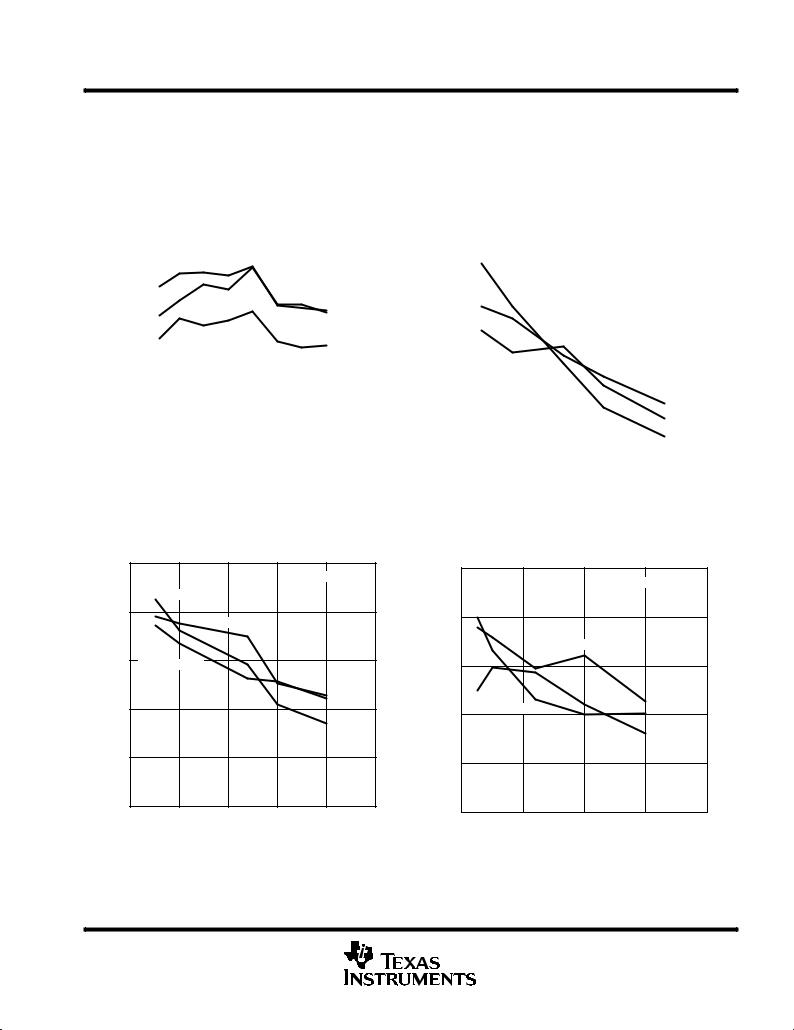
TYPICAL CHARACTERISTICS²
SPURIOUS FREE DYNAMIC RANGE
|
|
|
|
|
vs |
|
|
|
|
|
|
|
|
AOUT AT FOUT = FCLOCK/11 |
|
|
|||||
|
78 |
|
|
|
|
|
|
DVDD = 5 V |
|
|
|
|
|
|
|
|
|
|
|
||
|
|
4.55 MHz @ 50 MSPS |
|
|
|
|
||||
|
72 |
|
|
|
|
|
|
|
|
|
dBc |
66 |
|
|
|
|
|
|
|
|
|
|
|
|
6.36 MHz @ 70 MSPS |
|
|
|||||
± |
|
|
|
|
|
|||||
|
|
|
|
|
|
|
|
|
|
|
SFDR |
60 |
|
|
|
|
|
|
|
|
|
|
|
|
|
|
|
|
|
|
|
|
|
|
|
9.1 MHz @ 100 MSPS |
|
|
|
|
|||
|
54 |
|
|
|
|
|
|
|
|
|
|
48 |
|
|
|
|
|
|
|
|
|
|
±27 |
±24 |
±21 |
±18 |
±15 |
±12 |
±9 |
±6 |
±3 |
0 |
|
|
|
|
|
Aout ± dBFS |
|
|
|
|
|
Figure 13
DUAL TONE SPURIOUS FREE DYNAMIC RANGE
|
|
|
|
|
vs |
|
|
|
|
|
|
|
|
AOUT AT FOUT = FCLOCK/7 |
|
|
|||||
|
78 |
|
|
|
|
|
|
|
|
|
|
|
|
|
|
|
|
|
DVDD = 5 V |
|
|
|
72 |
0.675/0.725 MHz @ 5 MSPS |
|
|
|
|
||||
|
|
|
|
|
|
|
|
|
|
|
|
3.38/3.63 MHz @ 25 MSPS |
|
|
|
|
|||||
± dBc |
66 |
|
|
|
|
|
|
|
|
|
|
|
|
|
|
|
|
|
|
|
|
SFDR |
60 |
|
|
|
|
|
|
|
|
|
|
|
|
|
|
|
|
|
|
|
|
|
|
|
|
|
|
|
13.5/14.5 MHz |
|
||
|
54 |
|
|
|
|
|
@ 100 MSPS |
|
||
|
|
|
|
|
6.75/7.25 MHz @ 50 MSPS |
|
||||
|
48 |
|
|
9.67/10.43 MHz @ 70 MSPS |
|
|
||||
|
|
|
|
|
|
|
|
|
|
|
|
±27 |
±24 |
±21 |
±18 |
±15 |
±12 |
±9 |
±6 |
±3 |
0 |
|
|
|
|
|
Aout ± dBFS |
|
|
|
|
|
Figure 15
SPURIOUS FREE DYNAMIC RANGE
|
|
|
|
|
vs |
|
|
|
|
|
|
|
|
AOUT AT FOUT = FCLOCK/5 |
|
|
|||||
|
78 |
|
|
|
|
|
|
DVDD = 5 V |
|
|
|
|
|
|
|
|
|
|
|
||
|
72 |
|
|
|
|
5 MHz @ 25 MSPS |
|
|||
|
|
|
|
|
|
|
||||
|
66 |
|
|
|
|
|
|
|
|
|
± dBc |
|
10 MHz @ 50 MSPS |
|
|
|
|
|
|||
60 |
|
|
|
|
|
|
|
|
|
|
SFDR |
54 |
|
|
|
|
|
|
|
|
|
|
|
|
|
|
|
|
|
|
|
|
|
48 |
|
|
|
|
14 MHz @ 70 MSPS |
|
|||
|
|
|
|
|
|
|
||||
|
42 |
|
|
|
20 MHz @ 100 MSPS |
|
|
|||
|
|
|
|
|
|
|
|
|
|
|
|
±27 |
±24 |
±21 |
±18 |
±15 |
±12 |
±9 |
±6 |
±3 |
0 |
Aout ± dBFS
Figure 14
TOTAL HARMONIC DISTORTION vs
CLOCK FREQUENCY AT FOUT = 2 MHz
±66 |
|
|
|
|
|
|
|
|
|
|
|
DVDD = 5 V |
|
±72 |
2nd Harmonic |
|
|
|
|
|
|
|
|
|
|
||
±dBc |
|
|
|
|
|
|
±78 |
|
|
|
|
|
|
THD |
|
|
|
3rd Harmonic |
|
|
|
|
|
|
|
|
|
±84 |
4th Harmonic |
|
|
|
|
|
|
|
|
|
|
||
±90 |
|
|
|
|
|
|
0 |
20 |
40 |
60 |
80 |
100 |
120 |
|
Fclock ±Clock Frequency ± MSPS |
|
||||
Figure 16
²AV DD = 5 V, IOUTFS = 20 mA, differential transformer coupled output, 50 Ω doubly terminated load, TA = 25°C (unless otherwise noted.)
10 |
POST OFFICE BOX 655303 •DALLAS, TEXAS 75265 |
 Loading...