


THS4031
THS4032
"THS4031M"
www.ti.com |
SLOS224G –JULY 1999 –REVISED MARCH 2010 |
100-MHz LOW-NOISE HIGH-SPEED AMPLIFIERS
Check for Samples: THS4031, THS4032
FEATURES
•Ultralow 1.6 nV/√Hz Voltage Noise
•High Speed:
–100-MHz Bandwidth [G = 2 (-1), –3 dB]
–100-V/ms Slew Rate
•Very Low Distortion
–THD = –72 dBc (f = 1 MHz, RL = 150 Ω)
–THD = –90 dBc (f = 1 MHz, RL = 1 kΩ)
•Low 0.5-mV (Typ) Input Offset Voltage
•90-mA Output Current Drive (Typical)
•± 5 V to ± 15 V Typical Operation
•Available in Standard SOIC, MSOP PowerPAD™ , JG, or FK Package
•Evaluation Module Available
DESCRIPTION
The THS4031 and THS4032 are ultralow-voltage noise, high-speed voltage feedback amplifiers that are ideal for applications requiring low voltage noise, including communications and imaging. The single amplifier THS4031 and the dual amplifier THS4032 offer very good ac performance with 100-MHz bandwidth (G = 2), 100-V/ms slew rate, and 60-ns settling time (0.1%). The THS4031 and THS4032 are unity gain stable with 275-MHz bandwidth. These amplifiers have a high drive capability of 90 mA and draw only 8.5-mA supply current per channel. With –90 dBc of total harmonic distortion (THD) at f = 1 MHz and a very low noise of 1.6 nV/√Hz, the THS4031 and THS4032 are ideally suited for applications requiring low distortion and low noise such as buffering analog-to-digital converters.
|
RELATED DEVICES |
DEVICE |
DESCRIPTION |
|
|
THS4051/2 |
70-MHz High-Speed Amplifiers |
|
|
THS4081/2 |
175-MHz Low Power High-Speed Amplifiers |
|
|
THS4031
D, DGN, AND JG PACKAGE
(TOP VIEW)
NULL |
|
|
1 |
|
|
|
8 |
|
|
NULL |
|||||
|
|
|
|
|
|
|
|||||||||
|
|
|
|
|
|
|
|||||||||
IN− |
|
|
2 |
|
|
|
|
|
|
|
7 |
|
|
VCC+ |
|
|
|
|
|
|
|
|
|
|
|
|
|||||
IN+ |
|
|
3 |
|
|
|
|
|
|
|
6 |
|
|
OUT |
|
VCC− |
|
4 |
|
|
|
5 |
|
|
NC |
||||||
|
|
|
|
|
|
|
|||||||||
|
|
|
|
|
|
|
|||||||||
NC − No internal connection
THS4032
D AND DGN PACKAGE
(TOP VIEW)
1OUT |
|
|
1 |
|
|
|
|
|
8 |
|
|
|
VCC+ |
|||||||||||||
|
|
|
|
|
|
|
|
|
|
|
||||||||||||||||
|
|
|
|
|
||||||||||||||||||||||
1IN− |
|
|
|
2 |
|
|
|
|
|
|
|
|
|
|
|
|
|
|
7 |
|
|
|
2OUT |
|||
1IN+ |
|
|
3 |
|
|
|
|
|
|
|
|
|
|
|
|
|
|
6 |
|
|
|
2IN− |
||||
−V CC |
|
|
4 |
|
|
|
|
|
|
|
|
|
5 |
|
|
|
2IN+ |
|||||||||
|
|
|
|
|
|
|
|
|
|
|
|
|
|
|
||||||||||||
|
|
|
|
|
|
|
||||||||||||||||||||
|
|
|
|
|
|
|
|
|
|
|
|
|
|
|
|
|
|
|
|
|
|
|
|
|
|
|
|
|
|
|
|
|
|
|
|
|
|
|
|
|
|
|
|
|
|
|
|
|
|
|
|
|
|
|
|
|
|
|
|
|
|
|
|
|
|
|
|
|
|
|
|
|
|
|
|
|
|
|
|
|
|
|
|
|
|
|
|
|
|
|
|
|
|
|
|
|
|
|
|
|
|
|
|
|
|
|
|
|
|
|
|
|
|
|
|
|
|
|
|
|
|
|
|
|
|
|
|
|
|
|
|
|
|
|
Cross-Section View Showing
PowerPAD Option (DGN)
THS4031
FK PACKAGE (TOP VIEW)
|
NC |
NULL |
NC |
NULL |
NC |
|
|
3 |
2 |
1 |
20 |
19 |
|
NC |
4 |
|
|
|
18 |
NC |
IN− |
5 |
|
|
|
17 |
VCC+ |
NC |
6 |
|
|
|
16 |
NC |
IN+ |
7 |
|
|
|
15 |
OUT |
NC |
8 |
|
|
|
14 |
NC |
|
9 |
10 |
11 |
12 |
13 |
|
|
NC |
CC− |
NC |
NC |
NC |
|
|
|
V |
|
|
|
|
Please be aware that an important notice concerning availability, standard warranty, and use in critical applications of Texas Instruments semiconductor products and disclaimers thereto appears at the end of this data sheet.
PowerPAD is a trademark of Texas Instruments.
PRODUCTION DATA information is current as of publication date. |
Copyright © 1999–2010, Texas Instruments Incorporated |
Products conform to specifications per the terms of the Texas |
|
Instruments standard warranty. Production processing does not |
|
necessarily include testing of all parameters. |
|

THS4031
THS4032
SLOS224G –JULY 1999 –REVISED MARCH 2010 |
www.ti.com |
||
|
"THS4031M" |
|
|
These devices have limited built-in ESD protection. The leads should be shorted together or the device placed in conductive foam during storage or handling to prevent electrostatic damage to the MOS gates.
VOLTAGE NOISE AND CURRENT NOISE
|
|
|
|
vs |
|
|
|
|
|
|
FREQUENCY |
|
|
|
|
20 |
|
|
|
|
|
|
|
|
VCC = ± 15 V AND ± 5 V |
|
|
|
|
|
|
TA = 25°C |
|
|
Hz |
Hz |
10 |
|
|
|
|
|
|
|
|
|
||
nV/ |
pA/ |
|
|
|
|
|
V oltage Noise − |
Current Noise − |
|
|
|
|
|
− |
− |
|
|
|
|
|
n |
n |
|
|
Vn |
|
|
V |
I |
|
|
|
|
|
|
|
|
|
In |
|
|
|
|
1 |
|
|
|
|
|
|
10 |
100 |
1 k |
10 k |
100 k |
|
|
|
|
f − Frequency − Hz |
|
|
AVAILABLE OPTIONS(1)
|
|
|
|
|
PACKAGED DEVICES |
|
|
|||
|
NUMBER OF |
|
|
|
|
|
|
EVALUATION |
||
TA |
PLASTIC |
|
PLASTIC MSOP(2)(DGN)(3) |
CERAMIC DIP |
CHIP CARRIER |
|||||
CHANNELS |
SMALL |
|
|
|
MODULE |
|||||
|
|
DEVICE |
SYMBOL |
(JG) |
(FK) |
|||||
|
|
OUTLINE |
(2) |
(D) |
|
|||||
|
|
|
|
|
|
|
|
|||
|
|
|
|
|
|
|
|
|||
0°C to 70°C |
1 |
THS4031CD |
THS4031CDGN |
TIACM |
— |
— |
THS4031EVM |
|||
|
|
|
|
|
|
|
|
|
||
2 |
THS4032CD |
THS4032CDGN |
TIABD |
— |
— |
THS4032EVM |
||||
|
||||||||||
|
|
|
|
|
|
|
|
|||
–40°C to 85°C |
1 |
THS4031ID |
THS4031IDGN |
TIACN |
— |
— |
— |
|||
|
|
|
|
|
|
|
|
|
||
2 |
THS4032ID |
THS4032IDGN |
TIABG |
— |
— |
— |
||||
|
||||||||||
|
|
|
|
|
|
|
|
|
|
|
–55°C to 125°C |
1 |
— |
|
|
— |
— |
THS4031MJG |
THS4031MFK |
— |
|
|
|
|
|
|
|
|
|
|
|
|
(1)For the most current package and ordering information, see the Package Option Addendum at the end of this document, or see the TI web site at www.ti.com.
(2)The D and DGN packages are available taped and reeled. Add an R suffix to the device type (that is, THS4031CDGNR).
(3) The PowerPAD™ on the underside of the DGN package is electrically isolated from all other pins and active circuitry. Connection to the PCB ground plane is recommended, although not required, as this copper plane is typically the largest copper plane on the PCB.
2 |
Submit Documentation Feedback |
Copyright © 1999–2010, Texas Instruments Incorporated |
Product Folder Link(s): THS4031 THS4032

|
|
|
|
|
|
|
|
|
|
|
|
|
|
|
|
|
|
|
|
THS4031 |
|
|
|
|
|
|
|
|
|
|
|
|
|
|
|
|
|
|
|
|
|
THS4032 |
|
www.ti.com |
|
|
|
|
|
|
|
|
|
|
|
|
SLOS224G –JULY 1999 –REVISED MARCH 2010 |
||||||||
|
"THS4031M" |
|
|
|
|
|
|
|
|
|
|
|
|
|
|
|
|||||
FUNCTIONAL BLOCK DIAGRAMS |
|
|
|
|
|
|
|
|
|
|
|||||||||||
|
|
|
|
|
Null |
|
|
|
|
|
|
|
|
|
VCC |
|
|
||||
|
|
|
1 |
|
|
|
|
|
|
|
2 |
|
|
|
|
8 |
|
|
|
||
|
IN− |
2 |
|
|
8 |
|
|
1IN− |
|
|
− |
|
|
|
|
||||||
|
|
|
|
|
|
|
|
|
|
|
|
|
|||||||||
|
|
|
|
|
|
|
|
|
|
|
|
||||||||||
|
|
|
− |
|
6 |
OUT |
|
3 |
|
|
|
|
|
1 |
1OUT |
||||||
|
|
|
|
|
|
|
|
|
|
|
|
|
|
||||||||
|
|
|
|
|
|
|
|
|
|
|
|
|
|
|
|||||||
|
|
|
|
|
|
|
|
|
|
|
|
|
|
|
|
|
|
||||
|
IN+ |
3 |
+ |
|
|
|
|
|
|
1IN+ |
|
|
+ |
|
|
|
|
|
|||
|
|
|
|
|
|
|
|
|
|
|
|
|
|
|
|||||||
|
|
|
|
|
|
|
|
|
|
|
|
|
|
|
|
||||||
|
|
|
|
|
|
|
|
|
|
|
|
|
|
|
|
|
|
||||
|
|
|
|
|
|
|
|
|
|
2IN− |
6 |
|
|
− |
|
|
|
|
|
||
|
|
|
|
|
|
|
|
|
|
|
|
|
|
|
|
|
|
|
|||
|
|
|
|
|
|
|
|
|
|
|
|
|
|
|
|
|
|
|
|||
|
|
|
|
|
|
|
|
|
|
|
|
|
|
|
|
|
|
|
|||
|
|
|
|
|
|
|
|
|
|
|
|
|
|
|
7 |
2OUT |
|||||
|
|
|
|
|
|
|
|
|
|
|
|
|
|
|
|
|
|||||
|
|
|
|
|
|
|
|
|
|
|
|
2IN+ |
5 |
|
|
+ |
|
|
|
||
|
|
|
|
|
|
|
|
|
|
|
|
|
|
|
|
|
|
|
|||
|
|
|
|
|
|
|
|
|
|
|
|
|
|
|
|
4 |
|
|
|
||
|
|
|
|
|
|
|
|
|
|
|
|
|
|
|
|
|
|
|
|
|
|
|
|
|
|
|
|
|
|
|
|
|
|
|
|
|
|
|
|
|
|
|
|
|
|
|
|
|
|
|
|
|
|
|
|
|
|
|
|
|
|
|
|
|
|
|
|
|
|
|
|
|
|
|
|
|
|
|
|
|
|
|
−V CC |
|
|
||
|
Figure 1. THS4031 – Single Channel |
Figure 2. THS4032 – Dual Channel |
|||||||||||||||||||
ABSOLUTE MAXIMUM RATINGS(1) |
|
|
|
|
|
|
|
|
|
|
|||||||||||
Over operating free-air temperature range (unless otherwise noted). |
|
|
|
|
|
|
|
|
|
|
|||||||||||
|
|
|
|
|
|
|
|
|
|
|
|
|
|
|
|
|
|
|
|
|
|
|
|
|
|
|
|
|
|
|
|
|
|
|
|
|
|
|
|
VALUE |
|
UNIT |
|
|
|
|
|
|
|
|
|
|
|
|
|
||||||||||
VCC |
Supply voltage, VCC+ to VCC– |
|
|
|
|
|
33 |
|
V |
||||||||||||
VI |
Input voltage |
|
|
|
|
|
|
|
|
|
|
|
±VCC |
|
|
||||||
IO |
Output current |
|
|
|
|
|
|
|
|
|
150 |
|
mA |
||||||||
VIO |
Differential input voltage |
|
|
|
|
|
±4 |
|
V |
||||||||||||
|
|
Continuous total power dissipation |
|
|
|
|
|
See Dissipation Ratings Table |
|||||||||||||
|
|
|
|
|
|
|
|
|
|
|
|
|
|
|
|
|
|
|
|||
|
|
Operating free-air |
|
C-suffix |
|
|
|
|
|
|
0 to 70 |
|
|
||||||||
|
|
|
|
|
|
|
|
|
|
|
|
|
|
|
|
||||||
TA |
|
I-suffix |
|
|
|
|
|
|
–40 to 85 |
|
°C |
||||||||||
temperature |
|
|
|
|
|
|
|
|
|||||||||||||
|
|
|
M-suffix |
|
|
|
|
|
|
–55 to 125 |
|
|
|||||||||
|
|
|
|
|
|
|
|
|
|
|
|
|
|
|
|
|
|||||
|
|
|
|
|
|
|
|
|
|
|
|
|
|||||||||
TJ |
Maximum junction temperature, (any condition) |
|
|
|
|
|
150 |
|
°C |
||||||||||||
|
|
Maximum junction temperature, continuous operation, long term reliability(2) |
|
|
|
130 |
|
°C |
|||||||||||||
Tstg |
Storage temperature |
|
|
|
|
|
|
|
|
|
|
–65 to 150 |
|
°C |
|||||||
|
|
Lead temperature 1,6 mm (1/16 inch) from case for 10 seconds |
|
|
|
|
|
300 |
|
°C |
|||||||||||
|
|
|
|
|
|
|
|
|
|
|
|||||||||||
|
|
Lead temperature 1,6 mm (1/16 inch) from case for 60 seconds, JG package |
|
|
|
300 |
|
°C |
|||||||||||||
|
|
|
|
|
|
|
|
|
|
|
|
|
|||||||||
|
|
Case temperature for 60 seconds, FK package |
|
|
|
|
|
260 |
|
°C |
|||||||||||
|
|
|
|
|
|
|
|
|
|
|
|
|
|
|
|
|
|
|
|
|
|
(1)Stresses beyond those listed under absolute maximum ratings may cause permanent damage to the device. These are stress ratings only and functional operation of the device at these or any other conditions beyond those indicated under recommended operating conditions is not implied. Exposure to absolute-maximum-rated conditions for extended periods may affect device reliability.
(2)The maximum junction temperature for continuous operation is limited by package constraints. Operation above this temperature may result in reduced reliability and/or lifetime of the device. Does not apply to the JG package or FK package.
DISSIPATION RATINGS TABLE
PACKAGE |
qJA |
qJC |
TA = 25°C, |
|
(°C/W) |
(°C/W) |
POWER RATING |
D |
167(1) |
38.3 |
629 mW, T = 130°C, continuous |
|
|
|
J |
DGN(2) |
58.4 |
4.7 |
1.8 W, T = 130°C, continuous |
|
|
|
J |
JG |
119 |
28 |
1050 mW, TJ = 150°C, continuous |
FK |
87.7 |
20 |
1375 mW, TJ = 150°C, continuous |
(1)This data was taken using the JEDEC standard Low-K test PCB. For the JEDEC Proposed High-K test PCB, the qJA is 95°C/W with a power rating at TA = 25°C of 1.32 W.
(2)This data was taken using 2 oz. trace and copper pad that is soldered directly to a 3-in. × 3-in. PC. For further information, refer to Application Information section of this data sheet.
Copyright © 1999–2010, Texas Instruments Incorporated |
Submit Documentation Feedback |
3 |
Product Folder Link(s): THS4031 THS4032

THS4031
THS4032
SLOS224G –JULY 1999 –REVISED MARCH 2010 |
|
www.ti.com |
||||||
|
"THS4031M" |
|
|
|
|
|
||
RECOMMENDED OPERATING CONDITIONS |
|
|
|
|||||
|
|
|
|
|
MIN NOM |
MAX |
UNIT |
|
|
|
|
|
|
|
|
|
|
VCC+ and VCC– |
Supply voltage |
Dual supply |
±4.5 |
±16 |
V |
|||
|
|
|
||||||
Single supply |
9 |
32 |
||||||
|
|
|
|
|
||||
|
|
|
|
|
|
|
|
|
|
|
Operating free-air |
C-suffix |
0 |
70 |
|
||
|
|
|
|
|
|
|||
TA |
I-suffix |
–40 |
85 |
°C |
||||
temperature |
||||||||
|
|
M-suffix |
–55 |
125 |
|
|||
|
|
|
|
|
||||
|
|
|
|
|
|
|
|
|
ELECTRICAL CHARACTERISTICS
At TA = 25°C, VCC = ±15 V, and RL = 150 Ω (unless otherwise noted).
|
PARAMETER |
TEST CONDITIONS(1) |
|
THS403xC, THS403xI |
UNIT |
|||||||
|
|
|
|
|
||||||||
|
|
MIN |
TYP |
MAX |
||||||||
|
|
|
|
|
|
|
||||||
|
|
|
|
|
|
|
|
|
|
|
||
DYNAMIC PERFORMANCE |
|
|
|
|
|
|
|
|
|
|
||
|
|
|
|
|
|
|
|
|
|
|
|
|
|
Small-signal bandwidth (–3 dB) |
VCC = ±15 V |
|
Gain = –1 or 2 |
|
100 |
|
MHz |
||||
|
VCC = ±5 V |
|
|
90 |
|
|||||||
|
|
|
|
|
|
|
|
|
|
|
||
BW |
Bandwidth for 0.1-dB flatness |
VCC = ±15 V |
|
Gain = –1 or 2 |
|
50 |
|
MHz |
||||
VCC = ±5 V |
|
|
45 |
|
||||||||
|
|
|
|
|
|
|
|
|
|
|
||
|
Full power bandwidth(2) |
VO(pp) = 20 V, |
VCC = ±15 V |
RL = 1 kΩ |
|
2.3 |
|
MHz |
||||
|
VO(pp) = 5 V, |
VCC = ±5 V |
|
7.2 |
|
|||||||
|
|
|
|
|
|
|
|
|
|
|||
SR |
Slew rate(3) |
VCC = ±15 V, |
20-V step |
Gain = –1 |
|
100 |
|
V/ms |
||||
VCC = ±5 V, |
5-V step |
|
80 |
|
||||||||
|
|
|
|
|
|
|
|
|
|
|||
|
Settling time to 0.1% |
VCC = ±15 V, |
5-V step |
Gain = –1 |
|
60 |
|
ns |
||||
tS |
VCC = ±5 V, |
2.5-V step |
|
45 |
|
|||||||
|
|
|
|
|
|
|
|
|
||||
Settling time to 0.01% |
VCC = ±15 V, |
5-V step |
Gain = –1 |
|
90 |
|
ns |
|||||
|
|
|
||||||||||
|
VCC = ±5 V, |
2.5-V step |
|
80 |
|
|||||||
|
|
|
|
|
|
|
|
|
|
|||
NOISE/DISTORTION PERFORMANCE |
|
|
|
|
|
|
|
|
|
|
||
|
|
|
|
|
|
|
|
|
|
|
|
|
|
|
THS4031 |
|
|
RL = 150 Ω |
|
–81 |
|
|
|
|
|
THD |
Total harmonic |
VCC = ±5 V or ±15 V, |
VO(pp) = 2 V, |
RL = 1 kΩ |
|
–96 |
|
dBc |
||||
|
|
|
||||||||||
|
RL = 150 Ω |
|
|
|
||||||||
|
distortion |
THS4032 |
f = 1 MHz |
Gain = 2 |
|
–72 |
|
|
|
|
|
|
|
|
|
|
RL = 1 kΩ |
|
–90 |
|
|
|
|
|
|
|
|
|
|
|
|
|
|
|
|
|
||
Vn |
Input voltage noise |
VCC = ±5 V or ±15 V, |
f > 10 kHz |
|
|
1.6 |
|
nV/√ |
|
|
||
|
|
|
Hz |
|||||||||
In |
Input current noise |
VCC = ±5 V or ±15 V, |
f > 10 kHz |
|
|
1.2 |
|
pA/√ |
|
|
|
|
|
|
|
Hz |
|||||||||
|
Differential gain error |
|
|
VCC = ±15 V |
|
0.015% |
|
|
|
|
|
|
|
Gain = 2, |
NTSC and PAL, |
VCC = ±5 V |
|
0.02% |
|
|
|
|
|
||
|
|
|
|
|
|
|
|
|
||||
|
Differential phase error |
40 IRE modulation, |
±100 IRE ramp |
VCC = ±15 V |
|
0.025 |
|
° |
|
|
|
|
|
|
|
VCC = ±5 V |
|
0.03 |
|
|
|
|
|||
|
|
|
|
|
|
|
|
|
|
|
||
|
Channel-to-channel crosstalk |
VCC = ±5 V or ±15 V, |
f = 1 MHz |
|
|
–61 |
|
dBc |
||||
|
(THS4032 only) |
|
|
|
||||||||
(1)Full range = 0°C to 70°C for THS403xC and –40°C to 85°C for THS403xI suffix.
(2)Full power bandwidth = slew rate / [√2 pVOC(Peak)].
(3)Slew rate is measured from an output level range of 25% to 75%.
4 |
Submit Documentation Feedback |
Copyright © 1999–2010, Texas Instruments Incorporated |
Product Folder Link(s): THS4031 THS4032

|
|
|
|
|
|
|
|
|
|
THS4031 |
|
|
|
|
|
|
|
|
|
|
|
THS4032 |
|
www.ti.com |
|
|
|
SLOS224G –JULY 1999 –REVISED MARCH 2010 |
|||||||
|
"THS4031M" |
|
|
|
|
|
|
|
|
|
|
ELECTRICAL CHARACTERISTICS (continued) |
|
|
|
|
|
|
|||||
At TA = 25°C, VCC = ±15 V, and RL = 150 Ω (unless otherwise noted). |
|
|
|
|
|||||||
|
|
PARAMETER |
|
TEST CONDITIONS(1) |
THS403xC, THS403xI |
UNIT |
|||||
|
|
|
|
|
|
||||||
|
|
|
MIN |
TYP |
MAX |
||||||
|
|
|
|
|
|
|
|
|
|||
|
|
|
|
|
|
|
|
|
|
|
|
DC PERFORMANCE |
|
|
|
|
|
|
|
|
|||
|
|
|
|
|
|
|
|
|
|
|
|
|
|
|
|
VCC |
= ±15 V, RL = 1 kΩ, VO = ±10 V |
TA = 25°C |
93 |
98 |
|
|
|
|
|
Open loop gain |
TA = full range |
92 |
|
|
dB |
||||
|
|
|
|
|
|
|
|||||
|
|
VCC |
= ±5 V, RL = 1 kΩ, VO |
= ±2.5 V |
TA = 25°C |
90 |
95 |
|
|||
|
|
|
|
|
|
||||||
|
|
|
|
TA = full range |
89 |
|
|
|
|||
|
|
|
|
|
|
|
|
|
|
||
VOS |
Input offset voltage |
VCC |
= ±5 V or ±15 V |
|
TA = 25°C |
|
0.5 |
2 |
mV |
||
|
TA = full range |
|
|
3 |
|||||||
|
|
|
|
|
|
|
|
|
|
||
IIB |
Input bias current |
VCC |
= ±5 V or ±15 V |
|
TA = 25°C |
|
3 |
6 |
mA |
||
|
TA = full range |
|
|
8 |
|||||||
|
|
|
|
|
|
|
|
|
|
||
IOS |
Input offset current |
VCC |
= ±5 V or ±15 V |
|
TA = 25°C |
|
30 |
250 |
nA |
||
|
TA = full range |
|
|
400 |
|||||||
|
|
|
|
|
|
|
|
|
|
||
|
|
Offset voltage drift |
VCC = ±5 V or ±15 V |
|
TA = full range |
|
2 |
|
mV/°C |
||
|
|
Input offset current drift |
VCC = ±5 V or ±15 V |
|
TA = full range |
|
0.2 |
|
nA/°C |
||
INPUT CHARACTERISTICS |
|
|
|
|
|
|
|
|
|||
|
|
|
|
|
|
|
|
|
|
|
|
VICR |
Common-mode input voltage |
VCC = ±15 V |
|
|
±13.5 |
±14.0 |
|
V |
|||
range |
VCC |
= ±5 V |
|
|
±3.8 |
±4.0 |
|
||||
|
|
|
|
|
|
||||||
|
|
|
|
VCC |
= ±15 V, VICR = ±12 V |
|
TA = 25°C |
85 |
95 |
|
|
CMRR |
Common-mode rejection ratio |
|
TA = full range |
80 |
|
|
dB |
||||
|
|
|
|
|
|||||||
VCC |
= ±5 V, VICR = ±2.5 V |
|
TA = 25°C |
90 |
100 |
|
|||||
|
|
|
|
|
|
|
|||||
|
|
|
|
|
TA = full range |
85 |
|
|
|
||
|
|
|
|
|
|
|
|
|
|
||
ri |
Input resistance |
|
|
|
|
|
2 |
|
MΩ |
||
Ci |
Input capacitance |
|
|
|
|
|
1.5 |
|
pF |
||
OUTPUT CHARACTERISTICS |
|
|
|
|
|
|
|
|
|||
|
|
|
|
|
|
|
|
|
|
|
|
|
|
|
|
VCC |
= ±15 V |
|
RL = 1 kΩ |
±13 |
±13.6 |
|
|
VO |
Output voltage swing |
VCC = ±5 V |
|
±3.4 |
±3.8 |
|
V |
||||
|
|
|
|||||||||
VCC = ±15 V |
|
RL = 150 Ω |
±12 |
±12.9 |
|
||||||
|
|
|
|
|
|
|
|||||
|
|
|
|
VCC = ±5 V |
|
RL = 250 Ω |
±3 |
±3.5 |
|
|
|
IO |
Output current(4) |
VCC |
= ±15 V |
|
RL = 20 Ω |
60 |
90 |
|
mA |
||
VCC = ±5 V |
|
50 |
70 |
|
|||||||
|
|
|
|
|
|
|
|
||||
I |
Short-circuit current(4) |
V |
= ±15 V |
|
|
|
150 |
|
mA |
||
SC |
|
|
CC |
|
|
|
|
|
|
|
|
RO |
Output resistance |
Open loop |
|
|
|
13 |
|
Ω |
|||
POWER SUPPLY |
|
|
|
|
|
|
|
|
|||
|
|
|
|
|
|
|
|
|
|
|
|
VCC |
Supply voltage operating range |
Dual supply |
|
|
±4.5 |
|
±16.5 |
V |
|||
|
|
|
|
|
|
|
|||||
Single supply |
|
|
9 |
|
33 |
||||||
|
|
|
|
|
|
|
|
||||
|
|
|
|
|
|
|
|
|
|
|
|
|
|
|
|
VCC |
= ±15 V |
|
TA = 25°C |
|
8.5 |
10 |
|
ICC |
Supply current (each amplifier) |
|
TA = full range |
|
|
11 |
mA |
||||
|
|
|
|
|
|||||||
VCC |
= ±5 V |
|
TA = 25°C |
|
7.5 |
9 |
|||||
|
|
|
|
|
|
|
|||||
|
|
|
|
|
TA = full range |
|
|
10.5 |
|
||
|
|
|
|
|
|
|
|
|
|
||
PSRR |
Power-supply rejection ratio |
VCC |
= ±5 V or ±15 V |
|
TA = 25°C |
85 |
95 |
|
dB |
||
|
TA = full range |
80 |
|
|
|||||||
|
|
|
|
|
|
|
|
|
|
||
(4)Observe power dissipation ratings to keep the junction temperature below the absolute maximum rating when the output is heavily loaded or shorted. See the Absolute Maximum Ratings table in this data sheet for more information.
Copyright © 1999–2010, Texas Instruments Incorporated |
Submit Documentation Feedback |
5 |
Product Folder Link(s): THS4031 THS4032

THS4031
THS4032
SLOS224G –JULY 1999 –REVISED MARCH 2010 |
|
|
|
|
www.ti.com |
|||||||
|
"THS4031M" |
|
|
|
|
|
|
|
|
|
|
|
ELECTRICAL CHARACTERISTICS |
|
|
|
|
|
|
|
|
||||
At TA = full range, VCC = ±15 V, and RL = 1 kΩ (unless otherwise noted). |
|
|
|
|
|
|
|
|||||
|
|
PARAMETER |
TEST CONDITIONS(1) |
|
THS403xC, THS403xI |
UNIT |
||||||
|
|
|
|
|
|
|||||||
|
|
|
MIN |
TYP |
MAX |
|||||||
|
|
|
|
|
|
|
|
|||||
|
|
|
|
|
|
|
|
|
|
|
|
|
DYNAMIC PERFORMANCE |
|
|
|
|
|
|
|
|
|
|||
|
|
|
|
|
|
|
|
|
|
|
||
|
|
Unity gain bandwidth |
VCC = ±15 V, |
Closed loop |
RL = 1 kΩ |
100(2) |
120 |
|
MHz |
|||
|
|
Small-signal bandwidth (–3 dB) |
VCC = ±15 V |
|
Gain = –1 or 2 |
|
100 |
|
MHz |
|||
|
|
VCC = ±5 V |
|
|
90 |
|
||||||
|
|
|
|
|
|
|
|
|
|
|
||
BW |
Bandwidth for 0.1-dB flatness |
VCC = ±15 V |
|
Gain = –1 or 2 |
|
50 |
|
MHz |
||||
|
|
VCC = ±5 V |
|
|
45 |
|
||||||
|
|
|
|
|
|
|
|
|
|
|
||
|
|
Full power bandwidth(3) |
VO(pp) = 20 V, |
VCC = ±15 V |
RL = 1 kΩ |
|
2.3 |
|
MHz |
|||
|
|
VO(pp) = 5 V, |
VCC = ±5 V |
|
7.1 |
|
||||||
|
|
|
|
|
|
|
|
|
|
|||
SR |
Slew rate |
VCC = ±15 V |
|
RL = 1 kΩ |
80(2) |
100 |
|
V/ms |
||||
|
|
Settling time to 0.1% |
VCC = ±15 V, |
5-V step |
Gain = –1 |
|
60 |
|
ns |
|||
tS |
VCC = ±5 V, |
2.5-V step |
|
45 |
|
|||||||
|
|
|
|
|
|
|
|
|||||
Settling time to 0.01% |
VCC = ±15 V, |
5-V step |
Gain = –1 |
|
90 |
|
ns |
|||||
|
|
|
|
|||||||||
|
|
VCC = ±5 V, |
2.5-V step |
|
80 |
|
||||||
|
|
|
|
|
|
|
|
|
|
|||
NOISE/DISTORTION PERFORMANCE |
|
|
|
|
|
|
|
|
|
|||
|
|
|
|
|
|
|
|
|
|
|
|
|
THD |
Total harmonic distortion |
VCC = ±5 V or ±15 V, |
VO(pp) = 2 V, |
RL = 150 Ω |
|
–81 |
|
dBc |
||||
RL = 1 kΩ |
|
|
|
|||||||||
|
|
|
|
f = 1 MHz, Gain = 2, |
TA = 25°C |
|
–96 |
|
|
|
|
|
|
|
|
|
VCC = ±5 V or ±15 V, |
|
|
|
|
|
|
|
|
Vn |
Input voltage noise |
f > 10 kHz |
RL = 150 Ω |
|
1.6 |
|
nV/√Hz |
|||||
TA = 25°C |
|
|
||||||||||
|
|
|
|
|
|
|
|
|
|
|
|
|
|
|
|
|
VCC = ±5 V or ±15 V, |
|
|
|
|
|
|
|
|
In |
Input current noise |
f > 10 kHz |
RL = 150 Ω |
|
1.2 |
|
pA/√Hz |
|||||
TA = 25°C |
|
|
||||||||||
|
|
|
|
|
|
|
|
|
|
|
|
|
|
|
Differential gain error |
|
|
VCC = ±15 V |
|
0.015% |
|
|
|
|
|
|
|
Gain = 2, |
NTSC and PAL, |
VCC = ±5 V |
|
0.02% |
|
|
|
|
||
|
|
|
|
|
|
|
|
|
||||
|
|
|
|
40 IRE modulation, |
±100 IRE ramp, |
|
|
|
|
|
||
|
|
|
|
VCC = ±15 V |
|
0.025 |
|
|
|
|
||
|
|
Differential phase error |
TA = 25°C |
RL = 150 Ω |
|
|
° |
|
|
|||
|
|
|
|
VCC = ±5 V |
|
0.03 |
|
|
|
|||
|
|
|
|
|
|
|
|
|
|
|
||
DC PERFORMANCE |
|
|
|
|
|
|
|
|
|
|||
|
|
|
|
|
|
|
|
|
|
|
|
|
|
|
|
|
VCC = ±15 V, RL = 1 kΩ, VO = ±10 V |
TA = 25°C |
93 |
98 |
|
|
|
|
|
|
|
Open loop gain |
TA = full range |
92 |
|
|
dB |
|||||
|
|
|
|
|
|
|||||||
|
|
VCC = ±5 V, RL = 1 kΩ, VO = ±2.5 V |
TA = 25°C |
92 |
95 |
|
||||||
|
|
|
|
|
|
|
|
|||||
|
|
|
|
TA = full range |
91 |
|
|
|
|
|
||
|
|
|
|
|
|
|
|
|
|
|
||
VOS |
Input offset voltage |
VCC = ±5 V or ±15 V |
|
TA = 25°C |
|
0.5 |
2 |
mV |
||||
|
TA = full range |
|
|
3 |
||||||||
|
|
|
|
|
|
|
|
|
|
|
||
IIB |
Input bias current |
VCC = ±5 V or ±15 V |
|
TA = 25°C |
|
3 |
6 |
mA |
||||
|
TA = full range |
|
|
8 |
||||||||
|
|
|
|
|
|
|
|
|
|
|
||
IOS |
Input offset current |
VCC = ±5 V or ±15 V |
|
TA = 25°C |
|
30 |
250 |
nA |
||||
|
TA = full range |
|
|
400 |
||||||||
|
|
|
|
|
|
|
|
|
|
|
||
|
|
Offset voltage drift |
VCC = ±5 V or ±15 V |
|
TA = full range |
|
2 |
|
mV/°C |
|||
|
|
Input offset current drift |
VCC = ±5 V or ±15 V |
|
TA = full range |
|
0.2 |
|
nA/°C |
|||
(1)Full range = 0°C to 70°C for THS403xC and –40°C to 85°C for THS403xI suffix.
(2)This parameter is not tested.
(3)Full power bandwidth = slew rate / [√2 pVOC(Peak)].
6 |
Submit Documentation Feedback |
Copyright © 1999–2010, Texas Instruments Incorporated |
Product Folder Link(s): THS4031 THS4032

|
|
|
|
|
|
|
|
|
|
THS4031 |
|
|
|
|
|
|
|
|
|
|
|
THS4032 |
|
www.ti.com |
|
|
|
SLOS224G –JULY 1999 –REVISED MARCH 2010 |
|||||||
|
"THS4031M" |
|
|
|
|
|
|
|
|
|
|
ELECTRICAL CHARACTERISTICS (continued) |
|
|
|
|
|||||||
At TA = full range, VCC = ±15 V, and RL = 1 kΩ (unless otherwise noted). |
|
|
|
|
|||||||
|
|
PARAMETER |
|
TEST CONDITIONS(1) |
THS403xC, THS403xI |
UNIT |
|||||
|
|
|
|
|
|
||||||
|
|
|
MIN |
TYP |
MAX |
||||||
|
|
|
|
|
|
|
|
|
|||
|
|
|
|
|
|
|
|
|
|
|
|
INPUT CHARACTERISTICS |
|
|
|
|
|
|
|
|
|||
|
|
|
|
|
|
|
|
|
|
|
|
VICR |
Common-mode input voltage |
VCC = ±15 V |
|
|
±13.5 |
±14.3 |
|
V |
|||
range |
VCC |
= ±5 V |
|
|
±3.8 |
±4.3 |
|
||||
|
|
|
|
|
|
||||||
|
|
|
|
VCC |
= ±15 V, VICR |
= ±12 V |
TA = 25°C |
85 |
95 |
|
|
CMRR |
Common-mode rejection ratio |
TA = full range |
80 |
|
|
dB |
|||||
|
|
|
|
|
|||||||
VCC |
= ±5 V, VICR = ±2.5 V |
TA = 25°C |
90 |
100 |
|
||||||
|
|
|
|
|
|
||||||
|
|
|
|
TA = full range |
85 |
|
|
|
|||
|
|
|
|
|
|
|
|
|
|
||
ri |
Input resistance |
|
|
|
|
|
2 |
|
MΩ |
||
Ci |
Input capacitance |
|
|
|
|
|
1.5 |
|
pF |
||
OUTPUT CHARACTERISTICS |
|
|
|
|
|
|
|
|
|||
|
|
|
|
|
|
|
|
|
|
|
|
|
|
|
|
VCC |
= ±15 V |
|
RL = 1 kΩ |
±13 |
±13.6 |
|
|
VO |
Output voltage swing |
VCC = ±5 V |
|
±3.4 |
±3.8 |
|
V |
||||
|
|
|
|||||||||
VCC = ±15 V |
|
RL = 150 Ω |
±12 |
±12.9 |
|
||||||
|
|
|
|
|
|
|
|||||
|
|
|
|
VCC = ±5 V |
|
RL = 250 Ω |
±3 |
±3.5 |
|
|
|
IO |
Output current(4) |
VCC |
= ±15 V |
|
RL = 20 Ω |
60 |
90 |
|
mA |
||
VCC = ±5 V |
|
50 |
70 |
|
|||||||
|
|
|
|
|
|
|
|
||||
I |
Short-circuit current(4) |
V |
= ±15 V |
|
|
|
150 |
|
mA |
||
SC |
|
|
CC |
|
|
|
|
|
|
|
|
RO |
Output resistance |
Open loop |
|
|
|
13 |
|
Ω |
|||
POWER SUPPLY |
|
|
|
|
|
|
|
|
|||
|
|
|
|
|
|
|
|
|
|
|
|
VCC |
Supply voltage operating range |
Dual supply |
|
|
±4.5 |
|
±16.5 |
V |
|||
|
|
|
|
|
|
|
|||||
Single supply |
|
|
9 |
|
33 |
||||||
|
|
|
|
|
|
|
|
||||
|
|
|
|
|
|
|
|
|
|
|
|
|
|
|
|
VCC |
= ±15 V |
|
TA = 25°C |
|
8.5 |
10 |
|
ICC |
Supply current (each amplifier) |
|
TA = full range |
|
|
11 |
mA |
||||
|
|
|
|
|
|||||||
VCC |
= ±5 V |
|
TA = 25°C |
|
7.5 |
9 |
|||||
|
|
|
|
|
|
|
|||||
|
|
|
|
|
TA = full range |
|
|
10 |
|
||
|
|
|
|
|
|
|
|
|
|
||
PSRR |
Power-supply rejection ratio |
VCC |
= ±5 V or ±15 V |
TA = 25°C |
85 |
95 |
|
dB |
|||
TA = full range |
80 |
|
|
||||||||
|
|
|
|
|
|
|
|
|
|
||
(4)Observe power dissipation ratings to keep the junction temperature below the absolute maximum rating when the output is heavily loaded or shorted. See the Absolute Maximum Ratings table in this data sheet for more information.
Copyright © 1999–2010, Texas Instruments Incorporated |
Submit Documentation Feedback |
7 |
Product Folder Link(s): THS4031 THS4032
THS4031
THS4032
SLOS224G –JULY 1999 –REVISED MARCH 2010 |
|
|
|
www.ti.com |
|
"THS4031M" |
|
|
|
|
|
|
PARAMETER MEASUREMENT INFORMATION |
|
|||
330 Ω |
330 Ω |
|
|
330 Ω |
330 Ω |
|
_ |
|
|
_ |
|
VI1 |
+ |
VO1 |
VO2 |
+ |
VI2 |
|
CH1 |
150 Ω |
150 Ω |
CH2 |
|
|
50 Ω |
|
Ω |
||
|
|
50 |
|||
|
|
|
|||
|
Figure 3. THS4032 Crosstalk Test Circuit |
|
|||
Rg |
Rf |
|
VI |
Rg |
Rf |
|
|
|
|
|
|
|
_ |
|
|
50 Ω |
_ |
VI |
+ |
VO |
|
VO |
|
|
|
|
+ |
||
50 Ω |
RL |
|
|
RL |
|
|
|
|
|
||
Figure 4. Step Response Test Circuit |
Figure 5. Step Response Test Circuit |
||||
8 |
Submit Documentation Feedback |
Copyright © 1999–2010, Texas Instruments Incorporated |
Product Folder Link(s): THS4031 THS4032

|
|
|
|
THS4031 |
|
|
|
|
THS4032 |
www.ti.com |
SLOS224G –JULY 1999 –REVISED MARCH 2010 |
|||
|
"THS4031M" |
|
|
|
|
|
TYPICAL CHARACTERISTICS |
|
|
|
|
Table of Graphs |
|
|
|
|
|
|
FIGURE |
|
|
|
|
|
Input offset voltage distribution |
|
6, 7 |
||
|
|
|
|
|
Input offset voltage |
vs Free-air temperature |
8 |
||
|
|
|
|
|
Input bias current |
vs Free-air temperature |
9 |
||
|
|
|
|
|
Output voltage swing |
vs Supply voltage |
10 |
||
|
|
|
|
|
Maximum output voltage swing |
vs Free-air temperature |
11 |
||
|
|
|
|
|
Maximum output current |
vs Free-air temperature |
12 |
||
|
|
|
|
|
Supply current |
vs Free-air temperature |
13 |
||
|
|
|
|
|
Common-mode input voltage |
vs Supply voltage |
14 |
||
|
|
|
|
|
Closed-loop output impedance |
vs Frequency |
15 |
||
|
|
|
|
|
Open-loop gain and phase response |
vs Frequency |
16 |
||
|
|
|
|
|
Power-supply rejection ratio |
vs Frequency |
17 |
||
|
|
|
|
|
Common-mode rejection ratio |
vs Frequency |
18 |
||
|
|
|
|
|
Crosstalk |
vs Frequency |
19 |
||
|
|
|
|
|
Harmonic distortion |
vs Frequency |
20, 21 |
||
|
|
|
|
|
Harmonic distortion |
vs Peak-to-peak output voltage |
22, 23 |
||
|
|
|
|
|
Slew rate |
vs Free-air temperature |
24 |
||
|
|
|
|
|
0.1% settling time |
vs Output voltage step size |
25 |
||
|
|
|
|
|
Small signal frequency response with varying feedback resistance |
Gain = 1, VCC = ±15V, RL = 1kΩ |
26 |
||
Frequency response with varying output voltage swing |
Gain = 1, VCC = ±15V, RL = 1kΩ |
27 |
||
Small signal frequency response with varying feedback resistance |
Gain = 1, VCC = ±15V, RL = 150kΩ |
28 |
||
Frequency response with varying output voltage swing |
Gain = 1, VCC = ±15V, RL = 150kΩ |
29 |
||
Small signal frequency response with varying feedback resistance |
Gain = 1, VCC = ±5V, RL = 1kΩ |
30 |
||
Frequency response with varying output voltage swing |
Gain = 1, VCC = ±5V, RL = 1kΩ |
31 |
||
Small signal frequency response with varying feedback resistance |
Gain = 1, VCC = ±5V, RL = 150kΩ |
32 |
||
Frequency response with varying output voltage swing |
Gain = 1, VCC = ±5V, RL = 150kΩ |
33 |
||
Small signal frequency response with varying feedback resistance |
Gain = 2, VCC = ±5V, RL = 150kΩ |
34 |
||
Small signal frequency response with varying feedback resistance |
Gain = 2, VCC = ±5V, RL = 150kΩ |
35 |
||
Small signal frequency response with varying feedback resistance |
Gain = –1, VCC = ±15V, RL = 150kΩ |
36 |
||
Frequency response with varying output voltage swing |
Gain = –1, VCC = ±5V, RL = 150kΩ |
37 |
||
Small signal frequency response |
Gain = 5, VCC = ±15V, ±5V |
38 |
||
Output amplitude |
vs Frequency, Gain = 2, VS = ±15V |
39 |
||
Output amplitude |
vs Frequency, Gain = 2, VS = ±5V |
40 |
||
Output amplitude |
vs Frequency, Gain = –1, VS = ±15V |
41 |
||
Output amplitude |
vs Frequency, Gain = –1, VS = ±5V |
42 |
||
Differential phase |
vs Number of 150Ω loads |
43, 44 |
||
Differential gain |
vs Number of 150Ω loads |
45, 46 |
||
1-V step response |
vs Time |
47, 48 |
||
|
|
|
|
|
4-V step response |
vs Time |
49 |
||
|
|
|
|
|
20-V step response |
vs Time |
50 |
||
|
|
|
|
|
Copyright © 1999–2010, Texas Instruments Incorporated |
Submit Documentation Feedback |
9 |
Product Folder Link(s): THS4031 THS4032

THS4031
THS4032
SLOS224G –JULY 1999 –REVISED MARCH 2010 |
www.ti.com |
||
|
"THS4031M" |
|
|
Percentage of Amplifiers − %
VIO − Input Offset V oltage − mV
TYPICAL CHARACTERISTICS
|
|
INPUT OFFSET VOLTAGE DISTRIBUTION |
|
|
|
|
INPUT OFFSET VOLTAGE DISTRIBUTION |
|
|
||||||||||||||||||||||||||||||||||||||||||||||||||||
14 |
|
|
|
|
|
|
|
|
|
|
|
|
|
|
|
|
|
|
|
|
|
|
|
|
|
|
|
|
|
|
|
22.5 |
|
|
|
|
|
|
|
|
|
|
|
|
|
|
|
|
|
|
|
|
|
|
|
|
|
|
|
|
|
|
VCC |
= ± 15 |
V |
|
|
|
|
|
|
|
|
|
|
|
|
250 |
Samples |
|
|
|
|
VCC |
= ± 5 V |
|
|
|
|
|
|
|
|
|
|
|
250 |
Samples |
|
|
|||||||||||||||||||||||
|
|
|
|
|
|
|
|
|
|
|
|
|
|
|
|
|
|
|
|
|
|
|
|
|
|
|
|
|
|
|
|
|
|
||||||||||||||||||||||||||||
|
|
|
|
|
|
|
|
|
|
|
|
|
|
|
3 Wafer Lots |
|
|
|
|
|
|
|
|
|
|
|
|
|
|
|
|
|
|
|
|||||||||||||||||||||||||||
|
|
|
|
|
|
|
|
|
|
|
|
|
|
|
|
|
|
20 |
|
|
|
|
|
|
|
|
|
|
|
|
|
3 Wafer Lots |
|
|
|||||||||||||||||||||||||||
12 |
|
|
|
|
|
|
|
|
|
|
|
|
|
|
|
|
|
|
|
|
|
TA = 25°C |
|
|
|
|
|
|
|
|
|
|
|
|
|
|
|
|
|
|
|
|
|
|
|
|
|
|
° |
|
|
|
|
|
|||||||
|
|
|
|
|
|
|
|
|
|
|
|
|
|
|
|
|
|
|
|
|
|
|
|
|
|
|
|
|
|
|
|
|
|
|
|
|
|
|
|
|
|
|
|
|
|
|
|
|
|
|
TA = 25 C |
|
|
||||||||
10 |
|
|
|
|
|
|
|
|
|
|
|
|
|
|
|
|
|
|
|
|
|
|
|
|
|
|
|
|
|
|
− % |
17.5 |
|
|
|
|
|
|
|
|
|
|
|
|
|
|
|
|
|
|
|
|
|
|
|
|
|
|
|
|
|
|
|
|
|
|
|
|
|
|
|
|
|
|
|
|
|
|
|
|
|
|
|
|
|
|
|
|
|
|
|
|
|
|
|
|
|
|
|
|
|
|
|
|
|
|
|
|
|
|
|
|
|
|
|
|
|
|
|
|
|
||
|
|
|
|
|
|
|
|
|
|
|
|
|
|
|
|
|
|
|
|
|
|
|
|
|
|
|
|
|
|
|
|
|
|
|
|
|
|
|
|
|
|
|
|
|
|
|
|
|
|
|
|
|
|
|
|
|
|
|
|||
|
|
|
|
|
|
|
|
|
|
|
|
|
|
|
|
|
|
|
|
|
|
|
|
|
|
|
|
|
|
|
|
|
|
|
|
|
|
|
|
|
|
|
|
|
|
|
|
|
|
|
|
|
|
|
|
|
|
|
|||
8 |
|
|
|
|
|
|
|
|
|
|
|
|
|
|
|
|
|
|
|
|
|
|
|
|
|
|
|
|
|
|
Amplifiersof |
15 |
|
|
|
|
|
|
|
|
|
|
|
|
|
|
|
|
|
|
|
|
|
|
|
|
|
|
|
|
|
|
|
|
|
|
|
|
|
|
|
|
|
|
|
|
|
|
|
|
|
|
|
|
|
|
|
|
|
|
|
|
|
|
|
|
|
|
|
|
|
|
|
|
|
|
|
|
|
|
|
|
|
|
|
|
|
|
|
|
|
||
|
|
|
|
|
|
|
|
|
|
|
|
|
|
|
|
|
|
|
|
|
|
|
|
|
|
|
|
|
|
|
12.5 |
|
|
|
|
|
|
|
|
|
|
|
|
|
|
|
|
|
|
|
|
|
|
|
|
|
|
|
|
|
|
|
|
|
|
|
|
|
|
|
|
|
|
|
|
|
|
|
|
|
|
|
|
|
|
|
|
|
|
|
|
|
|
|
|
|
|
|
|
|
|
|
|
|
|
|
|
|
|
|
|
|
|
|
|
|
|
|
|
|
|
||
|
|
|
|
|
|
|
|
|
|
|
|
|
|
|
|
|
|
|
|
|
|
|
|
|
|
|
|
|
|
|
|
|
|
|
|
|
|
|
|
|
|
|
|
|
|
|
|
|
|
|
|
|
|
|
|
|
|
|
|||
|
|
|
|
|
|
|
|
|
|
|
|
|
|
|
|
|
|
|
|
|
|
|
|
|
|
|
|
|
|
|
|
|
|
|
|
|
|
|
|
|
|
|
|
|
|
|
|
|
|
|
|
|
|
|
|
|
|
|
|
|
|
6 |
|
|
|
|
|
|
|
|
|
|
|
|
|
|
|
|
|
|
|
|
|
|
|
|
|
|
|
|
|
|
Percentage |
10 |
|
|
|
|
|
|
|
|
|
|
|
|
|
|
|
|
|
|
|
|
|
|
|
|
|
|
|
|
|
|
|
|
|
|
|
|
|
|
|
|
|
|
|
|
|
|
|
|
|
|
|
|
|
|
|
|
|
|
|
|
|
|
|
|
|
|
|
|
|
|
|
|
|
|
|
|
|
|
|
|
|
|
|
|
|
|
|
|
|||
|
|
|
|
|
|
|
|
|
|
|
|
|
|
|
|
|
|
|
|
|
|
|
|
|
|
|
|
|
|
|
|
|
|
|
|
|
|
|
|
|
|
|
|
|
|
|
|
|
|
|
|
|
|
|
|
|
|
||||
|
|
|
|
|
|
|
|
|
|
|
|
|
|
|
|
|
|
|
|
|
|
|
|
|
|
|
|
|
|
|
|
|
|
|
|
|
|
|
|
|
|
|
|
|
|
|
|
|
|
|
|
|
|
|
|
|
|||||
|
|
|
|
|
|
|
|
|
|
|
|
|
|
|
|
|
|
|
|
|
|
|
|
|
|
|
|
|
|
|
5 |
|
|
|
|
|
|
|
|
|
|
|
|
|
|
|
|
|
|
|
|
|
|
|
|
|
|
|
|
|
|
4 |
|
|
|
|
|
|
|
|
|
|
|
|
|
|
|
|
|
|
|
|
|
|
|
|
|
|
|
|
|
|
|
7.5 |
|
|
|
|
|
|
|
|
|
|
|
|
|
|
|
|
|
|
|
|
|
|
|
|
|
|
|
|
|
|
|
|
|
|
|
|
|
|
|
|
|
|
|
|
|
|
|
|
|
|
|
|
|
|
|
|
|
|
|
|
|
|
|
|
|
|
|
|
|
|
|
|
|
|
|
|
|
|
|
|
|
|
|
|
|
|
|
|
|
|
|
2 |
|
|
|
|
|
|
|
|
|
|
|
|
|
|
|
|
|
|
|
|
|
|
|
|
|
|
|
|
|
|
|
2.5 |
|
|
|
|
|
|
|
|
|
|
|
|
|
|
|
|
|
|
|
|
|
|
|
|
|
|
|
|
|
|
|
|
|
|
|
|
|
|
|
|
|
|
|
|
|
|
|
|
|
|
|
|
|
|
|
|
|
|
|
|
|
|
|
|
|
|
|
|
|
|
|
|
|
|
|
|
|
|
|
|
|
|
|
|
|
|
|
|
|
||
|
|
|
|
|
|
|
|
|
|
|
|
|
|
|
|
|
|
|
|
|
|
|
|
|
|
|
|
|
|
|
|
|
|
|
|
|
|
|
|
|
|
|
|
|
|
|
|
|
|
|
|
|
|
|
|
|
|
|
|
||
0 |
|
|
|
|
|
|
|
|
|
|
|
|
|
|
|
|
|
|
|
|
|
|
|
|
|
|
|
|
|
|
|
|
|
|
|
|
|
|
|
|
|
|
|
|
|
|
|
|
|
|
|
|
|
|
|
|
|
|
|
|
|
|
|
|
|
|
|
|
|
|
|
|
|
|
|
|
|
|
|
|
|
|
|
|
|
|
|
|
|
|
|
|
|
|
|
|
|
|
|
|
|
|
|
|
|
|
|
|
|
|
|
|
|
|
|
|
|
|
|
|
|||
|
|
|
|
|
|
|
|
|
|
|
|
|
|
|
|
|
|
|
|
|
|
|
|
|
|
|
|
|
|
|
0 |
|
|
|
|
|
|
|
|
|
|
|
|
|
|
|
|
|
|
|
|
|
|
|
|
|
|
|
|
|
|
|
|
|
|
|
|
|
|
|
|
|
|
|
|
|
|
|
|
|
|
|
|
|
|
|
|
|
|
|
|
|
|
|
|
|
|
|
|
|
|
|
|
|
|
|
|
|
|
|
|
|
|
|
|
|
|
|
|
|
|
||
|
|
|
|
|
|
|
|
|
|
|
|
|
|
|
|
|
|
|
|
0.4 |
|
0.8 |
|
1.2 |
|
|
|
|
|
|
|
|
|
|
|
|
|
|
|
|
|
|
|
|
|
|
|
|
|
|
|
|
|
||||||||
−2 |
−1.6 |
−1.2 |
−0.8 |
|
−0.4 |
0 |
|
|
|
|
|
|
|
|
|
|
|
|
|
|
|
|
|
|
|
|
|
|
|
|
|
|
|
|
|
|
|
|
|
|
|||||||||||||||||||||
|
|
|
|
|
|
−2 |
−1.6 |
−1.2 |
−0.8 |
|
|
−0.4 |
0 |
|
0.4 |
0.8 |
1.2 |
||||||||||||||||||||||||||||||||||||||||||||
|
|
|
|
|
|
|
VIO − Input Offset V oltage − mV |
|
|
|
|
|
|
|
|
|
|||||||||||||||||||||||||||||||||||||||||||||
|
|
|
|
|
|
|
|
|
|
|
|
|
|
|
|
|
|
|
VIO − Input Offset V oltage − mV |
|
|
|
|
|
|
||||||||||||||||||||||||||||||||||||
|
|
|
|
|
|
|
|
|
|
Figure 6. |
|
|
|
|
|
|
|
|
|
|
|
|
|
|
|
|
|
|
|
|
|
|
|
|
|
Figure 7. |
|
|
|
|
|
|
|
|
|
|
|
|
|
|
|
||||||||||
|
|
|
|
|
|
|
INPUT OFFSET VOLTAGE |
|
|
|
|
|
|
|
|
|
|
|
|
|
|
|
|
INPUT BIAS CURRENT |
|
|
|
|
|
|
|
|
|
|
|
||||||||||||||||||||||||||
|
|
|
|
|
|
|
|
|
|
|
|
vs |
|
|
|
|
|
|
|
|
|
|
|
|
|
|
|
|
|
|
|
|
|
|
|
|
|
|
|
vs |
|
|
|
|
|
|
|
|
|
|
|
|
|
|
|
||||||
|
|
|
|
|
|
FREE-AIR TEMPERATURE |
|
|
|
|
|
|
|
|
|
|
|
FREE-AIR TEMPERATURE |
|
|
|
|
|
|
|||||||||||||||||||||||||||||||||||||
−0.3 |
|
|
|
|
|
|
|
|
|
|
|
|
|
|
|
|
|
|
|
|
|
|
|
|
|
|
|
|
|
|
3.10 |
|
|
|
|
|
|
|
|
|
|
|
|
|
|
|
|
|
|
|
|
|
|
|
|
|
|
|
|
|
|
|
|
|
|
|
|
|
|
|
|
|
|
|
|
|
|
|
|
|
|
|
|
|
|
|
|
|
|
|
|
|
|
|
|
|
|
|
|
|
|
|
|
|
|
|
|
|
|
|
|
|
|
|
|
|
|
|
|
|
|||
−0.35 |
|
|
|
|
|
|
|
|
|
|
|
|
|
|
|
|
|
|
|
|
|
|
|
|
|
|
|
|
|
|
|
3.05 |
|
|
|
|
|
|
|
|
|
|
|
|
|
|
|
|
|
|
|
|
|
|
|
|
|
|
|
|
|
|
|
|
|
|
|
|
|
|
|
|
|
|
|
|
|
|
|
|
|
|
|
|
|
|
|
|
|
|
|
A |
|
|
|
|
|
|
|
|
|
|
V |
CC = ± 15 V |
|
|
|
|
|
|
|
|
|
|
|
||||||||
|
|
|
|
|
|
|
|
|
|
|
|
|
|
|
|
|
|
|
|
|
|
|
|
|
|
|
|
|
3 |
|
|
|
|
|
|
|
|
|
|
|
|
|
|
|
|
|
|
|
|
|
|||||||||||
|
|
|
|
|
|
|
|
|
|
|
|
|
|
|
|
|
|
|
|
|
|
|
|
|
|
|
|
|
|
|
|
|
|
|
|
|
|
|
|
|
|
|
|
|
|
|
|
|
|
|
|||||||||||
|
|
|
|
|
|
|
|
|
|
|
|
|
|
|
|
|
|
|
|
|
|
|
|
|
|
|
|
|
|
|
|
|
|
|
|
|
|
|
|
|
|
|
|
|
|
|
|
|
|
|
|
|
|
|
|
|
|
|
|
||
|
|
|
|
|
|
|
|
|
|
|
|
|
VCC = ± |
5 V |
|
|
|
|
|
|
|
|
|
− |
|
|
|
|
|
|
|
|
|
|
|
|
|
|
|
|
|
|
|
|
|
|
|
|
|
|
|
|
|
||||||||
|
|
|
|
|
|
|
|
|
|
|
|
|
|
|
|
|
|
|
|
|
|
|
|
|
|
|
|
|
|
|
|
|
|
|
|
|
|
|
|
|
|
|
|
|
|
|
|
|
|
|
|
||||||||||
−0.4 |
|
|
|
|
|
|
|
|
|
|
|
|
|
|
|
|
|
|
|
|
|
Current |
|
|
|
|
|
|
|
|
|
|
|
|
|
|
|
|
|
|
|
|
|
|
|
|
|
|
|
|
|
|
|||||||||
|
|
|
|
|
|
|
|
|
|
|
|
|
|
|
|
|
|
|
|
|
|
|
|
|
|
|
|
|
|
Bias |
2.95 |
|
|
|
|
|
|
|
|
|
|
|
|
|
|
|
|
|
|
|
|
|
|
|
|
|
|
|
|
|
|
−0.45 |
|
|
|
|
|
|
|
|
|
|
|
|
|
|
|
|
|
|
|
|
|
|
|
|
|
|
|
|
|
|
|
|
|
|
|
|
|
|
|
|
|
|
|
|
|
|
|
|
|
|
|
|
|
|
|
|
|
|
|
||
|
|
|
|
|
|
|
|
|
|
|
|
|
|
|
|
|
|
|
|
|
|
|
|
|
|
|
|
|
|
|
|
|
|
|
|
|
|
|
|
|
|
|
|
|
|
|
|
|
|
|
|
|
|
|
|
|
|
|
|||
|
|
|
|
|
|
|
|
|
|
|
|
|
|
|
|
|
|
|
|
|
|
|
|
|
|
|
|
|
|
2.90 |
|
|
|
|
|
|
|
|
|
|
|
|
|
|
|
|
|
|
|
|
|
|
|
|
|
|
|
|
|
||
|
|
|
|
|
|
|
|
|
|
|
|
|
VCC = |
± 15 V |
|
|
|
|
|
|
|
|
Input− |
|
|
|
|
|
|
|
|
|
|
|
|
|
|
|
|
|
|
|
|
|
|
|
|
|
|
|
|
|
|||||||||
−0.5 |
|
|
|
|
|
|
|
|
|
|
|
|
|
|
|
|
|
|
|
|
2.85 |
|
|
|
|
|
|
|
|
|
|
|
|
|
|
|
|
|
|
|
|
|
|
|
|
|
|
|
|
|
|||||||||||
|
|
|
|
|
|
|
|
|
|
|
|
|
|
|
|
|
|
|
|
|
|
|
|
|
|
|
|
|
|
|
IB |
|
|
|
|
|
|
|
|
|
|
V |
CC = ± 5 V |
|
|
|
|
|
|
|
|
|
|
|
|||||||
|
|
|
|
|
|
|
|
|
|
|
|
|
|
|
|
|
|
|
|
|
|
|
|
|
|
|
|
|
|
|
2.80 |
|
|
|
|
|
|
|
|
|
|
|
|
|
|
|
|
|
|
|
|
|
|||||||||
|
|
|
|
|
|
|
|
|
|
|
|
|
|
|
|
|
|
|
|
|
|
|
|
|
|
|
|
|
|
|
|
|
|
|
|
|
|
|
|
|
|
|
|
|
|
|
|
|
|
|
|
||||||||||
|
|
|
|
|
|
|
|
|
|
|
|
|
|
|
|
|
|
|
|
|
|
|
|
|
|
|
|
|
|
|
I |
|
|
|
|
|
|
|
|
|
|
|
|
|
|
|
|
|
|
|
|
|
|
|
|
|
|
|
|
|
|
−0.55 |
|
|
|
|
|
|
|
|
|
|
|
|
|
|
|
|
|
|
|
|
|
|
|
|
|
|
|
|
|
|
2.75 |
|
|
|
|
|
|
|
|
|
|
|
|
|
|
|
|
|
|
|
|
|
|
|
|
|
|
|
|
|
|
|
|
|
|
|
|
|
|
|
|
|
|
|
|
|
|
|
|
|
|
|
|
|
|
|
|
|
|
|
|
|
|
|
|
|
|
|
|
|
|
|
|
|
|
|
|
|
|
|
|
|
|
|
|
|
|
|
|
|
|
||
|
|
|
|
|
|
|
|
|
|
|
|
|
|
|
|
|
|
|
|
|
|
|
|
|
|
|
|
|
|
|
|
|
|
|
|
|
|
|
|
|
|
|
|
|
|
|
|
|
|
|
|
|
|
|
|
|
|
|
|
|
|
|
|
|
|
|
|
|
|
|
|
|
|
|
|
|
|
|
|
|
|
|
|
|
|
|
|
|
|
|
|
|
|
|
|
|
|
|
|
|
|
|
|
|
|
|
|
|
|
|
|
|
|
|
|
|
|
|
|
|
|
|
|
−0.6 |
|
|
|
|
|
|
|
|
|
|
|
|
|
|
|
|
|
|
|
|
|
|
|
|
|
|
|
|
|
|
2.70 |
|
|
|
|
|
|
|
|
|
|
|
|
|
|
|
|
|
|
|
|
|
|
|
|
|
|
|
|
|
|
−40 |
|
−20 |
0 |
|
|
20 |
|
40 |
|
|
60 |
|
|
80 |
|
100 |
−40 |
−20 |
0 |
|
|
20 |
|
40 |
|
|
60 |
|
|
80 |
|
|
100 |
||||||||||||||||||||||||||||
|
|
|
|
|
|
|
|
|
|
|
|
|
|
|
|
|
|
|
|
|
|
° |
|
|
|
|
|
|
|
|
|
|
|
|
|
T − Free-Air T emperature − °C |
|
|
|
|
|
|
|||||||||||||||||||
|
|
|
|
|
|
|
TA − Free-Air T emperature − C |
|
|
|
|
|
|
|
|
|
|
|
|
A |
|
|
|
|
|
|
|
|
|
|
|
|
|
|
|
|
|
|
|
|
|
||||||||||||||||||||
|
|
|
|
|
|
|
|
|
|
Figure 8. |
|
|
|
|
|
|
|
|
|
|
|
|
|
|
|
|
|
|
|
|
|
|
|
|
|
Figure 9. |
|
|
|
|
|
|
|
|
|
|
|
|
|
|
|
||||||||||
10 |
Submit Documentation Feedback |
Copyright © 1999–2010, Texas Instruments Incorporated |
Product Folder Link(s): THS4031 THS4032
|
|
|
THS4031 |
|
|
|
THS4032 |
www.ti.com |
SLOS224G –JULY 1999 –REVISED MARCH 2010 |
||
|
"THS4031M" |
|
|
|
|
TYPICAL CHARACTERISTICS (continued) |
|
|
OUTPUT VOLTAGE SWING |
MAXIMUM OUTPUT VOLTAGE SWING |
|
|
vs |
vs |
|
|
SUPPLY VOLTAGE |
FREE-AIR TEMPERATURE |
|
|
14 |
|
|
|
|
|
|
14 |
|
|
|
|
|
|
|
|
|
TA = 25°C |
|
|
|
|
± V |
13.5 |
|
|
|
|
VCC = ± 15 V |
|
|
V |
12 |
|
|
|
|
|
|
|
|
|
|
|
|||
|
|
|
|
|
− |
|
|
|
|
|
RL = 1 kΩ |
|
|||
OutputVoltageSwing– ± |
|
|
|
|
|
Output V oltage Swing |
13 |
|
|
|
|
|
|||
|
|
RL = 1 KΩ |
|
|
|
VCC = ± 15 V |
|
|
|
|
|||||
|
|
|
|
|
|
|
|
|
|
||||||
|
|
|
|
|
|
|
|
|
|
|
|
||||
10 |
|
|
|
|
|
12.5 |
|
RL = 250 Ω |
|
|
|
|
|||
|
|
|
|
RL = 150 Ω |
|
12 |
|
|
|
|
|
|
|
||
|
|
|
|
|
|
|
|
|
|
|
|
|
|||
8 |
|
|
|
|
|
|
|
|
|
|
|
|
|
||
|
|
|
|
|
|
4.5 |
|
|
|
|
|
|
|
||
6 |
|
|
|
|
|
4 |
|
VCC = ± 5 V |
|
|
|
|
|||
|
|
|
|
|
|
RL = 1 kΩ |
|
|
|
|
|||||
|
|
|
|
|
|
|
|
|
|
|
|||||
|– |
|
|
|
|
|
|
Maximum |
|
|
|
|
|
|
|
|
O |
|
|
|
|
|
|
3.5 |
|
|
|
|
|
|
|
|
V |
|
|
|
|
|
|
|
|
VCC = ± 5 V |
|
|
|
|||
| |
4 |
|
|
|
|
|
|
|
|
|
|
|
|||
|
|
|
|
|
|
− |
|
|
|
RL = 150 Ω |
|
|
|
||
|
|
|
|
|
|
|
OM |
3 |
|
|
|
|
|
||
|
|
|
|
|
|
|
|
|
|
|
|
|
|
||
|
|
|
|
|
|
|
|
|
|
|
|
|
|
|
|
|
|
|
|
|
|
|
V |
2.5 |
|
|
|
|
|
|
|
|
2 |
|
|
|
|
|
|
|
|
|
|
60 |
80 |
100 |
|
|
5 |
7 |
9 |
11 |
13 |
15 |
|
−40 |
−20 |
0 |
20 |
40 |
|||
|
|
± VCC – Supply Voltage – ± V |
|
|
|
|
TA − Free-Air T emperature − °C |
|
|
||||||
|
|
|
Figure 10. |
|
|
|
|
|
|
|
Figure 11. |
|
|
|
|
IO − Maximum Output Current − mA
|
MAXIMUM OUTPUT CURRENT |
||
|
|
vs |
|
|
FREE-AIR TEMPERATURE |
||
110 |
|
|
|
RL = 20 Ω |
VCC = ± 15 V |
||
|
|||
|
|
||
100 |
|
Source Current |
|
90 |
|
|
|
VCC = ± 5 V |
VCC = ± 15 V |
||
|
|||
|
Sink Current |
||
80 |
Sink Current |
|
|
|
|
||
70VCC = ± 5 V
Source Current
60
50 |
|
|
|
|
|
|
|
−40 |
−20 |
0 |
20 |
40 |
60 |
80 |
100 |
TA − Free-Air T emperature − °C
Figure 12.
I CC − Supply Current − mA
SUPPLY CURRENT vs
FREE-AIR TEMPERATURE
11
Each Amplifier
10
VCC = ± 15 V
9
VCC = ± 10 V
8 |
|
|
|
|
|
|
|
7 |
|
|
|
VCC = ± 5 V |
|
|
|
6 |
|
|
|
|
|
|
|
5 |
|
|
|
|
|
|
|
−40 |
−20 |
0 |
20 |
40 |
60 |
80 |
100 |
|
|
TA − Free-Air T emperature − °C |
|
|
|||
Figure 13.
Copyright © 1999–2010, Texas Instruments Incorporated |
Submit Documentation Feedback |
11 |
Product Folder Link(s): THS4031 THS4032
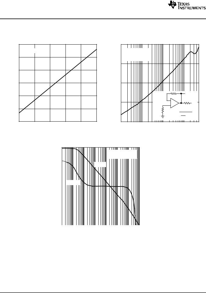
THS4031
THS4032
SLOS224G –JULY 1999 –REVISED MARCH 2010 |
www.ti.com |
||
|
"THS4031M" |
|
|
VIC− Common-Mode Input − ± V
TYPICAL CHARACTERISTICS (continued)
COMMON-MODE INPUT VOLTAGE |
CLOSED-LOOP OUTPUT IMPEDANCE |
vs |
vs |
SUPPLY VOLTAGE |
FREQUENCY |
15 |
|
|
|
|
|
100 |
|
|
|
|
|
TA = 25°C |
|
|
|
Gain = 1 |
|
|
|
|
|
|
|
|
|
|
Ω |
RF = 1 kW |
|
|
|
|
13 |
|
|
|
|
|
|
|
|
|
|
|
|
|
|
− |
PI = + 3 dBm |
|
|
|
||
|
|
|
|
|
Impedance |
10 |
|
|
|
|
|
|
|
|
|
|
|
|
|
|
|
11 |
|
|
|
|
|
|
|
|
|
|
9 |
|
|
|
|
Output |
1 |
|
|
|
|
|
|
|
|
|
|
|
|
|
||
7 |
|
|
|
|
Closed-Loop |
|
|
|
VO |
|
|
|
|
|
|
|
1 kΩ |
|
|||
|
|
|
|
|
|
|
|
|||
|
|
|
|
|
|
|
|
THS403x |
|
|
|
|
|
|
|
|
0.1 |
|
− |
1 kΩ |
VI |
|
|
|
|
|
|
|
+ |
|
||
5 |
|
|
|
|
− |
|
|
50 Ω |
1000 |
|
|
|
|
|
|
O |
|
|
|
||
3 |
|
|
|
|
Z |
0.01 |
|
|
Zo = ( VVOI − 1 ) |
|
|
|
|
|
|
|
10 M |
|
|
||
5 |
7 |
9 |
11 |
13 |
15 |
100 k |
1 M |
100 M |
500 M |
|
|
|
± VCC − Supply V oltage − ± V |
|
|
|
f − Frequency − Hz |
|
|
||
|
|
Figure 14. |
|
|
|
|
|
Figure 15. |
|
|
|
|
100 |
|
OPEN-LOOP GAIN AND PHASE RESPONSE |
45° |
|
|
|||
|
|
|
|
|
|
|
|
|||
|
|
VCC = ± 15 V |
|
|
|
|
RL = 150 Ω |
|
|
|
80 |
|
0° |
|
|
|
|
||
|
|
Gain |
|
|
GainLoop-Open− dB |
60 |
|
−45 ° |
ResponsePhase |
|
||||
|
Phase |
|||
|
40 |
|
−90 ° |
|
|
|
|
||
|
20 |
|
−135 ° |
|
|
|
|
||
|
0 |
|
−180 ° |
|
|
|
|
||
|
−20 |
|
−225 ° |
|
|
|
|
||
100 1 k 10 k 100 k 1 M 10 M 100 M 1 G f − Frequency − Hz
Figure 16.
12 |
Submit Documentation Feedback |
Copyright © 1999–2010, Texas Instruments Incorporated |
Product Folder Link(s): THS4031 THS4032

|
|
|
THS4031 |
|
|
|
THS4032 |
www.ti.com |
SLOS224G –JULY 1999 –REVISED MARCH 2010 |
||
|
"THS4031M" |
|
|
|
|
TYPICAL CHARACTERISTICS (continued) |
|
|
POWER-SUPPLY REJECTION RATIO |
COMMON-MODE REJECTION RATIO |
|
|
vs |
vs |
|
|
FREQUENCY |
FREQUENCY |
|
|
120 |
|
|
|
|
|
|
|
120 |
|
|
THS4032 − V CC+ |
|
|
|
− dB |
|
||
dB |
100 |
|
|
|
|
|
|
100 |
|
Power-Supply Rejection Ratio − |
|
|
|
|
|
|
Common-Mode Rejection Ratio |
||
|
THS4031 − V CC− |
THS4031 − V CC+ |
|
||||||
80 |
|
|
|
80 |
|||||
|
|
|
|
|
|
||||
|
|
|
|
|
|
|
|||
60 |
|
THS4032 − V CC− |
|
|
60 |
||||
|
|
|
|
|
|||||
40 |
|
|
|
|
|
|
40 |
||
|
|
|
|
|
|
|
|
||
− |
20 |
|
|
|
|
|
|
− |
20 |
PSRR |
|
|
|
|
|
|
CMRR |
||
VCC = ± 15 V and ± 5 V |
|
|
|
|
|||||
|
|
|
|
|
|
|
|
||
|
0 |
|
|
|
|
|
|
|
0 |
|
10 |
100 |
1 k |
10 k |
100 k |
1 M |
10 M |
100 M |
|
|
|
|
|
f − Frequency − Hz |
|
|
|
|
|
|
VCC = ± 5 V |
|
|
|
|
|
|
VCC = ± 15 V |
|
|
|
|
|
|
|
1 kΩ |
1 kΩ |
|
|
|
|
|
|
|
|
|
|
|
VI |
|
_ |
VO |
|
|
|
|
+ |
|
|
||
|
|
1 kΩ |
1 kΩ |
RL |
|
|
|
|
|
|
150 Ω |
|
|
10 |
100 |
1 k |
10 k |
100 k |
1 M |
10 M 100 M |
|
|
f − Frequency − Hz |
|
|
||
Figure 17. |
Figure 18. |
THS4032
CROSSTALK vs FREQUENCY
|
0 |
|
|
|
|
|
|
|
VCC = ± 15 V |
|
|
|
|
|
−10 PI = 0 dBm |
|
|
|
||
|
|
See Figure 3 |
|
|
|
|
|
−20 |
|
|
|
|
|
− dB |
−30 |
|
|
|
|
|
−40 |
|
|
|
|
|
|
Crosstalk |
|
|
|
|
|
|
|
Input = CH 2 |
|
|
|
||
−50 |
Output = CH 1 |
|
|
|
||
−60 |
|
|
|
|
|
|
|
|
|
|
|
|
|
|
−70 |
|
|
Input = CH 1 |
|
|
|
|
|
|
Output = CH 2 |
|
|
|
−80 |
|
|
|
|
|
|
−90 |
|
|
|
100 M |
500 M |
|
100 k |
1 M |
10 M |
|||
|
|
|
|
f − Frequency − Hz |
|
|
|
|
|
|
Figure 19. |
|
|
Copyright © 1999–2010, Texas Instruments Incorporated |
Submit Documentation Feedback |
13 |
Product Folder Link(s): THS4031 THS4032
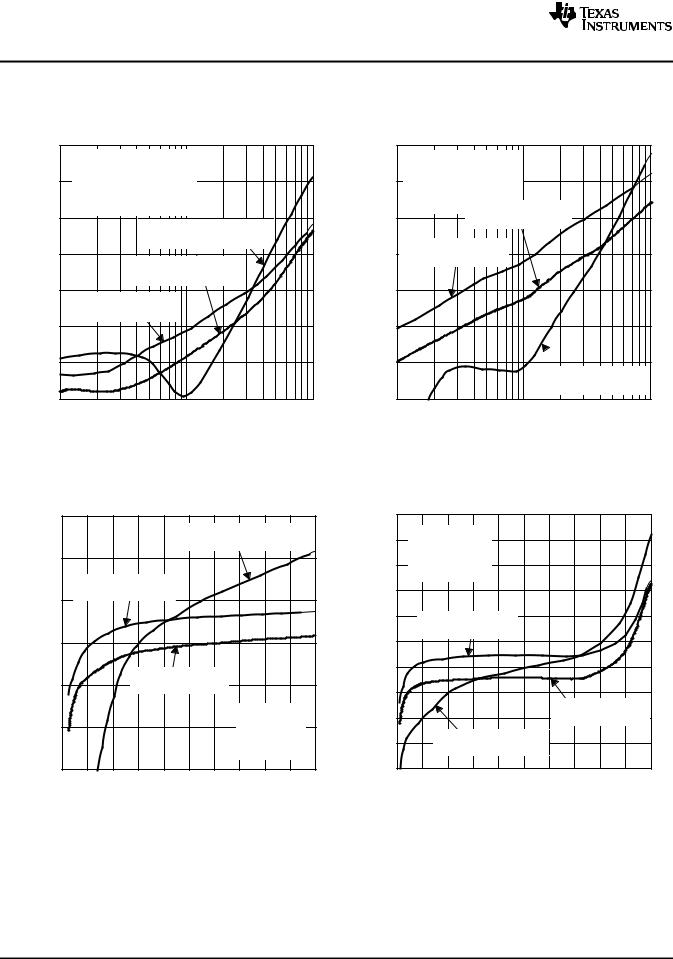
THS4031
THS4032
SLOS224G –JULY 1999 –REVISED MARCH 2010 |
www.ti.com |
||
|
"THS4031M" |
|
|
TYPICAL CHARACTERISTICS (continued)
|
|
HARMONIC DISTORTION |
|
|
|
HARMONIC DISTORTION |
|
||
|
|
|
vs |
|
|
|
|
vs |
|
|
|
|
FREQUENCY |
|
|
|
|
FREQUENCY |
|
|
−40 |
VCC = |
± 15 V and ± 5 V |
|
|
−40 |
VCC = ± 15 V and ± 5 V |
|
|
|
|
|
|
|
|
||||
|
|
Gain = 2 |
|
|
|
Gain = 2 |
|
|
|
|
−50 |
RF = 300 Ω |
|
|
−50 |
RF = 300 Ω |
|
|
|
|
|
RL = 1 kΩ |
|
|
|
RL = 150 Ω |
|
|
|
|
|
V |
= 2 V |
|
|
|
VO(PP) = 2 V |
THS4031 |
|
dBc |
−60 |
O(PP) |
|
|
dBc |
−60 |
|
Second Harmonic |
|
|
THS4031 and THS4032 |
|
|
|
|||||
|
|
|
|
|
|
|
|||
− |
|
|
|
− |
|
|
|
|
|
|
|
Third Harmonics |
|
|
|
|
|
||
Distortion |
|
|
|
Distortion |
|
THS4032 |
|
||
−70 |
|
|
|
−70 |
|
||||
|
THS4031 |
|
Second Harmonic |
|
|||||
|
|
|
|
|
|
|
|||
|
|
Second Harmonic |
|
|
|
|
|
||
−80 |
|
|
|
−80 |
|
|
|
||
Harmonic |
|
THS4032 |
|
Harmonic |
|
|
|
||
|
|
|
|
|
|
|
|||
|
Second Harmonic |
|
|
|
|
|
|||
−90 |
|
|
|
−90 |
|
|
|
||
|
|
|
|
|
|
|
|
||
|
−100 |
|
|
|
|
−100 |
|
THS4031 and THS4032 |
|
|
|
|
|
|
|
|
|
||
|
−110 |
|
|
|
|
−110 |
|
Third Harmonics |
|
|
|
|
10 M |
|
|
|
10 M |
||
|
100 k |
|
1 M |
|
100 k |
1 M |
|||
|
|
|
f − Frequency − Hz |
|
|
|
|
f − Frequency − Hz |
|
|
|
|
Figure 20. |
|
|
|
|
Figure 21. |
|
HARMONIC DISTORTION |
HARMONIC DISTORTION |
vs |
vs |
PEAK-TO-PEAK OUTPUT VOLTAGE |
PEAK-TO-PEAK OUTPUT VOLTAGE |
|
−50 |
|
|
|
|
|
|
|
|
|
|
−10 |
|
|
|
|
|
|
THS4031 and THS4032 |
|
−20 |
||||
|
|
|
|
|
|
Third Harmonics |
|
|
||||
|
−60 |
|
|
|
|
|
|
|
|
|
|
−30 |
|
|
|
|
|
|
|
|
|
|
|
|
|
− dBc |
|
|
|
THS4032 |
|
|
|
|
|
− dBc |
−40 |
|
−70 |
Second Harmonic |
|
|
|
|
|
||||||
|
|
|
|
|
|
|
|
|
|
|||
Distortion |
|
|
|
|
|
|
|
|
|
|
Distortion |
−50 |
−80 |
|
|
|
|
|
|
|
|
|
−60 |
||
|
|
|
|
|
|
|
|
|
|
|||
|
|
|
|
|
|
|
|
|
|
|
||
Harmonic |
|
|
|
THS4031 |
|
|
|
|
|
Harmonic |
−70 |
|
|
|
|
|
|
|
|
|
|
||||
−90 |
|
|
Second Harmonic |
|
|
|
−80 |
|||||
|
|
|
|
|
|
|
|
|
|
|||
|
|
|
|
|
|
|
VCC = ± 15 V |
|
||||
|
|
|
|
|
|
|
|
|
−90 |
|||
|
−100 |
|
|
|
|
|
|
Gain = 5 |
|
|
||
|
|
|
|
|
|
|
RF = 300 Ω |
|
|
|||
|
|
|
|
|
|
|
|
|
|
|||
|
|
|
|
|
|
|
|
RL = 1 kΩ |
|
−100 |
||
|
−110 |
|
|
|
|
|
|
f = 1 MHz |
|
|
−110 |
|
|
|
|
|
|
|
|
14 |
16 |
18 |
20 |
||
|
0 |
2 |
4 |
6 |
8 |
10 |
12 |
|
||||
|
|
VO(PP) − Peak-to-Peak Output V oltage − V |
|
|
||||||||
|
VCC = ± 15 V |
|
|
|
|
|
|
|
|
|
|
Gain = 5 |
|
|
|
|
|
|
|
|
|
|
RF = 300 Ω |
|
|
|
|
|
|
|
|
|
|
RL = 150 Ω |
|
|
|
|
|
|
|
|
|
|
f = 1 MHz |
|
|
|
|
|
|
|
|
|
|
|
|
THS4032 |
|
|
|
|
|
|
|
|
|
Second Harmonic |
|
|
|
|
|
|
||
|
|
|
|
|
|
THS4031 |
|
|
||
|
|
|
|
|
|
Second Harmonic |
|
|||
|
|
THS4031 and THS4032 |
|
|
|
|
|
|||
|
|
Third Harmonics |
|
|
|
|
|
|
||
0 |
2 |
4 |
6 |
8 |
10 |
12 |
14 |
16 |
18 |
20 |
|
VO(PP) − Peak-to-Peak Output V oltage − V |
|
||||||||
Figure 22. |
Figure 23. |
14 |
Submit Documentation Feedback |
Copyright © 1999–2010, Texas Instruments Incorporated |
Product Folder Link(s): THS4031 THS4032
 Loading...