


Texas Instruments THS6032IGQER, THS6032IDWPR, THS6032IDWP, THS6032CGQER, THS6032EVM Datasheet
...
|
|
|
|
|
THS6032 |
|
|
LOW-POWER ADSL CENTRAL-OFFICE LINE DRIVER |
|||||
|
|
|
SLOS233C ± APRIL1999 ± REVISED MARCH 2000 |
|||
D Low Power ADSL Line Driver Ideal for |
THERMALLY ENHANCED SOIC (DWP) |
|||||
|
Central Office |
|
PowerPAD PACKAGE |
|
||
|
|
(TOP VIEW) |
|
|
||
|
± 1.35-W Total Power Dissipation for |
|
|
|
||
|
|
|
|
|
||
|
Full-Rate ADSL Into a 25-Ω Load |
PAD² |
1 |
20 |
PAD² |
|
D |
Low-Impedance Shutdown Mode |
VCCH± |
2 |
19 |
VCCH+ |
|
|
± Allows Reception of Incoming Signal |
1OUT |
3 |
18 |
2OUT |
|
|
During Standby |
VCCL± |
4 |
17 |
VCCL+ |
|
D Two Modes of Operation |
1IN± |
5 |
16 |
2IN± |
||
1IN+ |
6 |
15 |
2IN+ |
|||
|
± Class-G Mode: 4 Power Supplies, 1.35 W |
|||||
|
NC |
7 |
14 |
NC |
||
|
Power Dissipation |
|||||
|
SHDN1 |
8 |
13 |
NC |
||
|
± Class-AB Mode: 2 Power Supplies, 2 W |
|||||
|
SHDN2 |
9 |
12 |
DGND |
||
|
Power Dissipation |
|||||
|
PAD² |
10 |
11 |
PAD² |
||
|
Low Distortion |
|||||
D |
NC ± Not Connected |
|
|
|||
|
± THD = ±62 dBc at f = 1 MHz, |
|
|
|||
|
VO(PP) = 20 V, 25-Ω Load |
|
(SIDE VIEW) |
|
|
|
|
|
|
|
|
||
|
± THD = ±69 dBc at f = 1 MHz, |
|
|
|
|
|
|
VO(PP) = 2 V, 25-Ω Load |
|
|
|
|
|
D 400-mA Minimum Output Current Into a |
|
|
|
|
||
|
25-Ω Load |
Cross section view showing PowerPAD |
||||
D |
High Speed |
² This terminal is internally connected to the thermal pad. |
||||
|
|
|
|
|||
|
± 65-MHz Bandwidth (±3dB) , 25-Ω Load |
MicroStar Junior (GQE) PACKAGE |
||||
|
± 100-MHz Bandwidth (±3dB) , 100-Ω Load |
|
(TOP VIEW) |
|
|
|
|
± 1200 V/µs Slew Rate |
|
|
|
|
|
D Thermal Shutdown and Short Circuit |
|
|
|
|
||
|
Protection |
|
|
|
|
|
D |
Evaluation Module Available |
|
|
|
|
|
description
The THS6032 is a low-power line driver ideal for asymmetrical digital subscriber line (ADSL) applications. This device contains two high-current, high-speed current-feedback drivers, which can be configured differentially for driving ADSL signals at the central office. The THS6032 features a unique class-G architecture to lower power consumption to 1.35 W. The THS6032 can also be operated in a traditional class-AB mode to reduce the number of power supplies to two.
HIGH-SPEED xDSL LINE DRIVER/RECEIVER FAMILY
DEVICE |
DRIVER |
RECEIVER |
5 V |
± 5 V |
±15 V |
DESCRIPTION |
THS6002 |
• |
• |
|
• |
• |
500-mA differential line driver and receiver |
THS6012 |
• |
|
|
• |
• |
500-mA differential line driver |
THS6022 |
• |
|
|
• |
• |
250-mA differential line driver |
THS6032 |
• |
|
|
• |
• |
500-mA low-power ADSL central-office line driver |
THS6062 |
|
• |
• |
• |
• |
Low-noise ADSL receiver |
THS6072 |
|
• |
|
• |
• |
Low-power ADSL receiver |
THS7002 |
|
• |
|
• |
• |
Low-noise programmable-gain ADSL receiver |
CAUTION: The THS6032 provides ESD protection circuitry. However, permanent damage can still occur if this device is subjected to high-energy electrostatic discharges. Proper ESD precautions are recommended to avoid any performance degradation or loss of functionality.
Please be aware that an important notice concerning availability, standard warranty, and use in critical applications of Texas Instruments semiconductor products and disclaimers thereto appears at the end of this data sheet.
PowerPAD and MicroStar Junior are trademarks of Texas Instruments.
PRODUCTION DATA information is current as of publication date. Products conform to specifications per the terms of Texas Instruments standard warranty. Production processing does not necessarily include testing of all parameters.
Copyright 2000, Texas Instruments Incorporated
POST OFFICE BOX 655303 •DALLAS, TEXAS 75265 |
1 |
THS6032
LOW-POWER ADSL CENTRAL-OFFICE LINE DRIVER
SLOS233C ± APRIL1999 ± REVISED MARCH 2000
description
The class-G architecture supplies current to the load from four supplies. For low output voltages (typically
±2.5 < VO < +2.5), some of the output current is supplied from the +VCC(L) and ±VCC(L) supplies (typically ± 5 V). For large output voltages (typically VO < ±2.5 and VO > +2.5), the output current is supplied from +VCC(H) and ±VCC(H) (typically ± 15 V). This current sharing between VCC(L) and VCC(H) minimizes power dissipation within the THS6032 output stages for high crest factor ADSL signals.
The THS6032 features a low-impedance shutdown mode, which allows the central office to receive incoming calls even after the device has been shut down. The THS6032 is available packaged in the patented PowerPAD package. This package provides outstanding thermal characteristics in a small-footprint surface-mount package, which is fully compatible with automated surface-mount assembly procedures. It is also available in the new MicoStar Junior BGA package. This package is only 25 mm2 in area, allowing for high density PCB designs.
Shutdown (SHDN1 and SHDN2) allows for powering down the internal circuitry for power conservation or for multiplexing. Separate shutdown controls are available for each channel on the THS6032. The control levels are TTL compatible. When turned off, each driver output is placed in a low impedance state which is determined by the voltage at DGND. This virtual ground at the outputs allows proper termination of a transmission line.
AVAILABLE OPTIONS
|
PACKAGED DEVICES |
PACKAGED DEVICES |
|
|
TA |
PowerPAD PLASTIC SMALL OUTLINE |
MicroStar Junior (BGA) |
EVALUATION MODULES |
|
|
(DWP) |
(GQE) |
|
|
|
|
|
|
|
0°C to 70°C |
THS6032CDWP |
THS6032CGQE |
THS6032EVM |
|
THS6032GQE EVM³ |
||||
|
|
|
||
± 40°C to 85°C |
THS6032IDWP |
THS6032IGQE |
Ð |
² The THS6032 is available taped and reeled. Add an R suffix to the device type (i.e.,THS6032CDWPR) ³ Uses the THS6032CGQE packaging option.
Terminal Functions
TERMINAL
|
NAME |
DWP PACKAGE |
GQE PACKAGE |
|
|
|
TERMINAL NO. |
TERMINAL NO. |
|
|
|
|
|
|
|
1OUT |
3 |
B1 |
|
|
|
|
|
|
|
1IN± |
5 |
F1 |
|
|
|
|
|
|
|
1IN+ |
6 |
H1 |
|
|
|
|
|
|
|
2OUT |
18 |
B9 |
|
|
|
|
|
|
|
2IN± |
16 |
F9 |
|
|
|
|
|
|
|
2IN+ |
15 |
H9 |
|
|
|
|
|
|
|
VCCH± |
2 |
A3 |
|
|
VCCH+ |
19 |
A7 |
|
|
VCCL± |
4 |
D1 |
|
|
VCCL+ |
17 |
D9 |
|
|
SHDN1 |
8 |
J2 |
|
|
|
|
|
|
|
SHDN2 |
9 |
J4 |
|
|
|
|
|
|
|
DGND |
12 |
J7 |
|
|
|
|
|
|
|
PAD |
1, 10, 11, 20 |
N/A |
|
|
|
|
|
|
|
NC |
7, 13, 14 |
N/A |
|
|
|
|
|
|
|
|
|
|
|
2 |
POST OFFICE BOX 655303 •DALLAS, TEXAS 75265 |
THS6032
LOW-POWER ADSL CENTRAL-OFFICE LINE DRIVER
SLOS233C ± APRIL1999 ± REVISED MARCH 2000
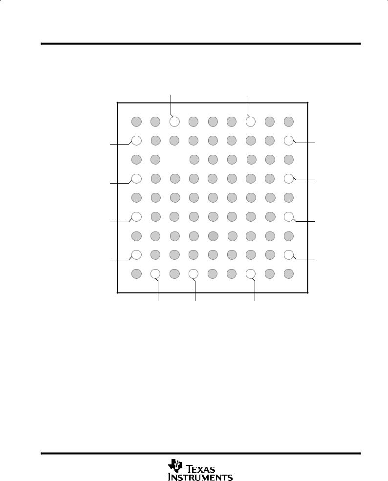
pin assignments
MicroStar Junior (GQE) PACKAGE
(TOP VIEW)
|
|
|
CCH± |
|
|
|
CCH+ |
|
|
|
|
|
V |
|
|
|
V |
|
|
|
1 |
2 |
3 |
4 |
5 |
6 |
7 |
8 |
9 |
A |
NC |
NC |
|
NC |
NC |
NC |
|
NC |
NC |
B |
|
NC |
NC |
NC |
NC |
NC |
NC |
NC |
2OUT |
1OUT |
|
|
|
|
|
|
|
|
|
C |
NC |
NC |
|
NC |
NC |
NC |
NC |
NC |
NC |
D |
|
NC |
NC |
NC |
NC |
NC |
NC |
NC |
VCCL+ |
VCCL± |
|
|
|
|
|
|
|
|
|
E |
NC |
NC |
NC |
NC |
NC |
NC |
NC |
NC |
NC |
F |
|
NC |
NC |
NC |
NC |
NC |
NC |
NC |
|
1IN± |
|
|
|
|
|
|
|
|
2IN± |
G |
NC |
NC |
NC |
NC |
NC |
NC |
NC |
NC |
NC |
H |
|
NC |
NC |
NC |
NC |
NC |
NC |
NC |
2IN+ |
1IN+ |
|
|
|
|
|
|
|
|
|
J |
NC |
|
NC |
|
NC |
NC |
|
NC |
NC |
|
|
SHDN1 |
|
SHDN2 |
|
|
DGND |
|
|
NOTE: Shaded terminals are used for thermal connection to the ground plane.
POST OFFICE BOX 655303 •DALLAS, TEXAS 75265 |
3 |
THS6032
LOW-POWER ADSL CENTRAL-OFFICE LINE DRIVER
SLOS233C ± APRIL1999 ± REVISED MARCH 2000
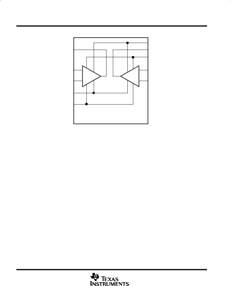
functional block diagram (SOIC package)
|
|
19 |
VCCH+ |
|
|
|
|
||
1OUT |
3 |
18 |
2OUT |
|
|
|
|||
|
|
17 |
VCCL+ |
|
|
|
|
||
1IN± |
5 |
16 |
2IN± |
|
± |
± |
|||
1IN+ |
6 |
15 |
2IN+ |
|
+ |
+ |
|||
VCCH± |
2 |
|
|
|
VCCL± |
4 |
|
|
|
|
|
|
||
SHDN1 |
8 |
12 |
DGND |
|
SHDN2 |
9 |
|||
|
|
NOTE A: Terminals 1, 10, 11, and 20 are internally connected to the thermal pad.
absolute maximum ratings over operating free-air temperature (unless otherwise noted)²
Supply voltage, VCC(L) and VCC(H) (see Note 1) . . . . . . . . . . . . . . . . . . . . . . . . . . |
. . . . . . . . . . . . . . . . . . . . . 33 V |
Input voltage, VI . . . . . . . . . . . . . . . . . . . . . . . . . . . . . . . . . . . . . . . . . . . . . . . . . . . . . . |
. . . . . . . . . . . . . . . . . . . ±VCCH |
Output current, IO (see Note 2) . . . . . . . . . . . . . . . . . . . . . . . . . . . . . . . . . . . . . . . . . |
. . . . . . . . . . . . . . . . . . 800 mA |
Differential input voltage, VID . . . . . . . . . . . . . . . . . . . . . . . . . . . . . . . . . . . . . . . . . . . |
. . . . . . . . . . . . . . . . . . . . . ± 4 V |
Total power dissipation at (or below) 25°C free-air temperature |
|
(see Note 2) . . . . . . . . . . . . . . . . . . . . . . . . . . . . . . . . . . . . . . . . . . . . . . . . . . . . . . |
See Dissipation Rating Table |
Maximum junction temperature, TJ . . . . . . . . . . . . . . . . . . . . . . . . . . . . . . . . . . . . . . |
. . . . . . . . . . . . . . . . . . . 150°C |
Operating free-air temperature, TA, C-suffix . . . . . . . . . . . . . . . . . . . . . . . . . . . . . . |
. . . . . . . . . . . . . . 0°C to 70°C |
I-suffix . . . . . . . . . . . . . . . . . . . . . . . . . . . . . . |
. . . . . . . . . . . . ±40°C to 85°C |
Storage temperature, Tstg . . . . . . . . . . . . . . . . . . . . . . . . . . . . . . . . . . . . . . . . . . . . . . |
. . . . . . . . . . . ±65°C to 125°C |
Lead temperature 1,6 mm (1/16 in) from case for 10 seconds . . . . . . . . . . . . . . . |
. . . . . . . . . . . . . . . . . . . 300°C |
²Stresses beyond those listed under ªabsolute maximum ratingsº may cause permanent damage to the device. These are stress ratings only, and functional operation of the device at these or any other conditions beyond those indicated under ªrecommended operating conditionsº is not implied. Exposure to absolute-maximum-rated conditions for extended periods may affect device reliability.
NOTES: 1. VCC(L) must always be less than or equal to VCC(H)
2.The THS6032 incorporates a PowerPAD on the underside of the chip. This acts as a heatsink and must be connected to a thermally dissipative plane for proper power dissipation. Failure to do so may result in exceeding the maximum junction temperature which could permanently damage the device. See the Thermal Information section for more information about utilizing the PowerPAD thermally enhanced packages.
DISSIPATION RATING TABLE³
PACKAGE |
θJA |
θJC |
TA = 25°C |
|
(°C/W) |
(°C/W) |
POWER RATING |
||
|
||||
|
|
|
|
|
DWP |
21.5 |
0.37 |
5.8 W |
|
|
|
|
|
|
GQE |
37.8 |
4.56 |
3.3 W |
³This data was taken using 2 oz. trace and copper pad that is soldered directly to a JEDEC standard 4 layer 3 in × 3 in PCB.
4 |
POST OFFICE BOX 655303 •DALLAS, TEXAS 75265 |

THS6032
LOW-POWER ADSL CENTRAL-OFFICE LINE DRIVER
SLOS233C ± APRIL1999 ± REVISED MARCH 2000
recommended operating conditions
|
|
MIN |
NOM |
MAX |
UNIT |
|
|
|
|
|
|
|
VCC(L) ± Class G mode |
± 3 |
± 5 |
± VCCH |
V |
Supply voltage |
VCC(L) ± Class AB mode |
0 |
0 |
0 |
V |
|
VCC(H) |
± 5 |
± 15 |
± 16 |
V |
Operating free-air temperatures, TA |
C-suffix |
0 |
|
70 |
°C |
|
|
|
|
||
I-suffix |
± 40 |
|
85 |
||
|
|
|
|||
|
|
|
|
|
|
electrical characteristics, VCC(L) = ±5 V, VCC(H) = ±15 V, RL = 25 Ω,TA = 25 °C (unless otherwise noted) dynamic performance
|
PARAMETER |
TEST CONDITIONS |
MIN TYP |
MAX |
UNIT |
|
|
|
|
|
|
|
|
|
|
Gain = 1, RF = 1.3 kΩ |
RL = 25 Ω |
65 |
|
MHz |
|
Small signal bandwidth (±3 dB) |
RL = 100 Ω |
100 |
|
||
|
|
|
|
|||
|
Gain = 2, RF = 1.1 kΩ |
RL = 25 Ω |
60 |
|
MHz |
|
|
|
|
||||
BW |
|
RL = 100 Ω |
70 |
|
||
|
|
|
|
|||
|
Bandwidth for 0.1 dB flatness |
Gain = 1 |
|
30 |
|
MHz |
|
|
|
|
|
||
|
Gain = 2 |
|
25 |
|
||
|
|
|
|
|
||
|
|
|
|
|
|
|
|
Full power bandwidth² |
VOPP = 20 V |
|
19 |
|
MHz |
SR |
Slew rate³ |
Gain = 5, |
VO(PP) = 20 V |
1200 |
|
V/µs |
ts |
Settling time to 0.1% |
Gain = 1, RL = 25 Ω, |
5 V Step |
120 |
|
ns |
² Full power bandwidth = slew rate/2π VPEAK
³ Slew rate is defined from the 25% to the 75% output levels.
noise/distortion performance
|
PARAMETER |
|
TEST CONDITIONS |
MIN |
TYP |
MAX |
UNIT |
|||
|
|
|
|
|
|
|
|
|
|
|
THD |
Total harmonic distortion |
VO = 20 V(pp), Gain = 5, |
f = 1 MHz |
|
± 62 |
|
dBc |
|||
VO = 2 V(pp), Gain = 2, |
f = 1 MHz |
|
± 69 |
|
||||||
|
|
|
|
|
|
|
||||
Vn |
Input voltage noise |
f = 10 kHz |
|
|
|
2.4 |
|
nV/√ |
|
|
|
|
|
|
Hz |
|
|||||
|
|
|
|
In+ |
|
11 |
|
|
|
|
In |
Input current noise |
f = 10 kHz |
|
|
|
nV/√ Hz |
||||
|
In± |
|
15 |
|
||||||
|
|
|
|
|
|
|
|
|
||
|
Differential gain error |
Gain = 2, |
NTSC |
RL = 150 Ω |
|
0.016% |
|
|
|
|
|
RL = 25 Ω |
|
0.020% |
|
|
|
|
|||
|
|
|
|
|
|
|
|
|
||
|
Differential phase error |
Gain = 2, |
NTSC |
RL = 150 Ω |
|
0.04° |
|
|
|
|
|
RL = 25 Ω |
|
0.30° |
|
|
|
|
|||
|
|
|
|
|
|
|
|
|
||
|
Crosstalk |
f = 1 MHz, Gain = 2, |
RF = 1.1 kΩ |
|
± 62 |
|
dB |
|||
POST OFFICE BOX 655303 •DALLAS, TEXAS 75265 |
5 |

THS6032
LOW-POWER ADSL CENTRAL-OFFICE LINE DRIVER
SLOS233C ± APRIL1999 ± REVISED MARCH 2000
electrical characteristics, VCC(L) = ±5 V, VCC(H) = ±15 V, RL = 25 Ω,TA = 25 °C (unless otherwise noted)
(continued)
dc performance
|
PARAMETER |
TEST CONDITIONS |
MIN TYP |
MAX |
UNIT |
|
|
|
|
|
|
|
|
Z(t) |
Open loop transimpedance |
RL = 1 kΩ |
2 |
|
MΩ |
|
VIO |
Input offset voltage |
TA = 25°C |
1.5 |
5 |
mV |
|
TA = full range |
|
7 |
||||
|
|
|
|
|||
|
Offset voltage drift |
|
|
10 |
µV/°C |
|
|
|
|
|
|
|
|
|
Differential offset voltage |
TA = 25°C |
0.5 |
3 |
mV |
|
|
TA = full range |
|
6 |
|||
|
|
|
|
|||
|
Negative input bias current |
TA = 25°C |
1.5 |
9 |
|
|
IIB |
TA = full range |
|
12 |
µA |
||
|
|
|||||
Positive input bias current |
TA = 25°C |
1.5 |
9 |
|||
|
|
|||||
|
TA = full range |
|
12 |
|
||
|
|
|
|
input characteristics
|
PARAMETER |
TEST CONDITIONS |
MIN |
TYP |
MAX |
UNIT |
|
|
|
|
|
|
|
VICR |
Input common-mode voltage range |
|
± 13.2 |
± 13.4 |
|
V |
CMRR |
Common-mode rejection ratio |
TA = full range |
64 |
72 |
|
dB |
ri |
Input resistance |
Inverting terminal |
|
15 |
|
Ω |
Non inverting terminal |
|
400 |
|
kΩ |
||
|
|
|
|
|||
|
|
|
|
|
|
|
|
Differential input capacitance |
|
|
1.4 |
|
pF |
|
|
|
|
|
|
|
output characteristics
|
PARAMETER |
|
TEST CONDITIONS |
MIN |
TYP |
MAX |
UNIT |
|||
|
|
|
|
|
|
|
|
|
||
VO |
Output voltage |
Single-ended |
RL = 25 |
Ω |
± 10.5 |
± 11 |
|
V |
||
Differential |
RL = 50 |
Ω |
± 21 |
± 22 |
|
|||||
|
|
|
|
|||||||
I |
Output current² |
|
R |
L |
= 25 |
Ω |
400 |
440 |
|
mA |
O |
|
|
|
|
|
|
|
|
|
|
I |
Short-circuit current² |
|
|
|
|
|
800 |
|
mA |
|
SC |
|
|
|
|
|
|
|
|
|
|
²A heat sink is required to keep junction temperature below absolute maximum when an output is heavily loaded or shorted. See ªabsolute maximum ratings.º
power supply
|
PARAMETER |
TEST CONDITIONS |
MIN |
TYP |
MAX |
UNIT |
|
|
|
|
|
|
|
|
|
VCC |
Operating range |
VCCL |
|
0 |
± 5 ±VCCH |
V |
|
VCCH |
|
± 5 |
± 15 |
± 16.5 |
|||
|
|
|
|
||||
|
|
VCCL |
TA = 25°C |
|
4.3 |
5.8 |
mA |
ICC |
Quiescent current (per amplifier) |
TA = full range |
|
|
6.2 |
||
|
|
|
|
||||
VCCH |
TA = 25°C |
|
4 |
5 |
mA |
||
|
|
|
|||||
|
|
TA = full range |
|
|
5.5 |
||
|
|
|
|
|
|
||
|
|
VCCL |
TA = 25°C |
90 |
100 |
|
dB |
|
|
|
|
|
|
||
PSRR |
Power supply rejection ratio |
TA = full range |
80 |
|
|
||
|
|
|
|
||||
VCCH |
TA = 25°C |
69 |
80 |
|
dB |
||
|
|
|
|||||
|
|
|
|
|
|
||
|
|
TA = full range |
66 |
|
|
||
6 |
POST OFFICE BOX 655303 •DALLAS, TEXAS 75265 |

THS6032
LOW-POWER ADSL CENTRAL-OFFICE LINE DRIVER
SLOS233C ± APRIL1999 ± REVISED MARCH 2000
electrical characteristics, VCC(L) = ±5 V, VCC(H) = ±15 V, RL = 25 Ω,TA = 25 °C (unless otherwise noted)
(continued)
shutdown characteristics
|
PARAMETER |
TEST CONDITIONS |
MIN TYP |
MAX |
UNIT |
|||
|
|
|
|
|
|
|||
VIL |
Shutdown voltage for power up |
Relative to DGND terminal |
|
0.8 |
V |
|||
VIH |
Shutdown voltage for power down |
Relative to DGND terminal |
2 |
|
V |
|||
IIH |
Shutdown input current-high |
V(SHDN) = 5 V |
|
|
200 |
300 |
µA |
|
IIL |
Shutdown input current-low |
V(SHDN) = 0.5 |
V |
|
20 |
40 |
µA |
|
Zo |
Output impedance (while in shutdown state) |
V(SHDN) = 2.5 |
V, |
f = 1 MHz |
0.5 |
|
Ω |
|
ICCL |
Supply current (per amplifier) (while in shutdown state) |
V(SHDN) = 2.5 |
V, |
VO = 0 V |
0.05 |
0.2 |
mA |
|
ICCH |
2.4 |
3 |
||||||
|
|
|
|
|
||||
t |
Disable time² |
|
|
|
1.1 |
|
µS |
|
dis |
|
|
|
|
|
|
|
|
t |
Enable time² |
|
|
|
1.5 |
|
µS |
|
en |
|
|
|
|
|
|
|
|
²Disable/enable time begins when the logic signal is applied to the shutdown terminal and ends when the supply current has reached half of its final value.
POST OFFICE BOX 655303 •DALLAS, TEXAS 75265 |
7 |

THS6032
LOW-POWER ADSL CENTRAL-OFFICE LINE DRIVER
SLOS233C ± APRIL1999 ± REVISED MARCH 2000
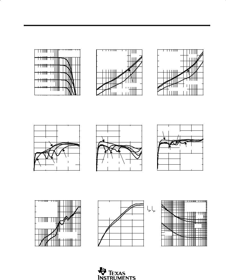
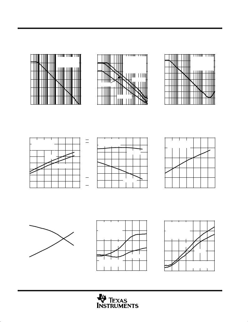
TYPICAL CHARACTERISTICS
OUTPUT AMPLITUDE |
OUTPUT AMPLITUDE |
|
|
|
vs |
|
|
|
|
vs |
|
|
|
|
|
FREQUENCY |
|
|
|
FREQUENCY |
|
|
|||
|
2 |
|
|
|
|
|
0.4 |
|
|
|
|
|
1 |
RF = 1 kΩ |
RF = 1.3 kΩ |
|
|
0.3 |
VCC(H) = ± 15 V |
|
|
|
|
|
|
|
VCC(L) = ± 5 V |
|
|
|
|||||
|
|
|
|
|
|
|
|||||
|
0 |
|
|
|
|
|
0.2 |
Gain = +1 |
|
|
dB± |
dB± |
|
|
|
|
dB± |
|
|
|
|||
±1 |
|
|
|
|
VO = 0.2 VRMS |
|
|
||||
|
|
|
|
|
|
|
|
RL = 25 Ω |
|
|
|
Amplitude |
|
RF = 1.5 kΩ |
|
|
Amplitude |
0.1 |
|
|
|
Amplitude |
|
±2 |
|
|
|
RF = 1 kΩ |
|
|
|||||
|
|
|
|
|
|
|
|
||||
|
|
|
|
|
|
±0.0 |
|
|
|
||
|
±3 |
|
|
|
|
|
|
|
|
|
|
|
|
|
|
|
|
|
|
|
|
|
|
Output |
±4 |
VCC(L) = ± 5 V |
|
|
|
Output |
±0.1 |
|
|
|
Output |
|
|
|
±0.2 |
|
|
|
|||||
|
|
VCC(H) = ± 15 V |
|
|
|
|
|
RF = 1.3 kΩ |
|
|
|
|
±5 |
Gain = +1 |
|
|
|
|
|
|
|
|
|
|
|
|
|
|
|
|
|
|
|
|
|
|
±6 |
RL = 25 Ω |
|
|
|
|
±0.3 |
RF = 1.5 kΩ |
|
|
|
|
|
|
|
|
|
|
|
|
|||
|
±7 |
VO = 0.2 VRMS |
|
|
|
|
±0.4 |
|
|
|
|
|
|
|
|
|
|
|
|
|
|
||
|
100 k |
1 M |
10 M |
100 M |
500 M |
|
100 k |
1 M |
10 M |
100 M |
500 M |
|
|
f ± Frequency ± Hz |
|
|
|
f ± Frequency ± Hz |
|
|
|||
|
OUTPUT AMPLITUDE |
|
||
|
|
vs |
|
|
|
FREQUENCY |
|
||
8 |
|
|
|
|
7 |
RF = 820 Ω |
|
RF = 1.1 kΩ |
|
6 |
|
|
|
|
5 |
|
|
|
|
4 |
RF = 1.3 kΩ |
|
|
|
|
|
|
||
3 |
|
|
|
|
2 |
VCC(H) = ± 15 V |
|
|
|
|
|
|
|
|
1 |
VCC(L) = ± 5 V |
|
|
|
Gain = +2 |
|
|
|
|
|
|
|
|
|
0 |
RL = 25 Ω |
|
|
|
±1 |
VO = 0.4 VRMS |
|
|
|
|
|
|
|
|
100 k |
1 M |
10 M |
100 M |
500 M |
|
f ± Frequency ± Hz |
|
||
Figure 1 |
Figure 2 |
|
|
OUTPUT AMPLITUDE |
|
|
|
OUTPUT AMPLITUDE |
|
||||
|
|
|
vs |
|
|
|
|
vs |
|
|
|
|
|
FREQUENCY |
|
|
|
|
FREQUENCY |
|
|
||
|
6.4 |
|
|
|
|
|
16 |
|
|
|
|
|
|
VCC(H) = ± 15 V |
|
|
|
|
15 |
RF = 330 Ω |
|
|
|
|
6.3 |
VCC(L) = ± 5 V |
|
|
|
|
|
|
|
|
|
|
|
Gain = +2 |
|
|
|
|
14 |
|
|
|
|
± dB |
6.2 |
RL = 25 Ω |
|
|
|
± dB |
|
|
|
|
|
|
|
|
|
|
|
|
|
||||
6.1 |
VO = 0.4 VRMS |
|
|
|
13 |
RF = 820 Ω |
|
|
|
||
Amplitude |
|
|
|
|
Amplitude |
|
|
|
|
||
|
|
|
|
|
|
|
|
|
|||
6.0 |
RF = 820 Ω |
|
|
|
12 |
RF = 1.5 kΩ |
|
|
|
||
|
|
|
|
|
|
|
|
||||
|
|
|
|
|
|
11 |
|
|
|
||
|
|
|
|
|
|
|
|
|
|
|
|
Output |
5.9 |
RF = 1.1 kΩ |
|
|
Output |
10 |
VCC(L) = ± 5 V |
|
|
|
|
5.8 |
|
|
|
|
|
||||||
|
|
|
|
|
VCC(H) = ± 15 V |
|
|
|
|||
|
|
|
|
|
|
|
9 |
Gain = +5 |
|
|
|
|
|
RF = 1.3 kΩ |
|
|
|
|
|
|
|
|
|
|
5.7 |
|
|
|
|
8 |
RL= 25 Ω |
|
|
|
|
|
5.6 |
|
|
|
|
|
7 |
Vo = 0.2 VRMS |
|
|
|
|
|
|
|
|
|
|
|
|
|
||
|
100 k |
1 M |
10 M |
100 M |
500 M |
|
100k |
1M |
10M |
100M |
500M |
|
|
f ± Frequency ± Hz |
|
|
|
|
f ± Frequency ± Hz |
|
|
||
Output Amplitude ± dB
Figure 3
OUTPUT AMPLITUDE vs
FREQUENCY
22
21 |
|
|
RF = 510 Ω |
|
|
|
|
|
|
20 |
|
|
|
|
19 |
|
|
|
|
18 |
RF = 1 kΩ |
|
|
|
|
|
|
|
|
17 |
|
|
|
|
16 |
VCC(H) = ± 15 V |
|
|
|
15 |
VCC(L) = ± 5 V |
|
|
|
Gain = +10 |
|
|
|
|
14 |
RL= 25 Ω |
|
|
|
Vo = 0.2 VRMS |
|
|
|
|
|
|
|
|
|
13 |
|
|
|
|
100k |
1M |
10M |
100M |
500M |
|
f ± Frequency ± Hz |
|
||
Figure 4 |
Figure 5 |
Figure 6 |
|
|
|
CLASS-AB MODE OUTPUT AMPLITUDE |
OUTPUT AMPLITUDE |
|
vs |
vs |
SMALL AND LARGE SIGNAL |
FREQUENCY |
FREQUENCY |
FREQUENCY RESPONSE |
Class-AB Mode Output Amplitude ± dB
8 |
|
|
|
|
|
8 |
|
|
|
|
|
18 |
|
|
|
VCC(H) = ± 15 V |
|
|
6 |
|
|
|
|
|
|
Gain = +2, RF = 1.1 kΩ |
|
|
dBV± |
12 |
|
|
|
|
|||
|
|
|
|
|
6 |
|
|
|
|
|
|
|
VCC(L) = ± 5 V |
|
||||
|
|
|
|
|
dB±AmplitudeOutput |
|
|
|
|
VoltageOutputNormalized |
VO(PP) = 4 V |
|
||||||
|
G = +2 |
|
|
|
4 |
|
|
|
|
VO(PP) = 0.25 V |
|
|
|
|||||
|
|
|
|
|
|
|
|
|
|
|
|
|
|
|
|
|
||
4 |
RF =1.1 kΩ |
|
|
|
|
|
|
|
|
VO(PP) = 2 V |
|
|
|
|||||
|
|
|
|
|
|
|
|
|
|
|
|
|||||||
|
|
|
|
|
|
2 |
|
|
|
|
|
6 |
|
|
|
|
|
|
2 |
VCC(H) = ± 15 V |
|
|
|
|
|
|
|
|
|
|
|
|
|
|
|
||
|
|
|
|
Gain = +1, RF = 1.3 kΩ |
|
|
|
V |
O(PP) |
= 1 V |
|
|
|
|||||
|
VCC(L) = GND |
|
|
|
0 |
|
|
|
|
|
|
|||||||
|
|
|
|
|
|
|
|
|
0 |
|
|
|
|
|
||||
0 |
|
|
|
|
|
±2 |
|
|
|
|
|
VO(PP) = 0.5 V |
|
|
|
|||
|
G = +1 |
|
|
|
|
|
|
|
|
|
|
|
|
|||||
±2 |
RF =1.3 kΩ |
|
|
|
|
|
|
|
|
|
±6 |
|
|
|
|
|
|
|
|
|
|
±4 VCC(H) = ± 15 V |
|
|
|
|
|
|
|
|
|
|
|
||||
|
|
|
|
|
|
|
|
|
|
|
|
|
|
|
|
|
||
±4 |
RL = 25 Ω |
|
|
|
±6 |
VCC(L) = ± 5 V |
|
|
|
± |
±12 |
|
|
|
|
|
|
|
|
|
|
RL = 100 Ω |
|
|
|
O |
Gain = +1 |
|
|
|
|
||||||
|
VI = 0.2 VRMS |
|
|
|
|
|
|
|
|
|
|
|||||||
|
|
|
|
|
VIN = 0.2 VRMS |
|
|
|
V |
RL = 25 Ω |
RF = 1.3 k Ω |
|
|
|||||
±6 |
|
|
|
|
|
±8 |
|
|
|
|
|
|
||||||
|
|
|
|
|
|
|
|
|
|
±18 |
|
|
|
|
|
|
||
100 k |
1 M |
10 M |
100 M |
500 M |
|
100 k |
1 M |
10 M |
100 M |
500 M |
|
100 k |
1 M |
10 M |
100 M |
500 M |
||
|
|
f ± Frequency ± Hz |
|
|
|
|
f ± Frequency ± Hz |
|
|
|
|
|
f ± Frequency ± Hz |
|
|
|||
|
|
Figure 7 |
|
|
|
|
Figure 8 |
|
|
|
|
|
|
Figure 9 |
|
|
||
8 |
POST OFFICE BOX 655303 •DALLAS, TEXAS 75265 |
THS6032 LOW-POWER ADSL CENTRAL-OFFICE LINE DRIVER
SLOS233C ± APRIL1999 ± REVISED MARCH 2000
TYPICAL CHARACTERISTICS
|
CLASS-G MODE DISTORTION |
SMALL AND LARGE SIGNAL |
vs |
FREQUENCY RESPONSE |
FREQUENCY |
|
24 |
|
|
VCC(H) = ± 15 V |
|
|
±20 |
|
|
|
|
VoltageOutputNormalized± ± dBV |
|
VO(PP) = 8 V |
|
|
|
VCC(H) = ± 15 V |
|
|
|||
18 |
VCC(L) = ± 5 V |
|
DistortionModeG-Class± dBc |
±30 |
VCC(L) = ± 5 V to ± 7.5 V |
THD |
|
||||
|
|
|
|
||||||||
±6 |
|
|
|
|
|
±40 |
Gain = +2 |
|
|
||
VO(PP) = 4 V |
|
|
|
RF = 1.1 kΩ |
|
|
|||||
|
|
|
|
|
|
|
|
||||
|
|
|
|
|
|
|
|
|
|||
|
12 |
|
|
|
|
|
|
±50 |
RL = 25 Ω |
|
|
|
|
|
|
|
|
|
|
VO(PP) = 2 V |
|
|
|
|
|
VO(PP) = 2 V |
|
|
|
|
|
|
|
||
|
6 |
|
|
|
|
±60 |
|
|
|
||
|
|
|
|
|
|
|
|
|
|
||
|
|
VO(PP) = 1 V |
|
|
|
|
±70 |
|
|
|
|
|
0 |
|
|
|
|
|
|
|
|
|
|
|
|
|
|
|
|
|
|
|
|
|
|
|
|
VO(PP) = 0.5 V |
|
|
|
|
±80 |
3rd Harmonic |
|
||
|
|
|
|
|
|
|
|
||||
O |
|
Gain = +2 |
|
|
|
|
|
±90 |
2nd Harmonic |
|
|
|
|
|
|
|
|
|
|
|
|||
V |
|
RL = 25 Ω |
RF = 1.1 k Ω |
|
|
|
|
|
|
|
|
|
±12 |
|
|
|
±100 |
|
|
|
|||
|
|
|
|
|
|
|
|
|
|
||
|
100 k |
1 M |
|
10 M |
100 M |
500 M |
|
100 k |
1 M |
10 M |
20 M |
|
|
f ± Frequency ± Hz |
|
|
|
|
f ± Frequency ± Hz |
|
|
||
CLASS-AB MODE DISTORTION
|
|
|
vs |
|
|
|
|
|
FREQUENCY |
|
|
|
±20 |
|
|
|
|
± dBc |
±30 |
VCC(H) = ± 15 V |
THD |
||
VCC(L) |
= GND |
||||
|
|||||
±40 |
Gain = +2 |
|
|||
Distortion |
RF = 1.1 kΩ |
|
|||
|
|
||||
±50 |
RL = 25 Ω |
|
|||
VO(PP) |
= 2 V |
|
|||
|
|
||||
±60 |
|
|
|
||
Mode |
|
|
|
||
±70 |
|
|
|
||
-AB |
|
|
|
||
±80 |
|
3rd Harmonic |
|||
Class |
|
||||
|
|
|
|||
±90 |
|
2nd Harmonic |
|
||
|
|
|
|||
|
±100 |
|
|
|
|
|
100 k |
|
1 M |
10 M 20 M |
|
|
|
|
f ± Frequency ± Hz |
|
|
Figure 10 |
Figure 11 |
Figure 12 |
|
|
2ND ORDER DISTORTION |
|
|
|
3RD ORDER DISTORTION |
|
|
|
|
THD |
|
|||||
|
|
|
vs |
|
|
|
|
|
vs |
|
|
|
|
|
vs |
|
|
|
|
OUTPUT VOLTAGE |
|
|
|
OUTPUT VOLTAGE |
|
|
|
OUTPUT VOLTAGE |
|
||||||
|
±50 |
|
|
VCC(H) = ± 15 V |
|
|
±50 |
|
|
VCC(H) = ± 15 V |
|
|
±50 |
|
|
|
|
|
±55 |
|
|
|
|
±55 |
|
|
|
|
±55 |
VCC(L) = GND |
|
|
|
||
|
|
|
Gain = +5 |
|
|
|
|
Gain = +5 |
|
DistortionHarmonicTotal± dBc |
|
|
|
|
|||
DistortionOrder2ND± dBc |
±60 |
|
|
RF= 1.1 kΩ |
|
DistortionOrder3RD± dBc |
±60 |
VCC(L) = GND |
|
RF= 1.1 kΩ |
|
±60 |
|
VCC(L) = ± 6 V |
|
||
|
|
RL = 25 Ω |
|
|
|
RL = 25 Ω |
|
|
|
|
|
||||||
±65 |
VCC(L) = ± 5 V |
|
f = 1 MHz |
|
±65 |
|
|
f = 1 MHz |
|
±65 |
|
|
|
|
|||
|
|
|
|
|
|
|
|
|
|
|
|
||||||
|
±70 |
|
|
|
|
|
±70 |
|
|
|
|
|
±70 |
VCC(L) = ± 5 V |
VCC(L) = ± 7.5 V |
|
|
|
±75 |
|
|
|
|
|
±75 |
|
|
|
|
|
±75 |
|
|
||
|
|
|
|
|
|
|
|
|
|
|
|
|
VCC(H) = ± 15 V |
|
|||
|
|
|
|
VCC(L) = ± 7.5 V |
|
|
|
|
|
|
|
|
|
|
|
|
|
|
±80 |
|
|
|
|
±80 |
VCC(L) = ± 6 V |
|
|
|
±80 |
|
|
Gain = +5 |
|
||
|
|
|
|
|
|
|
|
|
|
|
|
|
|
|
|
RF= 1.1 kΩ |
|
|
±85 |
|
VCC(L) = ± 6 V |
|
|
±85 |
VCC(L) = ± 5 V |
VCC(L) = ± 7.5 V |
|
|
±85 |
|
|
RL = 25 Ω |
|
||
|
VCC(L) = GND |
|
|
|
|
|
|
|
|
||||||||
|
±90 |
|
|
|
|
±90 |
|
|
|
|
|
±90 |
|
|
f = 1 MHz |
|
|
|
|
|
|
|
|
|
|
|
|
|
|
|
|
|
|||
|
0 |
5 |
10 |
15 |
20 |
|
0 |
5 |
10 |
15 |
20 |
|
0 |
5 |
10 |
15 |
20 |
|
|
VO(PP) ± Output Voltage ± V |
|
|
|
VO(PP) ± Output Voltage ± V |
|
|
|
VO(PP) ± Output Voltage ± V |
|
||||||
Figure 13 |
Figure 14 |
Figure 15 |
|
|
CROSSTALK |
|
|
|
|
|
|
|
vs |
|
|
|
|
|
FREQUENCY |
|
|
|
|
|
0 |
|
|
|
|
1400 |
|
±10 |
VCC(H) = ± 15 V |
|
|
|
|
|
VCC(L) = ± 5 V |
|
|
|
1200 |
|
|
±20 |
Gain = +2 |
|
|
|
|
|
RF = 1.1 kΩ |
|
|
s |
1000 |
|
dB |
|
RL = 25 Ω |
|
|
± V/ |
|
±30 |
|
|
|
|||
Crosstalk ± |
|
|
|
|
± Slew Rate |
800 |
±40 |
Input = Ch. 2 |
|
|
|
||
|
|
|
|
|||
±50 |
Output = Ch. 1 |
|
|
600 |
||
|
|
|
|
|||
|
|
|
|
|
||
|
±60 |
|
Input = Ch. 1 |
SR |
400 |
|
|
|
|
||||
|
|
|
Output = Ch. 2 |
|
|
|
|
±70 |
|
|
|
|
200 |
|
±80 |
|
|
|
|
0 |
|
100 k |
1 M |
10 M |
100 M |
500 M |
|
|
|
f ± Frequency ± Hz |
|
|
|
|
|
SLEW RATE |
|
|
|
||
|
|
vs |
|
|
|
|
|
OUTPUT STEP |
|
|
|
||
|
|
|
|
|
|
100 |
|
VCC(H) = ± 15 V |
|
+SR |
|
|
|
|
VCC(L) = ± 5 V |
|
|
Hz |
Hz |
|
|
Gain = +5 |
|
|
|
||
|
|
|
|
|
|
|
|
RF = 1.1 kΩ |
|
|
nV/ |
pA/ |
|
|
RL = 25 Ω |
|
±SR |
|
||
|
|
± |
± |
|
||
|
|
|
|
|||
|
|
|
|
|
||
|
|
|
|
± Voltage Noise |
± Current Noise |
10 |
|
|
|
|
|
||
|
|
|
|
n |
n |
|
|
|
|
|
V |
I |
|
0 |
5 |
10 |
15 |
20 |
|
1 |
|
|
|||||
VO(pp) ± Output Voltage Step ± V
VOLTAGE AND CURRENT NOISE vs
FREQUENCY
|
|
|
VCC(H) = ± 15 V |
|
|
|
|
VCC(L) = ± 5 V |
|
|
|
|
TA = 25°C |
|
|
|
|
In± |
|
|
|
|
In+ |
|
|
VN |
|
|
|
10 |
100 |
1 k |
10 k |
100 k |
|
f ± Frequency ± Hz |
|
||
Figure 16 |
Figure 17 |
Figure 18 |
|
|
|
|
|
|
POST OFFICE BOX 655303 •DALLAS, TEXAS 75265 |
9 |
THS6032
LOW-POWER ADSL CENTRAL-OFFICE LINE DRIVER
SLOS233C ± APRIL1999 ± REVISED MARCH 2000
TYPICAL CHARACTERISTICS
|
|
TRANSIMPEDANCE |
|
|
POWER SUPPLY REJECTION RATIO |
|
COMMON-MODE REJECTION RATIO |
|||||||||||
|
|
|
vs |
|
|
|
|
|
vs |
|
|
|
|
|
vs |
|
|
|
|
|
|
FREQUENCY |
|
|
|
FREQUENCY |
|
|
|
|
FREQUENCY |
|
|
||||
|
140 |
|
|
|
|
dB |
120 |
|
|
|
|
±dB |
80 |
|
|
|
|
|
|
|
|
|
VCC(H) = ± 15 V |
|
|
|
|
VCC(H) = ± 15 V |
|
|
|
|
VCC(H) = ± 15 V |
|
|||
|
|
|
|
|
± Power Supply Rejection Ratio ± |
|
|
|
|
± Common-Mode Rejection Ratio |
70 |
|
|
|
||||
|
120 |
|
|
VCC(L) = ± 5 V |
|
100 |
|
|
VCC(L) = ± 5 V |
|
|
|
VCC(L) |
= ± 5 V |
|
|||
|
|
|
|
|
|
|
|
|
|
|
||||||||
Transimpedance ± dBΩ |
|
|
|
RL= 1 kΩ |
|
|
|
|
Gain = +2 |
|
60 |
|
|
RF = 1 kΩ |
|
|||
|
|
|
|
|
|
|
|
RF = 1.1 kΩ |
|
|
|
RL = 25 |
Ω |
|
||||
100 |
|
|
|
|
|
|
|
|
|
|
|
|
||||||
|
|
|
|
80 |
|
|
RL = 25 Ω |
|
50 |
|
|
|
|
|
||||
|
|
|
|
|
|
|
|
|
|
|
|
|
|
|
||||
80 |
|
|
|
|
60 |
|
|
±VCC(L) |
|
40 |
|
|
|
|
|
|||
60 |
|
|
|
|
40 |
+VCC(L) |
|
|
|
30 |
|
|
|
|
|
|||
|
|
|
|
|
|
|
|
|
|
|
|
|
|
|||||
|
|
|
|
|
|
|
|
|
|
20 |
|
|
|
|
|
|||
40 |
|
|
|
|
20 |
|
±VCC(H) |
|
10 |
|
|
|
|
|
||||
|
|
|
|
|
|
PSRR |
|
|
|
CMRR |
|
|
|
|
|
|||
|
20 |
|
|
|
|
0 |
|
|
|
|
0 |
|
|
|
|
|
||
|
1 k |
10 k |
100 k 1 M |
10 M 100 M |
1 G |
|
10 k |
100 k |
1 M |
10 M |
100 M |
|
10 k |
100 k |
1 M |
10 M |
100 M |
|
|
|
|
f ± Frequency ± Hz |
|
|
|
f ± Frequency ± Hz |
|
|
|
f ± Frequency ± Hz |
|
|
|||||
Figure 19
SUPPLY CURRENT vs
FREE-AIR TEMPERATURE
|
6.0 |
|
|
|
|
|
|
|
|
5.5 |
VCC(H) = ± 15 V |
|
|
|
|
||
|
VCC(L) = ± 5 V |
|
|
|
|
|
||
mA |
|
|
|
|
|
|
||
5.0 |
Per Amplifier |
|
|
|
|
|
||
|
|
|
|
|
|
|
||
± |
|
|
|
|
|
|
|
|
Current |
4.5 |
|
ICC(L) |
|
|
|
|
|
4.0 |
|
|
|
|
|
|
|
|
± Supply |
|
|
|
|
|
|
|
|
3.5 |
|
|
|
ICC(H) |
|
|
||
|
|
|
|
|
|
|
||
|
|
|
|
|
|
|
|
|
CC |
3.0 |
|
|
|
|
|
|
|
|
|
|
|
|
|
|
|
|
I |
|
|
|
|
|
|
|
|
|
2.5 |
|
|
|
|
|
|
|
|
2.0 |
|
|
|
|
|
|
|
|
±40 |
±20 |
0 |
20 |
40 |
60 |
80 |
100 |
|
|
TA ± Free-Air Temperature ± °C |
|
|||||
Figure 22
|
|
|
INPUT BIAS CURRENT |
|
|
|||||||||||
|
|
|
|
|
|
|
|
vs |
|
|
|
|
|
|
|
|
|
|
|
FREE-AIR TEMPERATURE |
|
|
|||||||||||
|
2 |
|
|
|
|
|
|
|
|
|
|
|
|
|
|
|
|
|
|
|
|
|
|
|
|
|
|
|
|
|
|
|
|
A |
1.75 |
|
|
|
|
|
|
|
|
|
|
|
|
|
|
|
|
|
|
|
|
|
|
|
|
|
|
|
|
|
|
||
|
|
lib+ |
|
|
|
|
|
|
|
|
|
|
|
|
||
± µ |
1.5 |
|
|
|
|
|
|
|
|
|
|
|
|
|
|
|
|
|
|
|
|
|
|
|
|
|
|
|
|
|
|
||
Current |
1.25 |
|
|
|
|
|
|
|
|
|
|
|
|
|
|
|
|
|
|
|
|
|
|
|
|
|
|
|
|
|
|
|
|
Bias |
1 |
|
|
|
|
|
|
|
|
|
|
|
|
|
|
|
|
|
|
|
|
|
|
|
|
|
|
|
|
|
|
||
0.75 |
|
|
|
|
|
|
|
|
|
|
|
|
|
|
|
|
Input± |
|
|
|
|
|
|
|
|
|
|
|
|
|
|
|
|
|
|
|
|
|
|
|
|
|
|
|
|
|
|
|
||
0.5 |
|
|
|
lib± |
|
|
|
|
|
|
|
|
|
|
||
|
|
|
|
|
|
|
|
|
|
|
|
|
|
|
||
IB |
|
|
|
|
|
|
|
|
|
|
|
|
|
|
|
|
|
|
|
|
|
|
|
|
|
|
|
|
|
|
|
|
|
I |
0.25 |
|
|
|
|
|
|
|
|
|
|
|
|
|
|
|
|
|
|
|
|
|
|
|
|
|
|
|
|
|
|
|
|
|
|
|
|
|
|
|
|
|
|
|
|
|
|
|
|
|
|
0 |
|
|
|
|
|
|
|
|
|
|
|
|
|
|
|
|
|
|
|
|
|
|
|
|
|
|
|
|
|
|
|
|
|
±40 |
±20 |
0 |
20 |
40 |
60 |
80 |
100 |
||||||||
TA ± Free-Air Temperature ± °C
Figure 25
Figure 20 |
Figure 21 |
MAXIMUM OUTPUT VOLTAGE |
INPUT OFFSET VOLTAGE |
vs |
vs |
FREE-AIR TEMPERATURE |
FREE-AIR TEMPERATURE |
|
12.0 |
|
|
|
|
|
|
|
|
2.0 |
|
|
|
|
|
|
|
± V |
|
VCC(H)= ± 15 V |
|
|
|
|
|
|
VCC(H)= ± 15 |
|
|
|
|
|
|||
11.8 |
VCC(L)=± 5 V |
|
|
|
|
|
±VoltageOffsetInputmV |
|
|
|
|
|
|
||||
VoltageOutputMaximum |
|
|
|
|
|
|
VCC(L)=± 5 V |
|
|
|
|
|
|||||
11.0 |
|
|
|
|
|
|
|
1.8 |
|
|
|
|
|
||||
|
|
|
|
|
|
|
|
|
|
|
|
|
|
||||
|
|
|
|
|
|
|
|
|
|
|
|
|
|
|
|
|
|
|
11.6 |
|
|
|
|
+VOUT |
|
|
|
|
|
|
|
|
|
|
|
|
11.4 |
|
|
|
|
|
|
|
|
1.6 |
|
|
|
|
|
|
|
|
|
|
|
|
|
|
|
|
|
|
|
|
|
|
|
|
|
|
11.2 |
|
|
|
|
|
|
|
|
1.4 |
|
|
|
|
|
|
|
|
|
|
|
|
|
|
|
|
|
|
|
|
|
|
|
|
|
± |
|
|
|
|
|
|
|
|
± |
1.2 |
|
|
|
|
|
|
|
OUT |
|
|
|
|
|
|
|
|
IO |
|
|
|
|
|
|
|
|
10.8 |
|
|
|
±VOUT |
|
|
|
|
|
|
|
|
|
|
|||
|
|
|
|
|
V |
|
|
|
|
|
|
|
|
||||
|
|
|
|
|
|
|
|
|
|
|
|
|
|
|
|||
V |
|
|
|
|
|
|
|
|
|
|
|
|
|
|
|
|
|
|
10.6 |
|
|
|
|
|
|
|
|
1.0 |
|
|
|
|
|
|
|
|
±40 |
±20 |
0 |
20 |
40 |
60 |
80 |
100 |
|
±40 |
±20 |
0 |
20 |
40 |
60 |
80 |
100 |
|
|
TA ± Free-Air Temperature ± °C |
|
|
|
TA ± Free-Air Temperature ± °C |
|
||||||||||
Figure 23 |
Figure 24 |
|
|
|
DIFFERENTIAL GAIN |
|
|
|
|
DIFFERENTIAL PHASE |
|
|
|||||||
|
|
|
|
vs |
|
|
|
|
|
|
|
|
vs |
|
|
|
|
|
|
|
|
LOADING |
|
|
|
|
|
|
|
LOADING |
|
|
|
||
|
0.05 |
|
|
|
|
|
|
|
|
0.5 |
|
|
|
|
|
|
|
|
|
Gain = 2 |
|
|
|
|
|
|
|
Gain = 2 |
|
|
|
|
|
|
|
|
|
RF = 1.1 kΩ |
|
|
|
|
|
|
|
RF = 1.1 kΩ |
|
|
|
|
|
||
|
0.04 |
40 IRE Modulation |
|
|
|
|
|
0.4 |
40 IRE Modulation |
|
|
|
|
||||
± % |
|
Worst Case |
|
|
|
|
|
± % |
|
Worst Case |
|
|
|
|
|
||
|
± 100 IRE Ramp |
|
|
|
|
|
± 100 IRE Ramp |
|
|
|
|
||||||
DifferentialGain |
0.03 |
|
|
PAL |
|
|
|
|
DifferentialPhase |
0.3 |
|
|
|
|
|
|
|
|
|
|
|
|
|
|
|
|
|
PAL |
|
|
|
|
|||
|
|
|
|
|
|
|
|
|
|
|
|
|
|
|
|||
0.02 |
|
|
|
|
|
|
|
0.2 |
|
|
|
|
NTSC |
|
|
||
|
|
|
|
|
|
NTSC |
|
|
|
|
|
|
|
|
|
|
|
|
0.01 |
VCC(H) = ± 15 V |
|
|
|
|
|
0.1 |
|
|
|
VCC(H) = ± 15 V |
|
||||
|
|
|
|
|
|
|
|
|
|
|
|||||||
|
|
VCC(L) = ± 5 V |
|
|
|
|
|
|
|
|
|
|
|||||
|
|
|
|
|
|
|
|
|
|
|
VCC(L) = ± 5 V |
|
|||||
|
|
|
|
|
|
|
|
|
|
|
|
|
|
|
|||
|
0 |
|
|
|
|
|
|
|
|
0.0 |
|
|
|
|
|
|
|
|
1 |
2 |
3 |
4 |
5 |
6 |
7 |
8 |
|
1 |
2 |
3 |
4 |
5 |
6 |
7 |
8 |
Number of 150 Ω Loads |
Number of 150 Ω Loads |
Figure 26 |
Figure 27 |
10 |
POST OFFICE BOX 655303 •DALLAS, TEXAS 75265 |
 Loading...