


THS4601ID
THS4601
SLOS388B – OCTOBER 2001 – REVISED JUNE 2002
WIDEBAND, FET-INPUT OPERATIONAL AMPLIFIER
1
www.ti.com
FEATURES
D
Gain Bandwidth Product: 180 MHz
D Slew Rate: 100 V/µs
D Maximum Input Bias Current: 100 pA
D Input Voltage Noise: 5.4 nV/√Hz
D Maximum Input Offset Voltage: 4 mV
D Input Impedance: 10
9
Ω || 10 pF
D Power Supply Voltage Range: ±5 to ±15 V
D Unity Gain Stable
APPLICATIONS
D
Wideband Photodiode Amplifier
D High-Speed Transimpedance Gain Stage
D Test and Measurement Systems
D Current-DAC Output Buffer
D Active Filtering
D High-Speed Signal Integrator
D High-Impedance Buffer
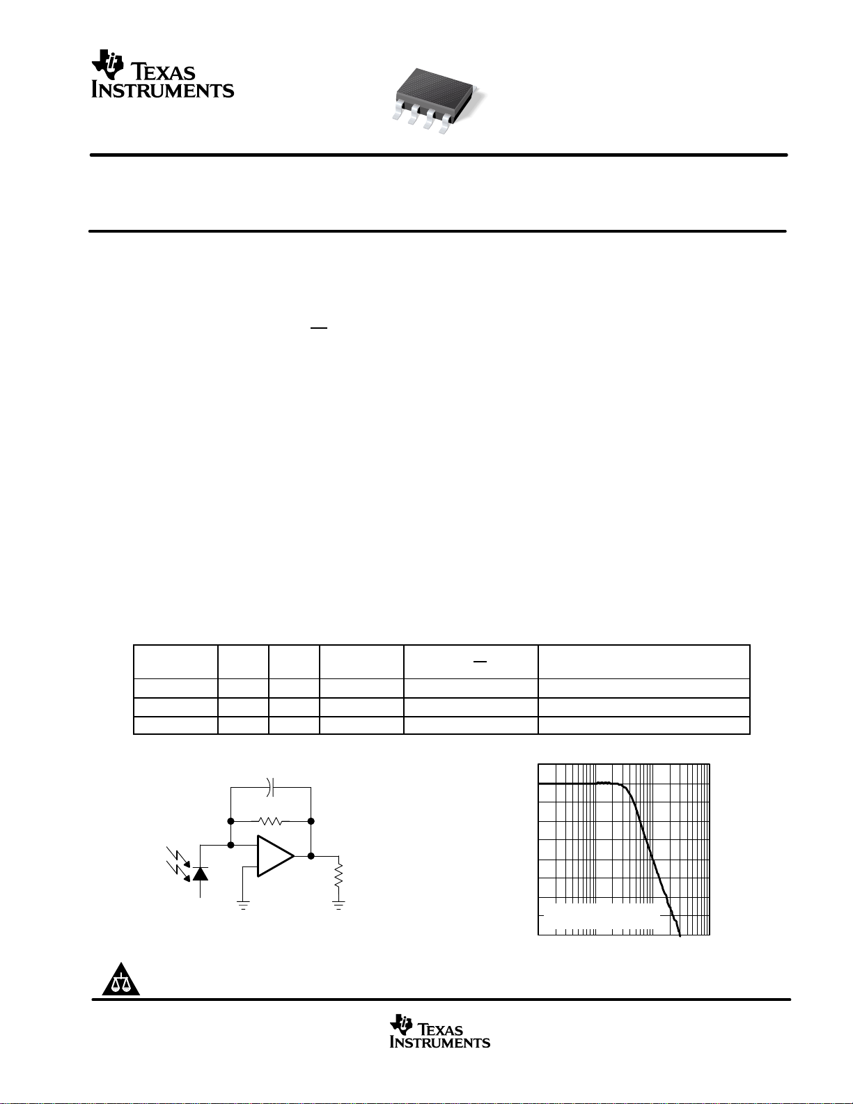
DESCRIPTION
The THS4601 is a high-speed, FET-input operational
amplifier designed for applications requiring wideband
operation, high-input impedance, and high-power
supply voltages. By providing a 180-MHz gain-
bandwidth product, ±15-V supply operation, and
100-pA input bias current, the THS4601 is capable of
wideband transimpedance gain and large output signal
swing simultaneously. Low current and voltage noise
allow amplification of extremely low-level input signals
while still maintaining a large signal-to-noise ratio.
The characteristics of the THS4601 ideally suit it for use
as a wideband photodiode amplifier. Photodiode output
current is a prime candidate for transimpedance
amplification, an application of which is illustrated in
Figure 1. Other potential applications include test and
measurement systems requiring high-input impedance,
digital-to-analog converter output buffering, high-speed
integration, and active filtering.
A SELECTION OF RELATED OPERATIONAL AMPLIFIER PRODUCTS
DEVICE
V
S
(V)
BW
(MHz)
SLEW RATE
(V/µs)
VOLTAGE NOISE
(nV√Hz
)
DESCRIPTION
OPA627
±15
16 55 4.5 Unity-gain stable FET-input amplifier
OPA637 ±15 80 135 4.5 Gain of +5 stable FET-input amplifier
OPA655 ±5 400 290 6 Unity-gain stable FET-input amplifier
_
+
THS4601
C
F
= 0.7 pF
λ
R
L
= 1 kΩ
60
65
70
75
80
85
90
95
100
105
0.1 1 10 100
Frequency – MHz
Transimpedance Gain – dB
100 kΩ TRANSIMPEDANCE BANDWIDTH
Diode Capacitance: 18 pF
–3 dB Bandwidth: 4 MHz
Figure 1. Wideband Photodiode
Transimpedance Amplifier
R
F
= 100 kΩ
–V
Bias
18 pF
PRODUCTION DATA information is current as of publication date.
Products conform to specifications per the terms of Texas Instruments
standard warranty. Production processing does not necessarily include
testing of all parameters.
Copyright 2002, Texas Instruments Incorporated
Please be aware that an important notice concerning availability, standard warranty, and use in critical applications of
Texas Instruments semiconductor products and disclaimers thereto appears at the end of this data sheet.
THS4601
SLOS388B – OCTOBER 2001 – REVISED JUNE 2002
2
www.ti.com
1
2
3
4
8
7
6
5
NC
IN–
IN+
V
S–
NC
V
S+
OUT
NC
THS4601
D AND DDA PACKAGE
(TOP VIEW)
NC – No internal connection
Terminal Functions
TERMINAL
NAME NO.
DESCRIPTION
NC 1, 5, 8 These pins have no internal connection.
IN– 2 Inverting input of the amplifier
IN+ 3 Noninverting input of the amplifier
V
S–
4 Negative power supply
OUT 6 Output of the amplifier
V
S+
7 Positive power supply
absolute maximum ratings over operating free-air temperature (unless otherwise noted)
†
Supply voltage, V
S+
16.5 V. . . . . . . . . . . . . . . . . . . . . . . . . . . . . . . . . . . . . . . . . . . . . . . . . . . . . . . . . . . . . . . . . . . . . . . . . . .
Supply voltage, V
S–
–16.5 V. . . . . . . . . . . . . . . . . . . . . . . . . . . . . . . . . . . . . . . . . . . . . . . . . . . . . . . . . . . . . . . . . . . . . . . . . .
Input voltage, V
I
±V
S
. . . . . . . . . . . . . . . . . . . . . . . . . . . . . . . . . . . . . . . . . . . . . . . . . . . . . . . . . . . . . . . . . . . . . . . . . . . . . . . . .
Output current, I
O
100 mA. . . . . . . . . . . . . . . . . . . . . . . . . . . . . . . . . . . . . . . . . . . . . . . . . . . . . . . . . . . . . . . . . . . . . . . . . . . .
Differential input voltage, V
ID
±4 V. . . . . . . . . . . . . . . . . . . . . . . . . . . . . . . . . . . . . . . . . . . . . . . . . . . . . . . . . . . . . . . . . . . . .
Maximum junction temperature, T
J
150°C. . . . . . . . . . . . . . . . . . . . . . . . . . . . . . . . . . . . . . . . . . . . . . . . . . . . . . . . . . . . . .
Operating free-air temperature, T
A:
C-suffix 0°C to 70°C. . . . . . . . . . . . . . . . . . . . . . . . . . . . . . . . . . . . . . . . . . . . . . . .
I-suffix –40°C to 85°C. . . . . . . . . . . . . . . . . . . . . . . . . . . . . . . . . . . . . . . . . . . . . . .
Storage temperature, T
stg
–65°C to 125°C. . . . . . . . . . . . . . . . . . . . . . . . . . . . . . . . . . . . . . . . . . . . . . . . . . . . . . . . . . . . . .
Lead temperature 1,6 mm (1/16 inch) from cases for 10 seconds 300°C. . . . . . . . . . . . . . . . . . . . . . . . . . . . . . . . . . . .
†
Stresses beyond those listed under “absolute maximum ratings” may cause permanent damage to the device. These are stress ratings only, and
functional operation of the device at these or any other conditions beyond those indicated under “recommended operating conditions” is not
implied. Exposure to absolute-maximum-rated conditions for extended periods may affect device reliability.
PACKAGE AND ORDERING INFORMATION
PRODUCT
PACKAGE
PACKAGE
DESIGNATOR
SPECIFIED
TEMPERATURE RANGE
PACKAGE MARKING
THS4601CD SOIC surface mount 8D 0°C to 70°C 4601C
THS4601ID SOIC surface mount 8D –40°C to 85°C 4601I
THS4601CDDA SOIC surface mount with PowerPAD 8DDA 0°C to 70°C 4601C
THS4601IDDA SOIC surface mount with PowerPAD 8DDA –40°C to 85°C 4601I
NOTE: The THS4601 is available taped and reeled. Add an R suffix to the device type when ordering (e.g., THS4601IDR).
PowerPAD is a trademark of Texas Instruments.
THS4601
SLOS388B – OCTOBER 2001 – REVISED JUNE 2002
3
www.ti.com
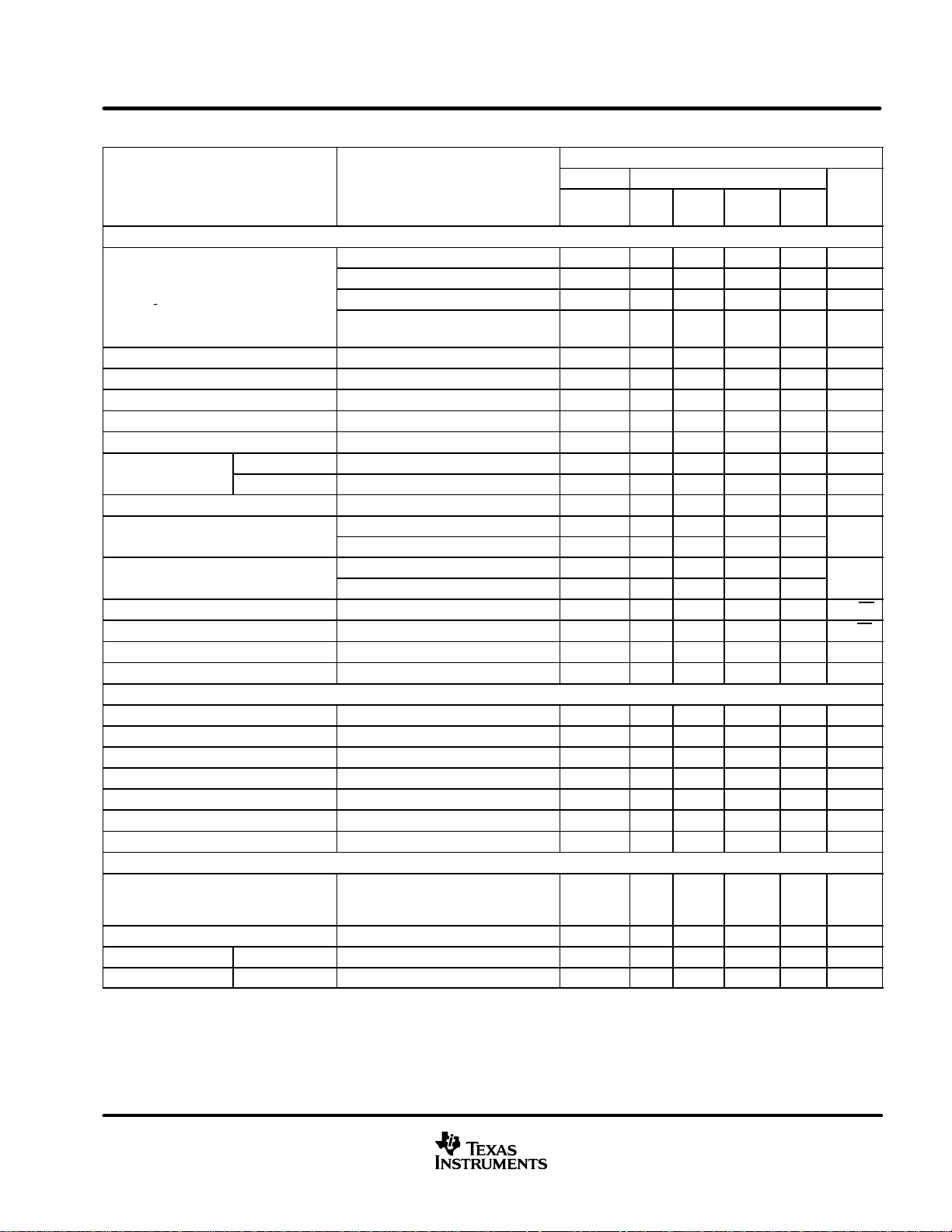
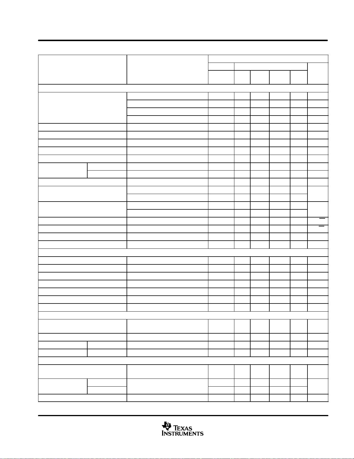
electrical specifications: V
S
= ±15 V: R
F
= 250 Ω, R
L
= 1 kΩ and G = +2 (unless otherwise noted)
THS4601
TYP OVER TEMPERATURE
PARAMETER
TEST
CONDITIONS
25°C 25°C
0°C to
70°C
–40°C
to 85°C
MIN/
MAX
UNIT
AC PERFORMANCE
G = +1, V
O
= 20 mV
pp
, R
F
= 0 Ω 440 Typ MHz
G = +2, V
O
= 40 mV
pp
, R
F
= 62 Ω 95 Typ MHz
Small-signal bandwidth
G = +5, V
O
= 100 mV
pp
, R
F
= 500 Ω 36 Typ MHz
g
G = +10, V
O
= 200 mV
pp
,
R
F
= 1 kΩ
18 Typ MHz
Gain-bandwidth product G > +10 180 Typ MHz
Bandwidth for 0.1 dB flatness G = +2, V
O
= 200 mV
pp
5 Typ MHz
Large-signal bandwidth G = +5, V
O
= 10 V
pp
3 Typ MHz
Slew rate, SR G = +5, 10 V Step 100 Typ V/µs
Rise/fall time, t
r
/t
f
1.0 V Step 7 Typ ns
0.01% G = +5, V
O
= 5 V Step 170 Typ ns
Settling time, t
s
0.1% G = +5, V
O
= 5 V Step 135 Typ ns
Harmonic distortion G = +2, f = 1 MHz, V
O
= 2V
pp
R
L
= 100 Ω –65 Typ
2
n
d
Harmonic
R
L
= 1 kΩ –77 Typ
dBc
R
L
= 100 Ω –73 Typ
3
r
d
Harmonic
R
L
= 1 kΩ –96 Typ
dBc
Input voltage noise, V
n
f > 10 kHz 5.4 Typ nV/√Hz
Input current noise, I
n
f > 10 kHz 5.5 Typ fA/√Hz
Differential gain (NTSC, P AL) G = +2, R
L
= 150 Ω 0.02% Typ
Differential phase (NTSC, P AL) G = +2, R
L
= 150 Ω 0.08 Typ _
DC PERFORMANCE
Open-loop voltage gain G = –10, R
L
= 1 kΩ 105 94 92 90 Min dB
Input offset voltage, V
IO
V
CM
= 0 V 1.0 4.0 4.5 5.0 Max mV
Average offset voltage drift V
CM
= 0 V ±10 ±10 Typ µV/_C
Input bias current, I
IB
V
CM
= 0 V 30 100 550 1100 Max pA
Average bias current drift V
CM
= 0 V 50 50 Typ pA/°C
Input offset current, I
IO
V
CM
= 0 V 2 100 200 300 Max pA
Average offset current drift V
CM
= 0 V 5 5 Typ pA/°C
INPUT
Common-mode input range, V
IC
±13.0
12.6
to
–12.0
12.5 to
–11.9
12.4 to
–11.8
Min V
Common-mode rejection ratio, CMRR 110 100 95 90 Min dB
Input impedance, Z
id
Differential 10
9
|| 3.5 Typ Ω || pF
Input impedance, Z
ic
Common-mode 10
9
|| 6.5 Typ Ω || pF
THS4601
SLOS388B – OCTOBER 2001 – REVISED JUNE 2002
4
www.ti.com
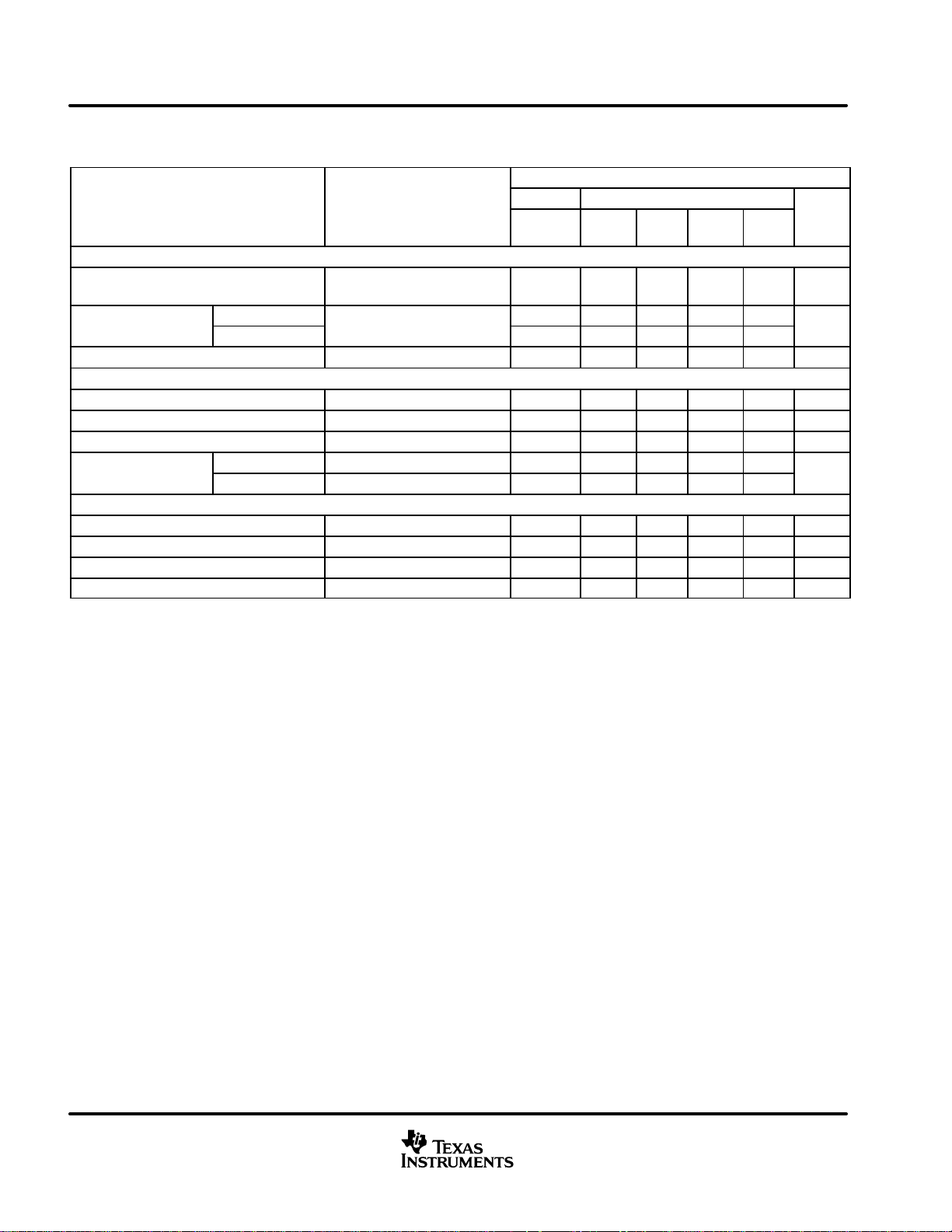
electrical specifications: V
S
= ±15 V: R
F
= 250 Ω, R
L
= 1kΩ and G = +2 (unless otherwise noted)
(continued)
THS4601
TYP OVER TEMPERATURE
PARAMETER
TEST
CONDITIONS
25°C 25°C
0°C to
70°C
–40°C
to 85°C
MIN/
MAX
UNIT
OUTPUT
Voltage output swing R
L
= 1 kΩ
12.8 to
–13.4
12.4 to
–13.1
12.3 to
–13.0
12.1 to
–12.8
Min V
Sourcing
–80 –60 –60 –59 Min
Current output, I
O
Sinking
R
L
= 20 Ω
50 35 35 34 Min
mA
Closed-loop output impedance, Z
o
G = +1, f = 1 MHz 0.1 Typ Ω
POWER SUPPLY
Specified operating voltage ±15 ±16.5 ±16.5 ±16.5 Max V
Maximum quiescent current 10.0 11.5 11.7 12.0 Max mA
Minimum quiescent current 10.0 8.5 8.3 8.0 Min mA
+PSRR 115 90 88 86 Min
Power supply rejection
–PSRR 115 90 88 86 Min
dB
TEMPERATURE
Specified operating range, T
A
–40 to 85 Typ °C
Thermal resistance, θ
JA
Junction-to-ambient
8D: SO–8 170 Typ °C/W
8DDA: SO–8 with PowerPAD 66.6 Typ °C/W
THS4601
SLOS388B – OCTOBER 2001 – REVISED JUNE 2002
5
www.ti.com
electrical specifications: V
S
= ±5 V: R
F
= 250 Ω, R
L
= 1 kΩ and G = +2 (unless otherwise noted)
THS4601
TYP OVER TEMPERATURE
PARAMETER
TEST
CONDITIONS
25°C 25°C
0°C to
70°C
–40°C
to 85°C
MIN/
MAX
UNIT
AC PERFORMANCE
G = +1, V
O
= 20 mV
pp
400 Typ MHz
G = +2, V
O
= 40 mV
pp
100 Typ MHz
Small-signal bandwidth
G = +5, V
O
= 100 mV
pp
50 Typ MHz
G = +10, V
O
= 200 mV
pp
18 Typ MHz
Gain-bandwidth product G > +10 180 Typ MHz
Bandwidth for 0.1 dB flatness G = +2, V
O
= 200 mV
pp
5 Typ MHz
Large-signal bandwidth G = +5, V
O
= 5 V
pp
6 Typ MHz
Slew rate, SR G = +5, 5 V Step 100 Typ V/µs
Rise/fall time, t
r
/t
f
1.0 V Step 8 Typ ns
0.01% G = +5, V
O
= 2 V Step 140 Typ ns
Settling time, t
s
0.1% G = +5, V
O
= 2 V Step 170 Typ ns
Harmonic distortion G = +2, f = 1 MHz, V
O
= 2V
pp
R
L
= 100 Ω –74 Typ
2
n
d
Harmonic
R
L
= 1 kΩ –84 Typ
dBc
R
L
= 100 Ω –79 Typ
3
r
d
Harmonic
R
L
= 1 kΩ –94 Typ
dBc
Input voltage noise, V
n
f > 10 kHz 5.4 Typ nV/√Hz
Input current noise, I
n
f > 10 kHz 5.5 Typ fA/√Hz
Differential gain (NTSC and P AL) G = +2, R
L
= 150 Ω 0.02% Typ
Differential phase (NTSC and P AL) G = +2, R
L
= 150 Ω 0.08 Typ _
DC PERFORMANCE
Open-loop voltage gain G = –10, R
L
= 1 kΩ 105 94 92 90 Min dB
Input offset voltage, V
IO
V
CM
= 0 V 1.0 4.0 4.5 5.0 Max mV
Average offset voltage drift V
CM
= 0 V ±10 ±10 Typ µV/_C
Input bias current, I
IB
V
CM
= 0 V 20 100 550 1100 Max pA
Average bias current drift V
CM
= 0 V 50 50 Typ pA/°C
Input offset current, I
IO
V
CM
= 0 V 1 100 200 300 Max pA
Average offset current drift V
CM
= 0 V 5 5 Typ pA/°C
INPUT
Common-mode input range, V
IC
±2.2
2.7 to
–2.0
2.6 to
–1.9
2.5 to
–1.8
Min V
Common-mode rejection ratio, CMRR 110 100 95 90 Min dB
Input impedance, Z
id
Differential 10
9
|| 3.5 Typ Ω || pF
Input impedance, Z
ic
Common-mode 10
9
|| 6.5 Typ Ω || pF
OUTPUT
Voltage output swing R
L
= 1 kΩ
2.9 to
–3.5
2.6 to
–3.3
2.5 to
–3.2
2.3 to
–3.1
Min V
Sourcing
–65 –48 –48 –47 Min
Current output, I
O
Sinking
R
L
= 20 Ω
45 30 30 29 Min
mA
Closed-loop output impedance, Z
o
G = +1, f = 1 MHz 0.1 Typ Ω
THS4601
SLOS388B – OCTOBER 2001 – REVISED JUNE 2002
6
www.ti.com
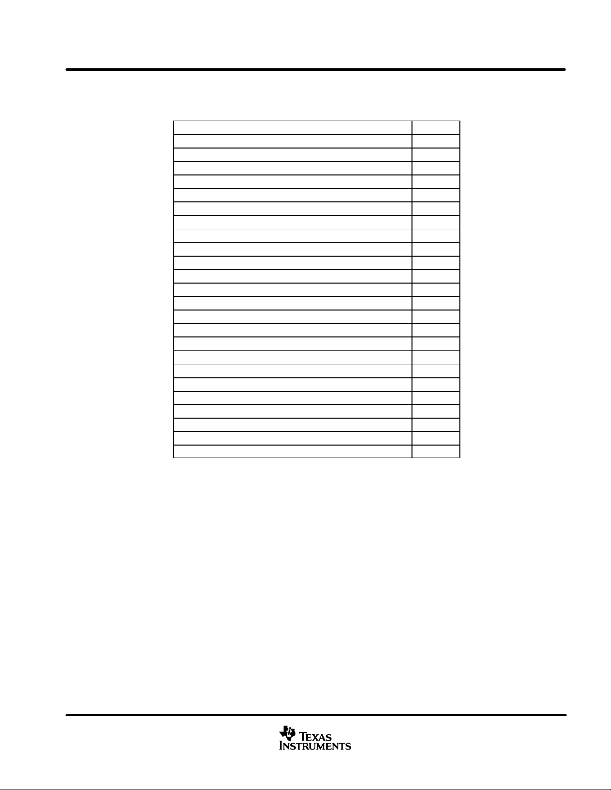
electrical specifications: V
S
= ±5 V; R
F
= 250 Ω, R
L
= 1 kΩ and G = +2 (unless otherwise noted)
(continued)
THS4601
TYP OVER TEMPERATURE
PARAMETER
TEST
CONDITIONS
25°C 25°C
0°C to
70°C
–40°C
to 85°C
MIN/
MAX
UNIT
POWER SUPPLY
Specified operating voltage ±5 ±16.5 ±16.5 ±16.5 Max V
Maximum quiescent current 9.6 11.2 11.4 11.7 Max mA
Minimum quiescent current 9.6 8.2 8.0 7.7 Min mA
+PSRR 110 90 88 86 Min
Power supply rejection
–PSRR 110 90 88 86 Min
dB
TEMPERATURE
Specified operating range, T
A
–40 to 85 Typ °C
Thermal resistance, θ
JA
Junction-to-ambient
8D: SO–8 170 Typ °C/W
8DDA: SO–8 with PowerPAD 67 Typ °C/W
THS4601
SLOS388B – OCTOBER 2001 – REVISED JUNE 2002
7
www.ti.com
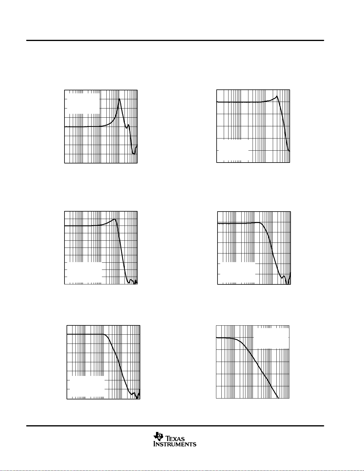
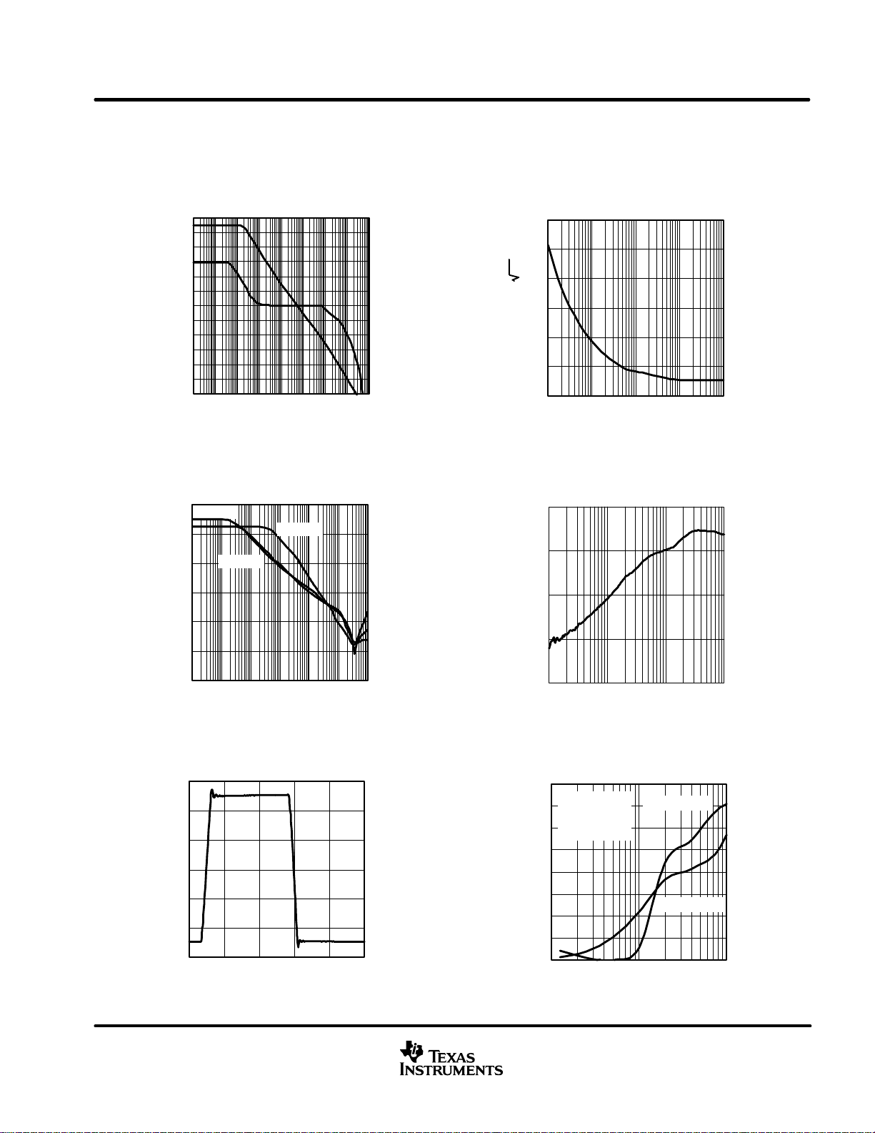
TYPICAL CHARACTERISTICS
Table of Graphs
FIGURE
Small-Signal Unity Gain Frequency Response 2
Large-Signal Unity Gain Frequency Response 3
Small-Signal Frequency Response, Gain = +2 4
Small-Signal Frequency Response, Gain = +5 5
Small-Signal Frequency Response, Gain = +10 6
Small-Signal Frequency Response, Gain = +100 7
Open-Loop Gain and Phase vs Frequency 8
Voltage Noise vs Frequency 9
Rejection Ratios vs Frequency 10
Closed-Loop Output Impedance vs Frequency 11
Large-Signal Pulse Response 12
Harmonic Distortion vs Frequency 13
Harmonic Distortion vs Output Voltage Swing 14
Slew Rate vs Output Voltage Step 15
Input Bias Current vs Input Common-Mode Range 16
Common-Mode Rejection Ratio vs Input Common-Mode Range 17
Open-Loop Gain vs Temperature 18
Input Bias Current vs Temperature 19
Input Offset Current vs Temperature 20
Offset Voltage vs Temperature 21
Quiescent Current vs Temperature 22
Output Current vs Temperature 23
Output Voltage Swing vs Temperature 24
Rejection Ratios vs Temperature 25
THS4601
SLOS388B – OCTOBER 2001 – REVISED JUNE 2002
8
www.ti.com
TYPICAL CHARACTERISTICS
measurement conditions: T
A
= 25°C, R
L
= 1 kΩ, V
S
= ±15 V (unless otherwise noted)
Figure 2
–8
–6
–4
–2
0
2
4
6
8
100 k 1 M 10 M 100 M 1 G
Gain – dB
Frequency – Hz
SMALL-SIGNAL UNITY GAIN
FREQUENCY RESPONSE
Gain = 1,
R
F
= 0Ω,
R
L
= 1 kΩ,
P
IN
= –30 dBm
Figure 3
–25
–20
–15
–10
–5
0
5
100 k 1 M 10 M 100 M
Gain – dB
LARGE-SIGNAL UNITY GAIN
FREQUENCY RESPONSE
Gain = 1,
R
F
= 0 Ω,
R
L
= 1 kΩ,
P
IN
= 0 dBm
Frequency – Hz
Figure 4
–10
–8
–6
–4
–2
0
2
4
6
8
10
100 k 1 M 10 M 100 M 1 G
Gain – dB
Frequency – Hz
SMALL-SIGNAL FREQUENCY RESPONSE,
GAIN = +2
Gain = 2,
R
F
= 62Ω,
R
L
= 1 kΩ,
P
IN
= –30 dBm
Figure 5
–15
–10
–5
0
5
10
15
20
100 k 1 M 10 M 100 M 1 G
Gain – dB
Frequency – Hz
SMALL-SIGNAL FREQUENCY RESPONSE,
GAIN = +5
Gain = 5,
R
F
= 500Ω,
R
L
= 1 kΩ,
P
IN
= –30 dBm
Figure 6
–15
–10
–5
0
5
10
15
20
25
100 k 1 M 10 M 100 M 1 G
Gain – dB
Frequency – Hz
SMALL-SIGNAL FREQUENCY RESPONSE,
GAIN = +10
Gain = 10,
R
F
= 1 kΩ,
R
L
= 1 kΩ,
P
IN
= –30 dBm
Figure 7
–10
0
10
20
30
40
50
100 k 1 M 10 M 100 M 1 G
Gain – dB
Frequency – Hz
SMALL-SIGNAL FREQUENCY RESPONSE,
GAIN = +100
Gain = 100,
R
F
= 5 kΩ,
R
L
= 1 kΩ,
P
IN
= –30 dBm
THS4601
SLOS388B – OCTOBER 2001 – REVISED JUNE 2002
9
www.ti.com
TYPICAL CHARACTERISTICS
measurement conditions: T
A
= 25°C, R
L
= 1 kΩ, V
S
= ±15 V (unless otherwise noted)
Figure 8
–10
0
10
20
30
40
50
60
70
80
90
100
110
10 100 1 k 10 k 100 k 1 M 10 M 100 M 1 G
–270
–240
–210
–180
–150
–120
–90
–60
–30
0
30
60
90
Frequency – Hz
Gain – dB
OPEN-LOOP GAIN AND PHASE
vs
FREQUENCY
Phase – °
Figure 9
0
10
20
30
40
50
60
10 100 1 k 10 k 100 k
Frequency – Hz
Voltage Noise –
VOLTAGE NOISE
vs
FREQUENCY
nV/ Hz
Figure 10
0
20
40
60
80
100
120
100 1 k 10 k 100 k 1 M
10 M 100 M
Rejection Ratio – dB
REJECTION RATIOS
vs
FREQUENCY
CMRR
PSRR+
PSRR–
Frequency – Hz
Figure 11
0.01
0.1
1
10
100
100 k 1 M 10 M 100 M
Frequency – Hz
Output Impedance –
CLOSED-LOOP OUTPUT IMPEDANCE
vs
FREQUENCY
Ω
Figure 12
–3
–2
–1
0
1
2
3
0 0.2 0.4 0.6 0.8 1
t – Time – µs
Output Voltage – V
LARGE-SIGNAL PULSE RESPONSE
Figure 13
–100
–90
–80
–70
–60
–50
–40
–30
–20
100 k 1 M 10 M
Frequency – Hz
Distortion – dBc
HARMONIC DISTORTION
vs
FREQUENCY
2nd Harmonic
3rd Harmonic
Gain = 2,
R
F
= 250 Ω,
R
L
= 1 kΩ,
V
O
= 2 V
PP
 Loading...