


THS4062EVM
THS4061, THS4062
180-MHz HIGH-SPEED AMPLIFIERS
SLOS234D – DECEMBER 1998 – REVISED FEBRUARY 2000
1
POST OFFICE BOX 655303 • DALLAS, TEXAS 75265
D
High Speed
– 180 MHz Bandwidth (G = 1, –3 dB)
– 400 V/µs Slew Rate
– 40-ns Settling Time (0.1%)
D
High Output Drive, IO = 115 mA (typ)
D
Excellent Video Performance
– 75 MHz 0.1 dB Bandwidth (G = 1)
– 0.02% Differential Gain
– 0.02° Differential Phase
D
Very Low Distortion
– THD = –72 dBc at f = 1 MHz
D
Wide Range of Power Supplies
– VCC = ±5 V to ±15 V
D
Available in Standard SOIC, MSOP
PowerPAD, JG, or FK Package
D
Evaluation Module Available
description
The THS4061 and THS4062 are generalpurpose, single/dual, high-speed voltage feedback amplifiers ideal for a wide range of
applications including video, communication, and
imaging. The devices offer very good ac
performance with 180-MHz bandwidth, 400-V/µs
slew rate, and 40-ns settling time (0.1% ). The
THS4061/2 are stable at all gains for both
inverting and noninverting configurations. These
amplifiers have a high output drive capability of
1 15 mA and draw only 7.8 mA supply current per
channel. Excellent professional video results can
be obtained with the low differential gain/phase
errors of 0.02%/0.02° and wide 0.1 db flatness to
75 MHz. For applications requiring low distortion,
the THS4061/2 is ideally suited with total
harmonic distortion of –72 dBc at f = 1 MHz.
PowerPAD is a trademark of Texas Insruments Incorporated.
Copyright 2000, Texas Instruments Incorporated
PRODUCTION DATA information is current as of publication date.
Products conform to specifications per the terms of Texas Instruments
standard warranty. Production processing does not necessarily include
testing of all parameters.
Please be aware that an important notice concerning availability, standard warranty, and use in critical applications of
Texas Instruments semiconductor products and disclaimers thereto appears at the end of this data sheet.
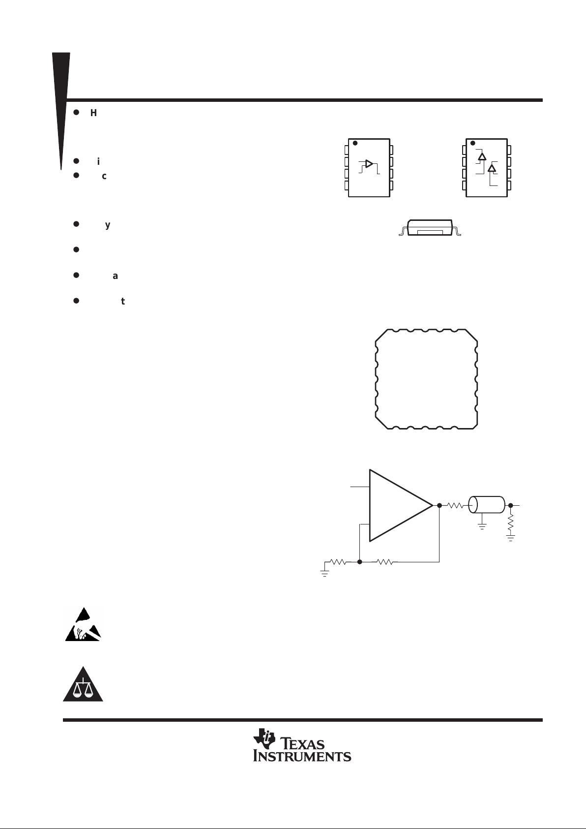
THS4062
D AND DGN PACKAGE
(TOP VIEW)
1
2
3
4
8
7
6
5
1OUT
1IN–
1IN+
–V
CC
V
CC+
2OUT
2IN–
2IN+
1
2
3
4
8
7
6
5
NULL
IN–
IN+
V
CC–
NULL
V
CC+
OUT
NC
THS4061
JG, D AND DGN PACKAGE
(TOP VIEW)
NC – No internal connection
_
+
THS4061
2 kΩ
V
I
2 kΩ
75 Ω
75 Ω
V
O
75 Ω
LINE DRIVER (G = 2)
Cross-Section View Showing
PowerPAD Option (DGN)
1920132
17
18
16
15
14
1312119 10
5
4
6
7
8
NC
V
CC+
NC
OUT
NC
NC
IN–
NC
IN+
NC
NC
NULLNCNULL
NC
V
NCNCNC
NC
THS4061
FK PACKAGE
(TOP VIEW)
CC–
On products compliant to MIL-PRF-38535, all parameters are tested
unless otherwise noted. On all other products, production
processing does not necessarily include testing of all parameters.
CAUTION: The THS4061 and THS4062 provide ESD protection circuitry. However , permanent damage can still occur if this
device is subjected to high-energy electrostatic discharges. Proper ESD precautions are recommended to avoid any
performance degradation or loss of functionality
THS4061, THS4062
180-MHz HIGH-SPEED AMPLIFIERS
SLOS234D – DECEMBER 1998 – REVISED FEBRUARY 2000
2
POST OFFICE BOX 655303 • DALLAS, TEXAS 75265
RELATED DEVICES
DEVICE DESCRIPTION
THS4011/2
THS4031/2
THS4061/2
290-MHz Low Distortion High-Speed Amplifiers
100-MHz Low Noise High Speed-Amplifiers
180-MHz High-Speed Amplifiers
AVAILABLE OPTIONS
PACKAGED DEVICES
T
A
NUMBER OF
CHANNELS
PLASTIC
SMALL
OUTLINE
†
(D)
PLASTIC
MSOP
†
(DGN)
CERAMIC
DIP
(JG)
CHIP
CARRIER
(FK)
MSOP
SYMBOL
EVALUATION
MODULES
0°C to
1 THS4061CD THS4061CDGN — — TIABS THS4061EVM
70°C
2 THS4062CD THS4062CDGN — — TIABM THS4062EVM
–40°C to
1 THS4061ID THS4061IDGN — — TIABT —
85°C
2 THS4062ID THS4062IDGN — — TIABN —
–55°C to
125°C
1 — — THS4061MJG THS4061MFK — —
†
The D and DGN packages are available taped and reeled. Add an R suffix to the device type (i.e., THS4061CDGNR).
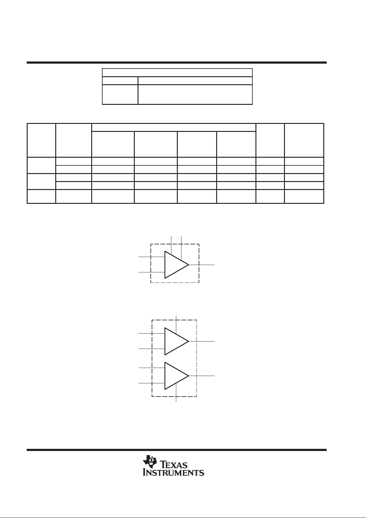
functional block diagram
OUT
8
6
1
IN–
IN+
2
3
Null
–
+
Figure 1. THS4061 – Single Channel
1OUT
1IN–
1IN+
V
CC
2OUT
2IN–
2IN+
–V
CC
8
6
1
2
3
5
7
4
–
+
–
+
Figure 2. THS4062 – Dual Channel
THS4061, THS4062
180-MHz HIGH-SPEED AMPLIFIERS
SLOS234D – DECEMBER 1998 – REVISED FEBRUARY 2000
3
POST OFFICE BOX 655303 • DALLAS, TEXAS 75265
absolute maximum ratings over operating free-air temperature (unless otherwise noted)
†
Supply voltage, VCC+ to VCC– 33 V. . . . . . . . . . . . . . . . . . . . . . . . . . . . . . . . . . . . . . . . . . . . . . . . . . . . . . . . . . . . . .
Input voltage, VI ±V
CC
. . . . . . . . . . . . . . . . . . . . . . . . . . . . . . . . . . . . . . . . . . . . . . . . . . . . . . . . . . . . . . . . . . . . . . . . . .
Output current, IO 150 mA. . . . . . . . . . . . . . . . . . . . . . . . . . . . . . . . . . . . . . . . . . . . . . . . . . . . . . . . . . . . . . . . . . . . . . .
Differential input voltage, V
IO
±4 V. . . . . . . . . . . . . . . . . . . . . . . . . . . . . . . . . . . . . . . . . . . . . . . . . . . . . . . . . . . . . . . .
Continuous total power dissipation See Dissipation Rating Table. . . . . . . . . . . . . . . . . . . . . . . . . . . . . . . . . . . . .
Maximum junction temperature, TJ 150°C. . . . . . . . . . . . . . . . . . . . . . . . . . . . . . . . . . . . . . . . . . . . . . . . . . . . . . . . .
Operating free-air temperature, TA: C-suffix 0°C to 70°C. . . . . . . . . . . . . . . . . . . . . . . . . . . . . . . . . . . . . . . . . . .
I-suffix –40°C to 85°C. . . . . . . . . . . . . . . . . . . . . . . . . . . . . . . . . . . . . . . . . .
M-suffix –55°C to 125°C. . . . . . . . . . . . . . . . . . . . . . . . . . . . . . . . . . . . . . . .
Storage temperature, T
stg
–65°C to 150°C. . . . . . . . . . . . . . . . . . . . . . . . . . . . . . . . . . . . . . . . . . . . . . . . . . . . . . . . .
Lead temperature 1,6 mm (1/16 inch) from case for 10 seconds, D and DGN package 300°C. . . . . . . . . . . .
Lead temperature 1,6 mm (1/16 inch) from case for 60 seconds, JG package 300°C. . . . . . . . . . . . . . . . . . . .
Case temperature for 60 seconds, FK package 260°C. . . . . . . . . . . . . . . . . . . . . . . . . . . . . . . . . . . . . . . . . . . . . .
†
Stresses beyond those listed under “absolute maximum ratings” may cause permanent damage to the device. These are stress ratings only and
functional operation of the device at these or any other conditions beyond those indicated under “recommended operating conditions” is not
implied. Exposure to absolute-maximum-rated conditions for extended periods may affect device reliability.
DISSIPATION RATING TABLE
T
≤ 25°C DERATING FACTOR T
= 70°C T
= 85°C T
= 125°C
PACKAGE
A
POWER RATING ABOVE TA = 25°C
A
POWER RATING
A
POWER RATING
A
POWER RATING
D 740 mW 6 mW/°C 475 mW 385 mW —
DGN
‡
2.14 W 17.1 mW/°C 1.37 W 1.11 W —
JG 1057 mW 8.4 mW/°C 627 mW 546 mW 210 mW
FK 1375 mW 11 mW/°C 880 mW 715 mW 275 mW
‡
The DGN package incorporates a PowerPAD on the underside of the device. This acts as a heatsink and must be connected to a thermal dissipation
plane for proper power dissipation. Failure to do so can result in exceeding the maximum specified junction temperature, which could permanently
damage the device.
recommended operating conditions
MIN NOM MAX UNIT
pp
Dual supply ±4.5 ±16
Suppl
y v
oltage, V
CC
+
and V
CC
–
Single supply 9 32
V
C-suffix 0 70
Operating free-air temperature, T
A
I-suffix –40 85
°C
M-suffix –55 125
THS4061, THS4062
180-MHz HIGH-SPEED AMPLIFIERS
SLOS234D – DECEMBER 1998 – REVISED FEBRUARY 2000
4
POST OFFICE BOX 655303 • DALLAS, TEXAS 75265
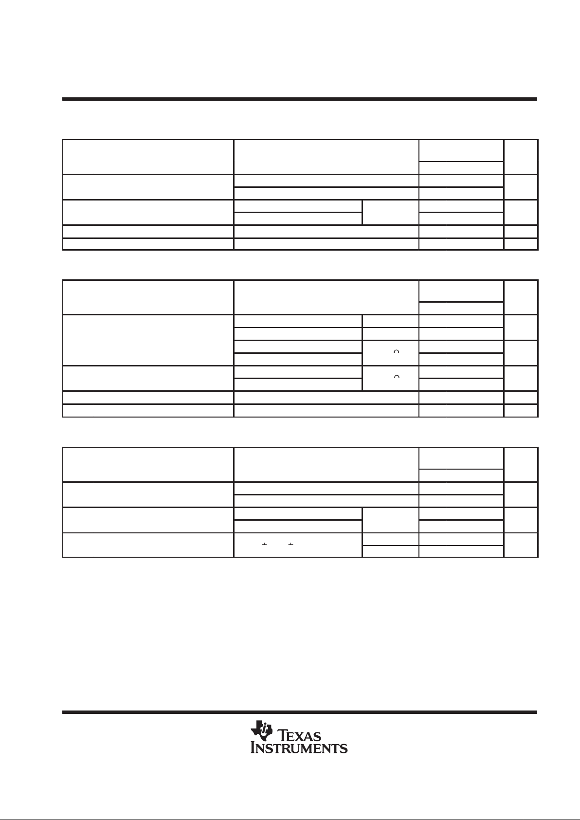
electrical characteristics at TA = 25°C, VCC = ±15 V, RL = 150 Ω (unless otherwise noted)
dynamic performance
PARAMETER
TEST CONDITIONS
†
THS4061C/I,
THS4062C/I
UNIT
MIN TYP MAX
VCC = ±5 V Gain = 1 180 MHz
Dynamic performance small-signal
–
VCC = ±15 V
50
BW
bandwidth (–3 dB)
VCC = ±5 V
Gain
= –
1
50
MH
z
VCC = ±15 V
75
Bandwidth for 0.1 dB flatness
VCC = ±5 V
Gain
=
1
20
MH
z
VCC = ±15 V
400
SR
Slew rate
VCC = ±5 V
Gain
= –
1
350
V/µs
VCC = ±15 V, 5-V step (0 V to 5 V)
40
Settling time to 0.1%
VCC = ±5 V, VO = –2.5 V to 2.5 V,
Gain
= –
1
40
ns
t
s
VCC = ±15 V, 5-V step (0 V to 5 V)
140
Settling time to 0.01%
VCC = ±5 V, VO = –2.5 V to 2.5 V,
Gain
= –
1
150
ns
†
Full range = 0°C to 70°C for C suffix and –40°C to 85°C for I suffix
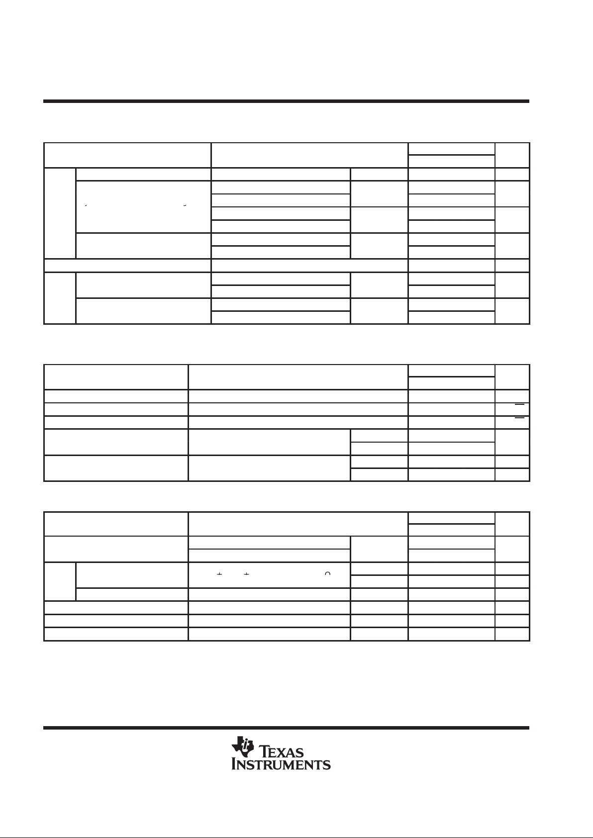
noise/distortion performance
PARAMETER
TEST CONDITIONS
†
THS4061C/I,
THS4062C/I
UNIT
MIN TYP MAX
THD Total harmonic distortion f = 1 MHz –72 dBc
V
n
Input voltage noise f = 10 kHz, VCC = ±5 V or ±15 V 14.5 nV/√Hz
I
n
Input current noise f = 10 kHz, VCC = ±5 V or ±15 V 1.6 pA/√Hz
VCC = ±15 V
0.02
%
Differential gain error
Gain
= 2,
NTSC
, 40
IRE modulation
VCC = ±5 V
0.02
%
p
VCC = ±15 V 0.02°
Differential phase error
Gain
= 2,
NTSC
, 40
IRE modulation
VCC = ±5 V 0.06°
Channel-to-channel crosstalk
(THS4062 only)
VCC = ±5 V or ±15 V, f = 1 MHz 65 dB
†
Full range = 0°C to 70°C for C suffix and –40°C to 85°C for I suffix
dc performance
PARAMETER
TEST CONDITIONS
†
THS4061C/I,
THS4062C/I
UNIT
MIN TYP MAX
TA = 25°C 5 15
p
p
V
CC
=
±15 V,V
O
=
±10 V
,
R
L
=
1 kΩ
TA = full range 4
V/mV
Open loop gain
TA = 25°C 2.5 8
V
CC
= ±5 V,
V
O
= ±2.5 V,
R
L
= 1
kΩ
TA = full range 2
V/mV
Input offset voltage VCC = ±5 V or ±15 V
2.5 8 mV
V
OS
Offset drift VCC = ±5 V or ±15 V
T
A
=
full range
15 µV/°C
I
IB
Input bias current VCC = ±5 V or ±15 V TA = full range 3 6 µA
I
OS
Input offset current VCC = ±5 V or ±15 V TA = full range 75 250 nA
Offset current drift TA = full range 0.3 nA/°C
†
Full range = 0°C to 70°C for C suffix and –40°C to 85°C for I suffix
THS4061, THS4062
180-MHz HIGH-SPEED AMPLIFIERS
SLOS234D – DECEMBER 1998 – REVISED FEBRUARY 2000
5
POST OFFICE BOX 655303 • DALLAS, TEXAS 75265
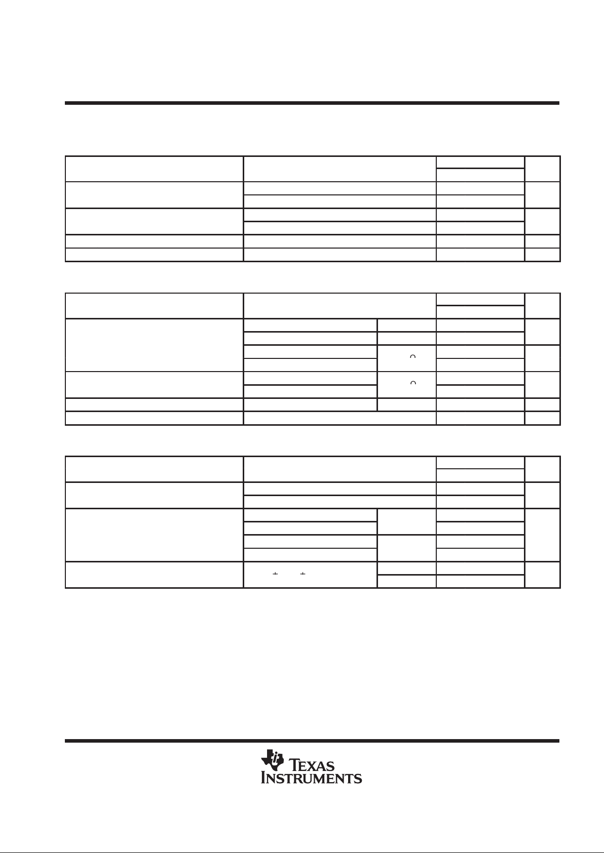
electrical characteristics at TA = 25°C, VCC = ±15 V , RL = 150 Ω (unless otherwise noted) (continued)
input characteristics
PARAMETER
TEST CONDITIONS
†
THS4061C/I,
THS4062C/I
UNIT
MIN TYP MAX
p
VCC = ±15 V ±13.8 ±14.1
V
ICR
Common-mode input voltage range
VCC = ±5 V ±3.8 ±4.3
V
VCC = ±15 V , V
ICR
= ±12 V
70 110
CMRR
Common mode rejection ratio
VCC = ±5 V, V
ICR
= ±2.5 V
T
A
=
full range
70 95
dB
R
I
Input resistance 1 MΩ
C
i
Input capacitance 2 pF
†
Full range = 0°C to 70°C for C suffix and –40°C to 85°C for I suffix
output characteristics
PARAMETER
TEST CONDITIONS
†
THS4061C/I,
THS4062C/I
UNIT
MIN TYP MAX
VCC = ±15 V RL = 250 Ω ±11.5 ±12.5
p
VCC = ±5 V RL = 150 Ω ±3.2 ±3.5
V
VOOutput voltage swing
VCC = ±15 V
±13 ±13.5
VCC = ±5 V
R
L
= 1
kΩ
±3.5 ±3.7
V
p
VCC = ±15 V
80 115
IOOutput current
VCC = ±5 V
R
L
= 20
Ω
50 75
mA
I
SC
Short-circuit current VCC = ±15 V 150 mA
R
O
Output resistance Open loop 12 Ω
†
Full range = 0°C to 70°C for C suffix and –40°C to 85°C for I suffix
power supply
PARAMETER
TEST CONDITIONS
†
THS4061C/I,
THS4062C/I
UNIT
MIN TYP MAX
pp
p
Dual supply ±4.5 ±16.5
VCCSuppl
y v
oltage operating range
Single supply 9 33
V
p
p
VCC = ±15 V
7.8 10.5
ICCQuiescent current (per amplifier)
VCC = ±5 V
T
A
=
full range
7.3 10
mA
pp
TA = 25°C 70 78
PSRR
Power supply rejection ratio
V
CC
= ±5 V or
±15 V
TA = full range 68
dB
†
Full range = 0°C to 70°C for C suffix and –40°C to 85°C for I suffix
THS4061, THS4062
180-MHz HIGH-SPEED AMPLIFIERS
SLOS234D – DECEMBER 1998 – REVISED FEBRUARY 2000
6
POST OFFICE BOX 655303 • DALLAS, TEXAS 75265
electrical characteristics at TA = 25°C, VCC = ±15 V, RL = 150 Ω (unless otherwise noted)
dynamic performance
THS4061M
PARAMETER
TEST CONDITIONS
†
MIN TYP MAX
UNIT
Unity-gain bandwidth Closed loop, RL = 1 kΩ VCC = ±15 V *140 180 MHz
VCC = ±15 V
180
Dynamic performance small-signal
VCC = ±5 V
Gain
=
1
180
MH
z
BW
yg
bandwidth (–3 dB)
VCC = ±15 V
50
VCC = ±5 V
Gain
= –
1
50
MH
z
VCC = ±15 V
75
Bandwidth for 0.1 dB flatness
VCC = ±5 V
Gain
=
1
20
MH
z
SR Slew rate VCC = ±15 V RL = 1 kΩ *400 500 V/µs
VCC = ±15 V, 5-V step (0 V to 5 V)
40
Settling time to 0.1%
VCC = ±5 V, VO = –2.5 V to 2.5 V,
Gain
= –
1
40
ns
t
s
VCC = ±15 V, 5-V step (0 V to 5 V)
140
Settling time to 0.01%
VCC = ±5 V, VO = –2.5 V to 2.5 V,
Gain
= –
1
150
ns
†
Full range = –55°C to 125°C for M suffix
*This parameter is not tested.
noise/distortion performance
THS4061M
PARAMETER
TEST CONDITIONS
†
MIN TYP MAX
UNIT
THD Total harmonic distortion f = 1 MHz –72 dBc
V
n
Input voltage noise f = 10 kHz, VCC = ±5 V or ±15 V 14.5 nV/√Hz
I
n
Input current noise f = 10 kHz, VCC = ±5 V or ±15 V 1.6 pA/√Hz
VCC = ±15 V 0.02
Differential gain error
Gain
= 2,
NTSC
, 40
IRE Modulation
VCC = ±5 V 0.02
%
p
VCC = ±15 V 0.02°
Differential phase error
Gain
= 2,
NTSC
, 40
IRE Modulation
VCC = ±5 V 0.06°
†
Full range = –55°C to 125°C for M suffix
dc performance
THS4061M
PARAMETER
TEST CONDITIONS
†
MIN TYP MAX
UNIT
p
p
VCC = ±15 V , VO = ±10 V, RL = 1 kΩ
5 9
Open loop gain
VCC = ±5 V, VO = ±2.5 V, RL = 1 kΩ
T
A
= full
range
2.5 6
V/mV
p
TA = 25°C 2.5 8 mV
V
IO
Input offset voltage
V
CC
=
±5 V or ±15 VR
L
=
1 kΩ
TA = full range 9 mV
Offset drift VCC = ±5 V or ±15 V RL = 1 kΩ TA = full range 15 µV/°C
I
IB
Input bias current VCC = ±5 V or ±15 V RL = 1 kΩ TA = full range 3 6 µA
I
IO
Input offset current VCC = ±5 V or ±15 V RL = 1 kΩ TA = full range 75 250 nA
Offset current drift VCC = ±5 V or ±15 V RL = 1 kΩ TA = full range 0.3 nA/°C
†
Full range = –55°C to 125°C for M suffix
THS4061, THS4062
180-MHz HIGH-SPEED AMPLIFIERS
SLOS234D – DECEMBER 1998 – REVISED FEBRUARY 2000
7
POST OFFICE BOX 655303 • DALLAS, TEXAS 75265
electrical characteristics at TA = full range, VCC = ±15 V, RL = 1 kΩ (unless otherwise noted)
(continued)
input characteristics
THS4061M
PARAMETER
TEST CONDITIONS
†
MIN TYP MAX
UNIT
p
VCC = ±15 V ±13.8 ±14.1
V
ICR
Common-mode input voltage range
VCC = ±5 V ±3.8 ±4.3
V
VCC = ±15 V , V
ICR
= ±12 V 70 86
CMRR
Common mode rejection ratio
VCC = ±5 V, V
ICR
= ±2.5 V 80 90
dB
R
I
Input resistance 1 MΩ
C
i
Input capacitance 2 pF
†
Full range = –55°C to 125°C for M suffix
output characteristics
THS4061M
PARAMETER
TEST CONDITIONS
†
MIN TYP MAX
UNIT
VCC = ±15 V RL = 250 Ω ±12 ±13.1
p
VCC = ±5 V RL = 150 Ω ±3.2 ±3.5
V
VOOutput voltage swing
VCC = ±15 V
±13 ±13.5
VCC = ±5 V
R
L
= 1
kΩ
±3.5 ±3.7
V
p
VCC = ±15 V
70 115
IOOutput current
VCC = ±5 V
R
L
= 20
Ω
50 75
mA
I
SC
Short-circuit current VCC = ±15 V TA = 25°C 150 mA
R
O
Output resistance Open loop 12 Ω
†
Full range = –55°C to 125°C for M suffix
power supply
THS4061M
PARAMETER
TEST CONDITIONS
†
MIN TYP MAX
UNIT
pp
p
Dual supply ±4.5 ±16.5
VCCSuppl
y v
oltage operating range
Single supply 9 33
V
VCC = ±15 V
°
7.8 9
VCC = ±5 V
T
A
=
25°C
7.3 8.5
ICCQuiescent current
VCC = ±15 V
11
mA
VCC = ±5 V
T
A
= full
range
10.5
pp
TA = 25°C 76 80
PSRR
Power supply rejection ratio
V
CC
= ±5 V or
±15 V
TA = full range 74 78
dB
†
Full range = –55°C to 125°C for M suffix
 Loading...