


MOTOROLA MC74HC373ADT, MC74HC373ADTEL, MC74HC373ADTR2, MC74HC373AH, MC74HC373AFR1 Datasheet
...
MC74HC373A
Octal 3-State Non-Inverting
Transparent Latch
High±Performance Silicon±Gate CMOS
The MC74HC373A is identical in pinout to the LS373. The device inputs are compatible with standard CMOS outputs; with pullup resistors, they are compatible with LSTTL outputs.
These latches appear transparent to data (i.e., the outputs change asynchronously) when Latch Enable is high. When Latch Enable goes low, data meeting the setup and hold time becomes latched.
The Output Enable input does not affect the state of the latches, but when Output Enable is high, all device outputs are forced to the high±impedance state. Thus, data may be latched even when the outputs are not enabled.
The HC373A is identical in function to the HC573A which has the data inputs on the opposite side of the package from the outputs to facilitate PC board layout.
The HC373A is the non±inverting version of the HC533A.
•Output Drive Capability: 15 LSTTL Loads
•Outputs Directly Interface to CMOS, NMOS and TTL
•Operating Voltage Range: 2.0 to 6.0 V
•Low Input Current: 1.0 μA
•High Noise Immunity Characteristic of CMOS Devices
•In Compliance with the Requirements Defined by JEDEC Standard No. 7A
•Chip Complexity: 186 FETs or 46.5 Equivalent Gates
http://onsemi.com
|
|
|
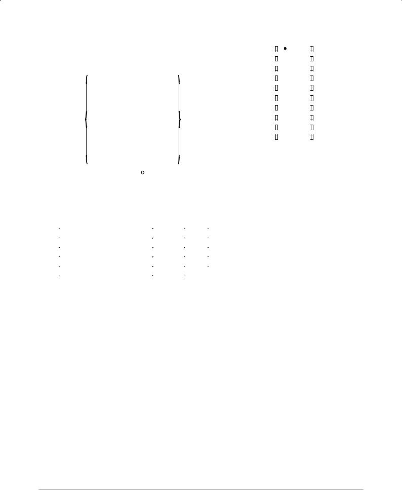
MARKING |
|
|
DIAGRAMS |
|
|
|
20 |
|
|
PDIP±20 |
MC74HC373AN |
|
|
N SUFFIX |
||
|
|
AWLYYWW |
|
20 |
CASE 738 |
|
|
|
|
||
|
|
|
|
1 |
|
1 |
|
|
20 |
||
|
|
||
SOIC WIDE±20 |
|
HC373A |
|
20 |
DW SUFFIX |
|
|
|
AWLYYWW |
||
1 |
CASE 751D |
|
|
|
|
|
|
|
|
1 |
20 |
|
TSSOP±20 |
|
HC |
20 |
DT SUFFIX |
|
373A |
1 |
CASE 948G |
|
ALYW |
|
|
|
1 |
A |
= Assembly Location |
||
WL |
= Wafer Lot |
|
|
YY |
= Year |
|
|
WW = Work Week
ORDERING INFORMATION
Device |
Package |
Shipping |
MC74HC373AN |
PDIP±20 |
1440 / Box |
MC74HC373ADW |
SOIC±WIDE |
38 / Rail |
MC74HC373ADWR2 |
SOIC±WIDE |
1000 / Reel |
MC74HC373ADT |
TSSOP±20 |
75 / Rail |
MC74HC373ADTR2 |
TSSOP±20 |
2500 / Reel |
Semiconductor Components Industries, LLC, 2000 |
1 |
Publication Order Number: |
March, 2000 ± Rev. 8 |
|
MC74HC373A/D |
MC74HC373A
LOGIC DIAGRAM
|
|
D0 |
3 |
|
|
|
2 |
Q0 |
|
|
4 |
|
|
|
5 |
|
|||
|
|
D1 |
|
|
|
Q1 |
|
||
|
7 |
|
|
|
6 |
|
|||
|
|
D2 |
|
|
|
Q2 |
|
||
DATA |
8 |
|
|
|
9 |
|
|||
|
|
|
|
|
|
|
|||
|
D3 |
|
|
|
Q3 |
NONINVERTING |
|||
|
|
|
|
|
|||||
INPUTS |
|
|
13 |
|
|
|
12 |
|
|
|
D4 |
|
|
|
Q4 |
OUTPUTS |
|||
|
|
|
|
|
|||||
|
14 |
|
|
|
15 |
|
|||
|
|
D5 |
|
|
|
Q5 |
|
||
|
17 |
|
|
|
16 |
|
|||
|
|
D6 |
|
|
|
Q6 |
|
||
|
18 |
|
|
|
19 |
|
|||
|
|
D7 |
|
|
|
|
|
||
|
|
|
|
|
Q7 |
|
|||
|
|
|
|
|
|
|
|||
LATCH ENABLE |
11 |
|
|
|
|
PIN 20 = VCC |
|||
|
|
|
|
||||||
1 |
|
|
|
|
PIN 10 = GND |
||||
OUTPUT ENABLE |
|
|
|
|
|||||
|
|
|
|
|
|
||||
|
|
|
|
|
|
|
|||
Design Criteria |
Value |
Units |
|
|
|
Internal Gate Count* |
46.5 |
ea |
|
|
|
Internal Gate Propagation Delay |
1.5 |
ns |
|
|
|
Internal Gate Power Dissipation |
5.0 |
μW |
|
|
|
Speed Power Product |
0.0075 |
pJ |
|
|
|
*Equivalent to a two±input NAND gate. |
|
|
PIN ASSIGNMENT
OUTPUT |
1 |
20 |
VCC |
|
ENABLE |
||||
|
|
|
||
Q0 |
2 |
19 |
Q7 |
|
D0 |
3 |
18 |
D7 |
|
D1 |
4 |
17 |
D6 |
|
Q1 |
5 |
16 |
Q6 |
|
Q2 |
6 |
15 |
Q5 |
|
D2 |
7 |
14 |
D5 |
|
D3 |
8 |
13 |
D4 |
|
Q3 |
9 |
12 |
Q4 |
|
GND |
10 |
11 |
LATCH |
|
|
|
|
ENABLE |
|
|
|
|
FUNCTION TABLE
|
Inputs |
|
Output |
Output |
Latch |
|
|
Enable |
Enable |
D |
Q |
L |
H |
H |
H |
L |
H |
L |
L |
L |
L |
X |
No Change |
H |
X |
X |
Z |
X = Don't Care
Z = High Impedance
http://onsemi.com
2
MC74HC373A
MAXIMUM RATINGS*
Symbol |
Parameter |
|
Value |
Unit |
|
|
|
|
|
VCC |
DC Supply Voltage (Referenced to GND) |
± 0.5 to + 7.0 |
V |
|
Vin |
DC Input Voltage (Referenced to GND) |
± 0.5 to VCC + 0.5 |
V |
|
Vout |
DC Output Voltage (Referenced to GND) |
± 0.5 to VCC + 0.5 |
V |
|
Iin |
DC Input Current, per Pin |
|
± 20 |
mA |
Iout |
DC Output Current, per Pin |
|
± 35 |
mA |
ICC |
DC Supply Current, VCC and GND Pins |
± 75 |
mA |
|
PD |
Power Dissipation in Still Air, |
Plastic DIP² |
750 |
mW |
|
|
SOIC Package² |
500 |
|
|
|
TSSOP Package² |
450 |
|
|
|
|
|
|
Tstg |
Storage Temperature |
|
± 65 to + 150 |
_C |
TL |
Lead Temperature, 1 mm from Case for 10 Seconds |
|
_C |
|
|
(Plastic DIP, SOIC, SSOP or TSSOP Package) |
260 |
|
|
|
|
|
|
|
This device contains protection circuitry to guard against damage due to high static voltages or electric fields. However, precautions must be taken to avoid applications of any voltage higher than maximum rated voltages to this high±impedance circuit. For proper operation, Vin and Vout should be constrained to the
range GND v (Vin or Vout) v VCC. Unused inputs must always be
tied to an appropriate logic voltage level (e.g., either GND or VCC). Unused outputs must be left open.
*Maximum Ratings are those values beyond which damage to the device may occur. Functional operation should be restricted to the Recommended Operating Conditions.
²Derating Ð Plastic DIP: ± 10 mW/ _C from 65_ to 125_C SOIC Package: ± 7 mW/_C from 65_ to 125_C
TSSOP Package: ± 6.1 mW/_C from 65_ to 125_C
For high frequency or heavy load considerations, see Chapter 2 of the ON Semiconductor High±Speed CMOS Data Book (DL129/D).
RECOMMENDED OPERATING CONDITIONS
Symbol |
Parameter |
|
Min |
Max |
Unit |
|
|
|
|
|
|
VCC |
DC Supply Voltage (Referenced to GND) |
|
2.0 |
6.0 |
V |
Vin, Vout |
DC Input Voltage, Output Voltage (Referenced to GND) |
0 |
VCC |
V |
|
TA |
Operating Temperature, All Package Types |
|
± 55 |
+ 125 |
_C |
tr, tf |
Input Rise and Fall Time |
VCC = 2.0 V |
0 |
1000 |
ns |
|
(Figure 1) |
VCC = 4.5 V |
0 |
500 |
|
|
|
VCC = 6.0 V |
0 |
400 |
|
DC ELECTRICAL CHARACTERISTICS (Voltages Referenced to GND)
|
|
|
|
|
Guaranteed Limit |
|
||
|
|
|
|
|
|
|
|
|
|
|
|
|
VCC |
± 55 to |
|
|
|
Symbol |
Parameter |
Test Conditions |
V |
25_C |
v 85_C |
v 125_C |
Unit |
|
|
|
|
|
|
|
|
|
|
VIH |
Minimum High±Level Input |
Vout = VCC ± 0.1 V |
2.0 |
1.5 |
1.5 |
1.5 |
V |
|
|
Voltage |
|Iout| v 20 |
μA |
3.0 |
2.1 |
2.1 |
2.1 |
|
|
|
|
|
4.5 |
3.15 |
3.15 |
3.15 |
|
|
|
|
|
6.0 |
4.2 |
4.2 |
4.2 |
|
|
|
|
|
|
|
|
|
|
VIL |
Maximum Low±Level Input |
Vout = 0.1 V |
2.0 |
0.5 |
0.5 |
0.5 |
V |
|
|
Voltage |
|Iout| v 20 μA |
3.0 |
0.9 |
0.9 |
0.9 |
|
|
|
|
|
|
4.5 |
1.35 |
1.35 |
1.35 |
|
|
|
|
|
6.0 |
1.8 |
1.8 |
1.8 |
|
|
|
|
|
|
|
|
|
|
VOH |
Minimum High±Level Output |
Vin = VIH |
μA |
2.0 |
1.9 |
1.9 |
1.9 |
V |
|
Voltage |
|Iout| v 20 |
4.5 |
4.4 |
4.4 |
4.4 |
|
|
|
|
|
|
6.0 |
5.9 |
5.9 |
5.9 |
|
|
|
|
|
|
|
|
|
|
|
|
Vin = VIH |
|Iout| v 2.4 mA |
3.0 |
2.48 |
2.34 |
2.2 |
|
|
|
|
|Iout| v 6.0 mA |
4.5 |
3.98 |
3.84 |
3.7 |
|
|
|
|
|Iout| v 7.8 mA |
6.0 |
5.48 |
5.34 |
5.2 |
|
VOL |
Maximum Low±Level Output |
Vin = VIL |
μA |
2.0 |
0.1 |
0.1 |
0.1 |
V |
|
Voltage |
|Iout| v 20 |
4.5 |
0.1 |
0.1 |
0.1 |
|
|
|
|
|
|
6.0 |
0.1 |
0.1 |
0.1 |
|
|
|
|
|
|
|
|
|
|
|
|
Vin = VIL |
|Iout| v 2.4 mA |
3.0 |
0.26 |
0.33 |
0.4 |
|
|
|
|
|Iout| v 6.0 mA |
4.5 |
0.26 |
0.33 |
0.4 |
|
|
|
|
|Iout| v 7.8 mA |
6.0 |
0.26 |
0.33 |
0.4 |
|
http://onsemi.com
3
 Loading...