


MC74HC541AN
MOTOROLA MC74HC541AN, MC74HC541AFEL, MC74HC541AFL1, MC74HC541AFR1, MC74HC541AFR2 Datasheet
...
Semiconductor Components Industries, LLC, 2000
March, 2000 – Rev. 2
1 Publication Order Number:
MC74HC541A/D
MC74HC541A
Octal 3-State Non-Inverting
Buffer/Line Driver/
Line Receiver
High–Performance Silicon–Gate CMOS
The MC74HC541A is identical in pinout to the LS541. The device
inputs are compatible with Standard CMOS outputs. External pullup
resistors make them compatible with LSTTL outputs.
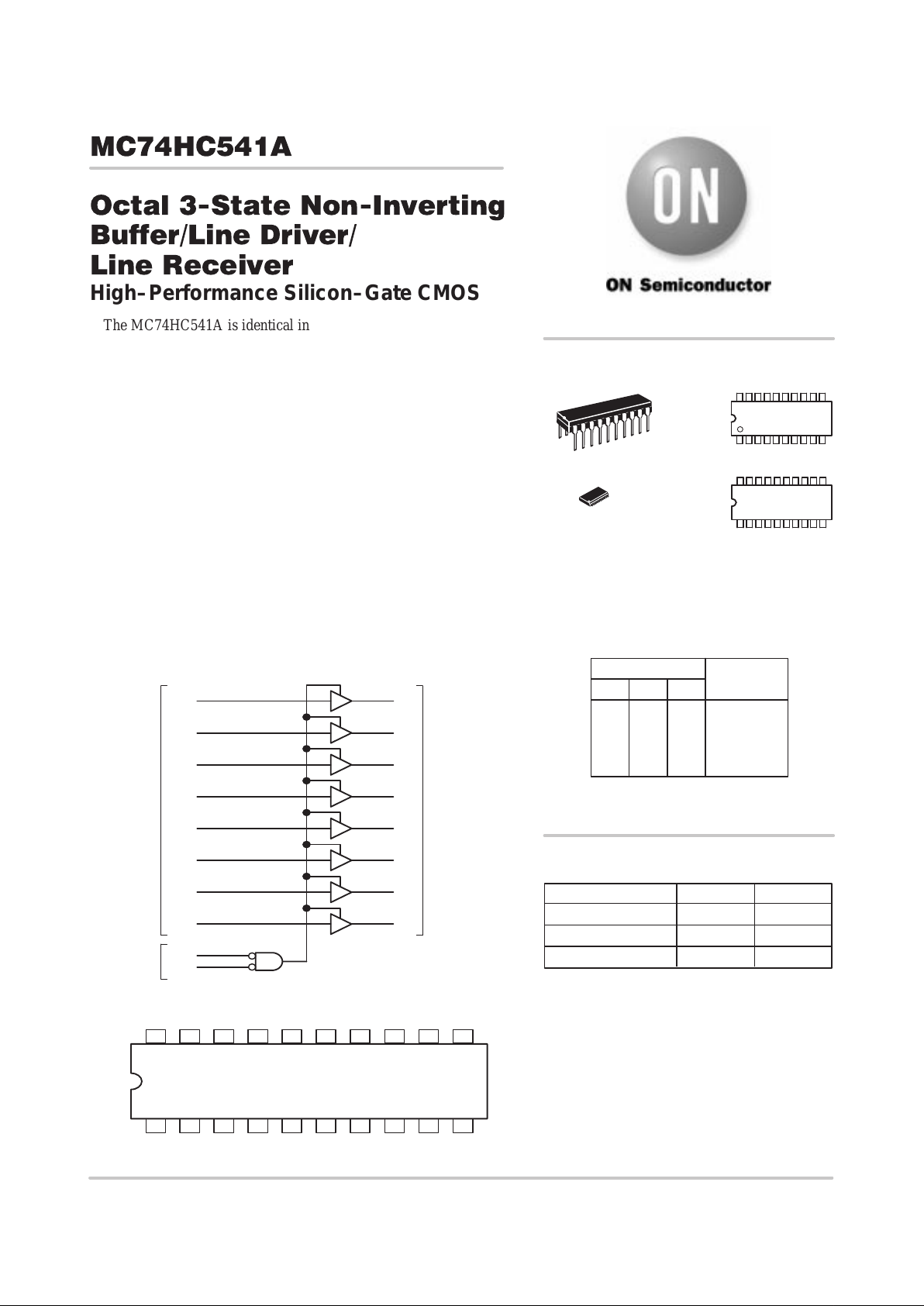
The HC541A is an octal non–inverting buffer/line driver/line
receiver designed to be used with 3–state memory address drivers,
clock drivers, and other bus–oriented systems. This device features
inputs and outputs on opposite sides of the package and two ANDed
active–low output enables.
The HC541A is similar in function to the HC540A, which has
inverting outputs.
• Output Drive Capability: 15 LSTTL Loads
• Outputs Directly Interface to CMOS, NMOS and TTL
• Operating Voltage Range: 2 to 6V
• Low Input Current: 1µA
• High Noise Immunity Characteristic of CMOS Devices
• In Compliance With the JEDEC Standard No. 7A Requirements
• Chip Complexity: 134 FETs or 33.5 Equivalent Gates
18
Y1
2
A1
17
Y2
3
A2
16
Y3
4
A3
15
Y4
5
A4
14
Y5
6
A5
13
Y6
7
A6
12
Y7
8
A7
11
Y8
9
A8
OE1
OE2
1
19
Output
Enables
Data
Inputs
Non–Inverting
Outputs
PIN 20 = V
CC
PIN 10 = GND
LOGIC DIAGRAM
Pinout: 20–Lead Packages (Top View)
1920 18 17 16 15 14
21 34567
V
CC
13
8
12
9
11
10
OE2 Y1 Y2 Y3 Y4 Y5 Y6 Y7 Y8
OE1 A1 A2 A3 A4 A5 A6 A7 A8 GND
http://onsemi.com
MARKING
DIAGRAMS
1
20
A = Assembly Location
WL = Wafer Lot
YY = Year
WW = Work Week
SOIC WIDE–20
DW SUFFIX
CASE 751D
HC541A
AWLYYWW
PDIP–20
N SUFFIX
CASE 738
1
20
MC74HC541AN
AWLYYWW
1
20
1
20
Device Package Shipping
ORDERING INFORMATION
MC74HC541AN PDIP–20 1440 / Box
MC74HC541ADW SOIC–WIDE
38 / Rail
MC74HC541ADWR2 SOIC–WIDE 1000 / Reel
L
L
H
X
L
L
X
H
L
H
X
X
FUNCTION TABLE
Inputs
Output Y
OE1 OE2 A
L
H
Z
Z
Z = High Impedance
X = Don’t Care
MC74HC541A
http://onsemi.com
2
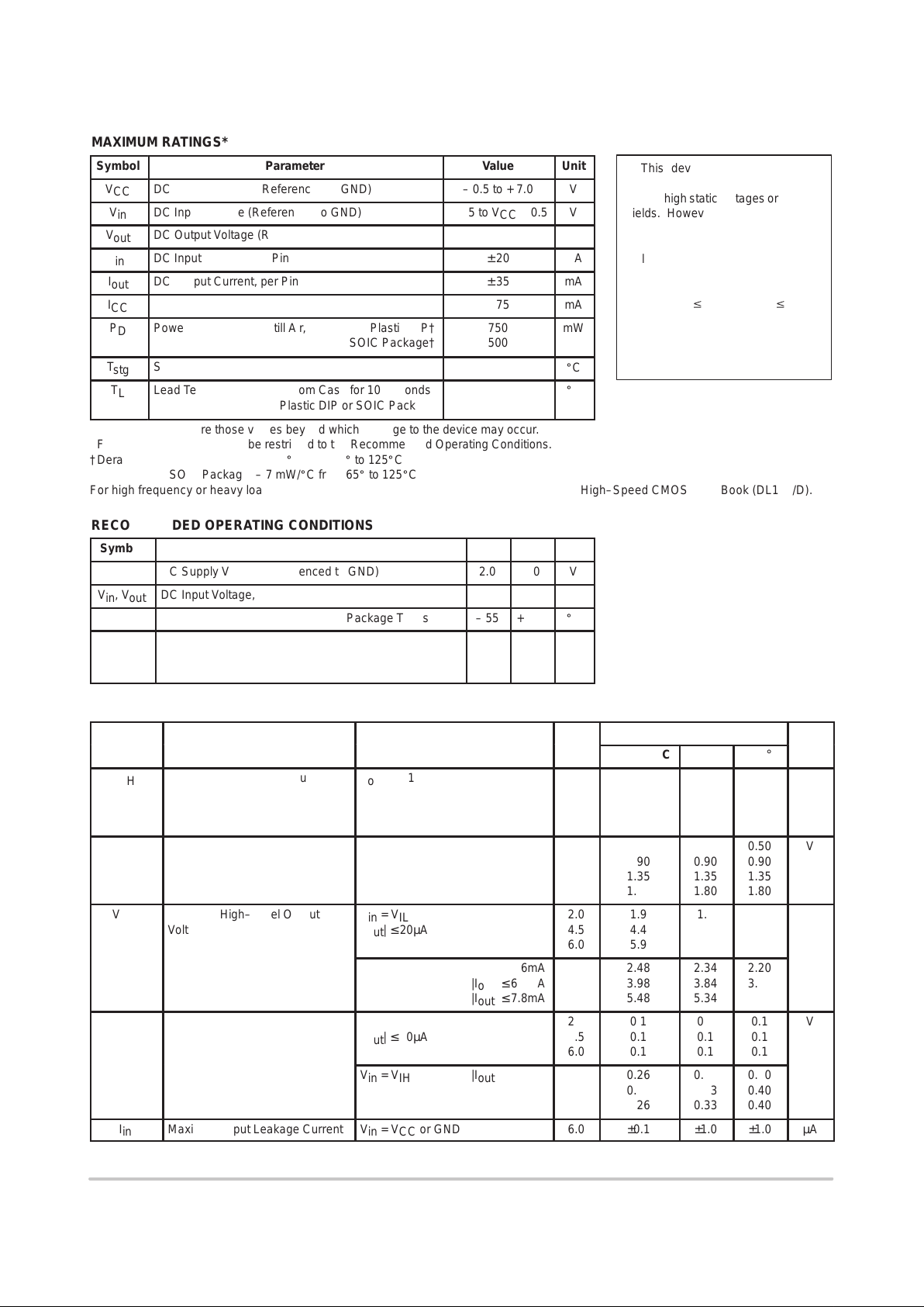
MAXIMUM RATINGS*
Symbol
Parameter
Value
Unit
V
CC
DC Supply Voltage (Referenced to GND)
– 0.5 to + 7.0
V
V
in
DC Input Voltage (Referenced to GND)
– 0.5 to VCC + 0.5
V
V
out
DC Output Voltage (Referenced to GND)
– 0.5 to VCC + 0.5
V
I
in
DC Input Current, per Pin
± 20
mA
I
out
DC Output Current, per Pin
± 35
mA
I
CC
DC Supply Current, VCC and GND Pins
± 75
mA
ÎÎ
Î
P
D
ОООООООООООО
Î
Power Dissipation in Still Air, Plastic DIP†
SOIC Package†
ÎÎÎ
Î
750
500
Î
Î
mW
T
stg
Storage Temperature Range
– 65 to + 150
_
C
T
L
Lead Temperature, 1 mm from Case for 10 Seconds
Plastic DIP or SOIC Package
260
_
C
*Maximum Ratings are those values beyond which damage to the device may occur.
Functional operation should be restricted to the Recommended Operating Conditions.
†Derating — Plastic DIP: – 10 mW/_C from 65_ to 125_C
SOIC Package: – 7 mW/_C from 65_ to 125_C
For high frequency or heavy load considerations, see Chapter 2 of the ON Semiconductor High–Speed CMOS Data Book (DL129/D).
RECOMMENDED OPERATING CONDITIONS
Symbol
Parameter
Min
ÎÎ
Max
Unit
V
CC
DC Supply Voltage (Referenced to GND)
2.0
ÎÎ
6.0
V
Vin, V
out
DC Input Voltage, Output Voltage (Referenced to GND)
0
ÎÎ
V
CC
V
T
A
Operating Temperature Range, All Package Types
– 55
ÎÎ
+ 125
_
C
ÎÎ
Î
ÎÎ
Î
tr, t
f
ООООООООООООО
Î
ООООООООООООО
Î
Input Rise/Fall Time VCC = 2.0 V
(Figure 1) VCC = 4.5 V
VCC = 6.0 V
Î
Î
Î
Î
0
0
0
ÎÎ
ÎÎ
ÎÎ
1000
500
400
Î
Î
Î
Î
ns
DC CHARACTERISTICS (Voltages Referenced to GND)
V
Guaranteed Limit
Symbol Parameter Condition
V
CC
V
–55 to 25°C ≤85°C ≤125°C Unit
V
IH
Minimum High–Level Input
Voltage
V
out
= 0.1V
|I
out
| ≤ 20µA
2.0
3.0
4.5
6.0
1.50
2.10
3.15
4.20
1.50
2.10
3.15
4.20
1.50
2.10
3.15
4.20
V
V
IL
Maximum Low–Level Input
Voltage
V
out
= VCC – 0.1V
|I
out
| ≤ 20µA
2.0
3.0
4.5
6.0
0.50
0.90
1.35
1.80
0.50
0.90
1.35
1.80
0.50
0.90
1.35
1.80
V
V
OH
Minimum High–Level Output
Voltage
Vin = V
IL
|I
out
| ≤ 20µA
2.0
4.5
6.0
1.9
4.4
5.9
1.9
4.4
5.9
1.9
4.4
5.9
V
Vin = V
IL
|I
out
| ≤ 3.6mA
|I
out
| ≤ 6.0mA
|I
out
| ≤ 7.8mA
3.0
4.5
6.0
2.48
3.98
5.48
2.34
3.84
5.34
2.20
3.70
5.20
V
OL
Maximum Low–Level Output
Voltage
Vin = V
IH
|I
out
| ≤ 20µA
2.0
4.5
6.0
0.1
0.1
0.1
0.1
0.1
0.1
0.1
0.1
0.1
V
Vin = V
IH
|I
out
| ≤ 3.6mA
|I
out
| ≤ 6.0mA
|I
out
| ≤ 7.8mA
3.0
4.5
6.0
0.26
0.26
0.26
0.33
0.33
0.33
0.40
0.40
0.40
I
in
Maximum Input Leakage Current Vin = VCC or GND 6.0 ±0.1 ±1.0 ±1.0 µA
This device contains protection
circuitry to guard against damage
due to high static voltages or electric
fields. However, precautions must
be taken to avoid applications of any
voltage higher than maximum rated
voltages to this high–impedance circuit. For proper operation, Vin and
V
out
should be constrained to the
range GND v (Vin or V
out
) v VCC.
Unused inputs must always be
tied to an appropriate logic voltage
level (e.g., either GND or VCC).
Unused outputs must be left open.
MC74HC541A
http://onsemi.com
3
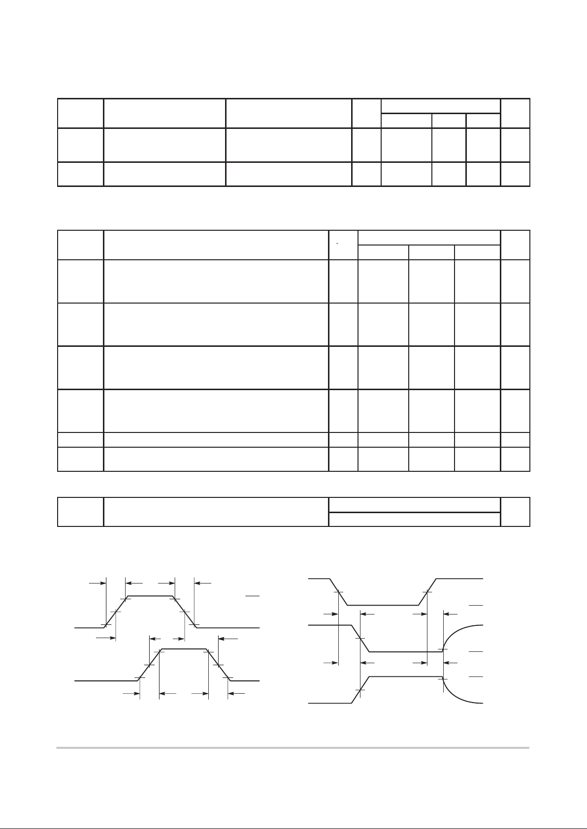
DC CHARACTERISTICS (Voltages Referenced to GND)
Guaranteed Limit
V
CC
V
Symbol Unit≤125°C≤85°C–55 to 25°C
V
CC
V
ConditionParameter
I
OZ
Maximum Three–State Leakage
Current
Output in High Impedance State
Vin = VIL or V
IH
V
out
= VCC or GND
6.0 ±0.5 ±5.0 ±10.0 µA
I
CC
Maximum Quiescent Supply
Current (per Package)
Vin = VCC or GND
I
out
= 0µA
6.0 4 40 160 µA
NOTE: Information on typical parametric values can be found in Chapter 2 of the ON Semiconductor High–Speed CMOS Data Book
(DL129/D).
AC CHARACTERISTICS (C
L
= 50 pF, Input tr = tf = 6 ns)
V
Guaranteed Limit
Symbol Parameter
V
CC
V
–55 to 25°C ≤85°C ≤125°C Unit
t
PLH
,
t
PHL
Maximum Propagation Delay, Input A to Output Y
(Figures 1 and 3)
2.0
3.0
4.5
6.0
80
30
18
15
100
40
23
20
120
55
28
25
ns
t
PLZ
,
t
PHZ
Maximum Propagation Delay, Output Enable to Output Y
(Figures 2 and 4)
2.0
3.0
4.5
6.0
110
45
25
21
140
60
31
26
165
75
38
31
ns
t
PZL
,
t
PZH
Maximum Propagation Delay, Output Enable to Output Y
(Figures 2 and 4)
2.0
3.0
4.5
6.0
110
45
25
21
140
60
31
26
165
75
38
31
ns
t
TLH
,
t
THL
Maximum Output Transition Time, Any Output
(Figures 1 and 3)
2.0
3.0
4.5
6.0
60
22
12
10
75
28
15
13
90
34
18
15
ns
C
in
Maximum Input Capacitance 10 10 10 pF
C
out
Maximum Three–State Output Capacitance (Output in High
Impedance State)
15 15 15 pF
NOTE: For propagation delays with loads other than 50 pF, and information on typical parametric values, see Chapter 2 of the ON
Semiconductor High–Speed CMOS Data Book (DL129/D).
Typical @ 25°C, VCC = 5.0 V, VEE = 0 V
C
PD
Power Dissipation Capacitance (Per Buffer)*
35
pF
*Used to determine the no–load dynamic power consumption: PD = CPD V
CC
2
f + ICC VCC. For load considerations, see Chapter 2 of the
ON Semiconductor High–Speed CMOS Data Book (DL129/D).
Figure 1.
V
CC
GND
INPUT A
OUTPUT Y
t
PLH
OE1 or OE2
50%
V
CC
GND
OUTPUT Y
t
PZL
OUTPUT Y
t
PZH
HIGH
IMPEDANCE
V
OL
V
OH
HIGH
IMPEDANCE
10%
90%
t
PLZ
t
PHZ
50%
50%
t
PHL
90%
50%
10%
t
r
t
TLH
t
f
t
THL
Figure 2.
SWITCHING WAVEFORMS
90%
50%
10%
50%
 Loading...