


Motorola MC74ACT652DWR2, MC74ACT652N, MC74ACT652DW, MC74AC652N, MC74AC652DW Datasheet
...
Octal Transceiver/Register With
3$State Outputs (Non$Inverting)
The MC74AC/ACT652 consists of registered bus transceiver circuits, with outputs, D-type flip-flops and control circuitry providing multiplexed transmission of data directly from the input bus or from the internal storage registers. Data on the A or B bus will be loaded into the respective registers on the LOW-to-HIGH transition of the appropriate clock pin (CAB or CBA). The four fundamental data handling functions available are illustrated in Figures 1 to 4.
•Independent Registers for A and B Buses
•Multiplexed Real-Time and Stored Data Transfers
•Choice of True and Inverting Data Paths
•3-State Outputs
•300 mil Slim Dual-in-Line Package
•Outputs Source/Sink 24 mA
•′ACT652 Has TTL Compatible Inputs
REAL TIME TRANSFER
A-BUS TO B-BUS
|
A-BUS |
REG |
REG |
|
B-BUS |
REAL TIME TRANSFER
B-BUS TO A-BUS
|
A-BUS |
REG |
REG |
|
B-BUS |
|
Figure 1 |
|
Figure 2 |
|
STORAGE |
|
TRANSFER |
FROM BUS TO REGISTER |
FROM REGISTER TO BUS |
||
|
A-BUS |
|
A-BUS |
REG |
REG |
REG |
REG |
|
B-BUS |
|
B-BUS |
|
Figure 3 |
|
Figure 4 |
MC74AC652
MC74ACT652
OCTAL TRANSCEIVER/ REGISTER WITH 3-STATE OUTPUTS (NON-INVERTING)
24
1
N SUFFIX
CASE 724-03
PLASTIC PACKAGE
24


1
DW SUFFIX
CASE 751E-04
SOIC PACKAGE
PIN NAMES
A0 ± A7 |
Data Register A Inputs |
||
|
|
|
Data Register A Outputs |
B0 ± B7 |
Data Register B Inputs |
||
CAB, CBA |
Data Register B Outputs |
||
Clock Pulse Inputs |
|||
SAB, |
SBA |
|
Transmit/Receive Inputs |
GAB, GBA |
Output Enable Inputs |
||
MAXIMUM RATINGS*
Symbol |
Parameter |
Value |
Unit |
|
|
|
|
VCC |
DC Supply Voltage (Referenced to GND) |
±0.5 to +7.0 |
V |
Vin |
DC Input Voltage (Referenced to GND) |
±0.5 to VCC + 0.5 |
V |
Vout |
DC Output Voltage (Referenced to GND) |
±0.5 to VCC + 0.5 |
V |
Iin |
DC Input Current, per Pin |
± 20 |
mA |
Iout |
DC Output Sink/Source Current, per Pin |
± 50 |
mA |
ICC |
DC VCC or GND Current per Output Pin |
± 50 |
mA |
Tstg |
Storage Temperature |
±65 to +150 |
°C |
*Maximum Ratings are those values beyond which damage to the device may occur. Functional operation should be restricted to the Recommended Operating Conditions.
FACT DATA
5-1
MC74AC652 MC74ACT652
Pinout: 24-Lead Plastic Package (Top View)
VCC |
CBA |
|
SBA |
GBA |
B0 |
|
B1 |
|
B2 |
|
B3 |
|
B4 |
|
B5 |
|
B6 |
|
B7 |
|||||
|
24 |
|
23 |
|
22 |
|
21 |
|
20 |
|
19 |
|
18 |
|
17 |
|
16 |
|
15 |
|
14 |
|
13 |
|
|
|
|
|
|
|
|
|
|
|
|
|
|
|
|
|
|
|
|
|
|
|
|
|
|
|
|
|
|
|
|
|
|
|
|
|
|
|
|
|
|
|
|
|
|
|
|
|
|
|
|
1 |
|
2 |
|
3 |
|
4 |
|
5 |
|
6 |
|
7 |
|
8 |
|
9 |
|
10 |
|
11 |
|
12 |
|
|
CAB |
SAB |
GAB |
A0 |
|
A1 |
|
A2 |
A3 |
|
A4 |
|
A5 |
|
A6 |
|
A7 |
GND |
||||||
LOGIC SYMBOL
|
|
|
|
|
|
|
|
|
|
|
|
|
|
|
|
|
|
|
|
CAB |
B0 |
B1 |
B2 |
B3 |
B4 |
B5 |
B6 |
B7 |
|||||||||
|
SAB |
|
|
|
|
|
|
|
|
|
|
|
|
|
|
|
|
|
|
GAB |
|
|
|
|
|
|
|
|
|
|
|
|
|
|
|
|
|
|
CBA |
|
|
|
|
|
|
|
|
|
|
|
|
|
|
|
|
|
|
SBA |
|
|
|
|
|
|
|
|
|
|
|
|
|
|
|
|
|
|
GBA |
A0 |
A1 |
A2 |
A3 |
A4 |
A5 |
A6 |
A7 |
|||||||||
|
|
|
||||||||||||||||
|
|
|
|
|
|
|
|
|
|
|
|
|
|
|
|
|
|
|
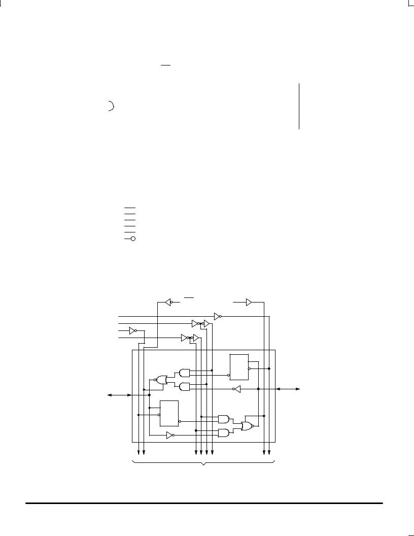
LOGIC DIAGRAM |
|
GBA |
GAB |
CBA |
|
SBA |
|
CAB |
|
SAB |
|
1 OF 8 CHANNELS |
D0 |
|
|
|
C0 |
A0 |
B0 |
|
|
D0 |
|
C0 |
|
TO 7 OTHER CHANNELS
Please note that this diagram is provided only for the understanding of logic operations and should not be used to estimate propagation delays.
FACT DATA
5-2

MC74AC652 MC74ACT652
FUNCTION TABLE
|
|
|
|
Inputs |
|
|
|
Data I/O* |
Operation or Function |
||
|
|
|
|
|
|
|
|
|
|
|
|
GAB |
GBA |
|
CAB |
CBA |
SAB |
SBA |
|
A0 ± A7 |
B0 ± B7 |
||
|
|
|
|||||||||
L |
|
H |
|
H or L |
H or L |
X |
X |
|
Input |
Input |
Isolation |
L |
|
H |
|
|
|
X |
X |
|
Store A and B Data |
||
|
|
|
|
|
|||||||
|
|
|
|
|
|
|
|
|
|
|
|
X |
|
H |
|
|
H or L |
X |
X |
|
Input |
Unspecified* |
Store A, Hold B |
H |
|
H |
|
|
|
X** |
X |
|
Input |
Output |
Store A in Both Registers |
|
|
|
|
|
|
|
|
|
|
|
|
L |
|
X |
|
H or L |
|
X |
X |
Unspecified* |
Input |
Hold A, Store B |
|
L |
|
L |
|
|
|
X |
X** |
|
Output |
Input |
Store B in Both Registers |
|
|
|
|
|
|
|
|
|
|
|
|
L |
|
L |
|
X |
X |
X |
L |
|
Output |
Input |
Real-Time B Data to A Bus |
L |
|
L |
|
X |
H or L |
X |
H |
|
Stored B Data to A Bus |
||
|
|
|
|
|
|||||||
|
|
|
|
|
|
|
|
|
|
|
|
H |
|
H |
|
X |
X |
L |
X |
|
Input |
Output |
Real-Time A Data to B Bus |
H |
|
H |
|
H or L |
X |
H |
X |
|
Stored A Data to B Bus |
||
|
|
|
|
|
|||||||
|
|
|
|
|
|
|
|
|
|
|
|
H |
|
L |
|
H or L |
H or L |
H |
H |
|
Output |
Output |
Stored A Data to B Bus and |
|
|
|
Stored B Data to A Bus |
||||||||
|
|
|
|
|
|
|
|
|
|
|
|
|
|
|
|
|
|
|
|
|
|
|
|
*The data output functions may be enabled or disabled by various signals at the GBA and GAB inputs. Data input functions are always enabled; i.e., data at the bus pins will be stored on every LOW-to-HIGH transition of the appropriate clock inputs.
**Select control = L: clocks can occur simultaneously.
H = HIGH Voltage Level; L = LOW Voltage Level; X = Immaterial; = LOW-to-HIGH Transition
RECOMMENDED OPERATING CONDITIONS
Symbol |
Parameter |
|
Min |
Typ |
Min |
Unit |
|
|
|
|
|
|
|
|
|
VCC |
Supply Voltage |
′AC |
2.0 |
5.0 |
6.0 |
V |
|
|
|
|
|
||||
′ACT |
4.5 |
5.0 |
5.5 |
||||
|
|
|
|||||
|
|
|
|
|
|
|
|
Vin, Vout |
DC Input Voltage, Output Voltage (Ref. to GND) |
|
0 |
|
VCC |
V |
|
|
Input Rise and Fall Time (Note 1) |
VCC @ 3.0 V |
|
150 |
|
|
|
tr, tf |
VCC @ 4.5 V |
|
40 |
|
ns/V |
||
′AC Devices except Schmitt Inputs |
|
|
|||||
|
|
VCC @ 5.5 V |
|
25 |
|
|
|
tr, tf |
Input Rise and Fall Time (Note 2) |
VCC @ 4.5 V |
|
10 |
|
ns/V |
|
′ACT Devices except Schmitt Inputs |
VCC @ 5.5 V |
|
8.0 |
|
|||
|
|
|
|
|
|||
TJ |
Junction Temperature (PDIP) |
|
|
|
140 |
°C |
|
TA |
Operating Ambient Temperature Range |
|
±40 |
25 |
85 |
°C |
|
IOH |
Output Current Ð HIGH |
|
|
|
±24 |
mA |
|
IOL |
Output Current Ð LOW |
|
|
|
24 |
mA |
1.Vin from 30% to 70% VCC; see individual Data Sheets for devices that differ from the typical input rise and fall times.
2.Vin from 0.8 V to 2.0 V; see individual Data Sheets for devices that differ from the typical input rise and fall times.
FACT DATA
5-3
 Loading...