


Integrated Device Technology Inc IDT70121L25J, IDT70121L35J, IDT70121L45J, IDT70121L55J, IDT70121S25J Datasheet
...
|
|
|
|
|
|
|
|
|
HIGH-SPEED |
IDT70121S/L |
|
|
|
|
|
|
|
|
|
2K x 9 DUAL-PORT |
IDT70125S/L |
|
|
|
|
|
|
|
|
|
||
|
|
|
|
|
|
|
|
|
||
|
|
|
|
|
|
|
|
|
STATIC RAM WITH BUSY & INTERRUPT |
|
Integrated Device Technology, Inc. |
|
|
|
|||||||
|
|
|
|
|
|
|
|
|
|
|
|
|
|
|
|
|
|
|
|
|
|
FEATURES:
•High-speed access
–Commercial: 25/35/45/55ns (max.)
•Low-power operation
–IDT70121/70125S Active: 500mW (typ.) Standby: 5mW (typ.)
–IDT70121/70125L Active: 500mW (typ.) Standby: 1mW (typ.)
•Fully asychronous operation from either port
•MASTER IDT70121 easily expands data bus width to 18 bits or more using SLAVE IDT70125 chip
•On-chip port arbitration logic (IDT70121 only)
•BUSY output flag on Master; BUSY input on Slave
•INT flag for port-to-port communication
•Battery backup operation—2V data retention
•TTL-compatible, signal 5V (±10%) power supply
•Available in 52-pin PLCC
•Industrial temperature range (–40°C to +85°C) is available, tested to military electrical specifications
DESCRIPTION:
The IDT70121/IDT70125 are high-speed 2K x 9 Dual-Port Static RAMs. The IDT70121 is designed to be used as a stand-alone 9-bit Dual-Port RAM or as a “MASTER” Dual-Port RAM together with the IDT70125 “SLAVE” Dual-Port in 18- bit-or-more word width systems. Using the IDT MASTER/ SLAVE Dual-Port RAM approach in 18-bit-or-wider memory system applications results in full-speed, error-free operation without the need for additional discrete logic.
Both devices provide two independent ports with separate control, address, and I/O pins that permit independent, asynchronous access for reads or writes to any location in memory. An automatic power-down feature, controlled by CE, permits the on-chip circuitry of each port to enter a very low standby power mode.
The IDT70121/IDT70125 utilizes a 9-bit wide data path to allow for Data/Control and parity bits at the user’s option. This feature is especially useful in data communications applications where it is necessary to use a parity bit for transmission/reception error checking.
FUNCTIONAL BLOCK DIAGRAM
OEL |
OER |
CEL |
CER |
W |
R/WR |
R/ L |
|
I/O0L- I/O8L |
|
|
I/O |
|
|
I/O |
|
|
I/O0R-I/O8R |
|
|
|
|
|
|
|
|
|
|||
|
|
|
Control |
|
Control |
|
|
|
||
(1,2) |
|
|
|
|
|
|
|
|
|
(1,2) |
|
|
|
|
|
|
|
|
|
||
BUSYL |
|
|
|
|
|
|
|
|
|
BUSYR |
A10L |
|
|
|
|
|
|
|
|
|
A11R |
Address |
|
|
MEMORY |
|
|
|
Address |
|||
|
|
|
|
|
|
|
||||
A0L |
Decoder |
|
|
ARRAY |
|
|
|
Decoder |
A0R |
|
|
|
|
|
|
|
|
|
|
||
NOTES:
1.70121 (MASTER): BUSY is non-tri- stated push-pull output.
70125 (SLAVE): BUSY is input.
2.INT is totem-pole output.
(2)
INTL
|
11 |
11 |
|
|
|
||
|
ARBITRATION |
|
|
CEL |
INTERRUPT |
CER |
|
OEL |
SEMAPHORE |
OER |
|
LOGIC |
|||
R/WL |
R/WR |
||
|
(2)
INTR
2654 drw 01
The IDT logo is a registered trademark of Integrated Device Technology, Inc.
COMMERCIAL TEMPERATURE RANGE |
OCTOBER 1996 |
|
©1996 Integrated Device Technology, Inc. |
For latest information contact IDT’s web site at www.idt.com or fax-on-demand at 408-492-8391. |
DSC-2654/4 |
6.10 |
1 |
IDT 70121/70125S/L |
|
HIGH-SPEED 2K x 9 DUAL-PORT STATIC RAM WITH BUSY & INTERRUPT |
COMMERCIAL TEMPERATURE RANGE |
DESCRIPTION (Cont'd):
Fabricated using IDT’s CMOS high-performance technology, these devices typically operate on only 500mW of power. Low-power (L) versions offer battery backup data
retention capability with each port typically consuming 200μW from a 2V battery.
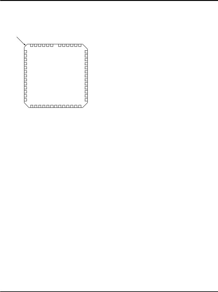
The IDT70121/IDT70125 devices are packaged in a 52-pin PLCC.
PIN CONFIGURATIONS (1,2)
NDEX |
|
|
A0L |
LOE |
A10L |
INTL BUSY L R/WL LCE |
VCC CER R/WR BUSYR RINT |
A10R |
|
||||||||
|
|
A1L |
7 |
6 |
5 |
4 |
3 |
2 |
|
|
52 |
51 |
50 |
49 |
48 |
47 |
|
|
|
8 |
|
|
|
|
|
|
|
|
|
|
|
|
46 |
OE |
|
|
|
|
|
|
|
|
1 |
|
|
|
|
|
|
||||
|
|
|
|
|
|
|
|
|
|
|
|
|
|
|
R |
||
|
|
A2L |
9 |
|
|
|
|
|
|
|
|
|
|
|
|
45 |
A0R |
|
|
A3L |
10 |
|
|
|
|
|
|
|
|
|
|
|
|
44 |
A1R |
|
|
A4L |
11 |
|
|
|
IDT70121/125 |
|
|
43 |
A2R |
||||||
|
|
A5L |
12 |
|
|
|
|
|
42 |
A3R |
|||||||
|
|
|
|
|
|
J52-1 |
|
|
|
|
|||||||
|
|
A6L |
13 |
|
|
|
|
|
|
|
|
41 |
A4R |
||||
|
|
|
|
|
|
|
|
|
|
|
|
|
|
||||
|
|
A7L |
14 |
|
|
|
|
PLCC |
|
|
|
|
40 |
A5R |
|||
|
|
A8L |
15 |
|
|
|
|
|
|
|
|
39 |
A6R |
||||
|
|
|
|
|
TOP VIEW(3) |
|
|
|
|||||||||
|
|
A9L |
16 |
|
|
|
|
|
|
|
|
|
|
|
|
38 |
A7R |
|
I/O0L |
17 |
|
|
|
|
|
|
|
|
|
|
|
|
37 |
A8R |
|
|
I/O1L |
18 |
|
|
|
|
|
|
|
|
|
|
|
|
36 |
A9R |
|
|
I/O2L |
19 |
|
|
|
|
|
|
|
|
|
|
|
|
35 |
I/O8R |
|
|
I/O3L |
20 |
|
|
|
|
|
|
|
|
|
|
|
|
34 |
I/O7R |
|
|
|
|
21 |
22 |
23 |
24 |
25 |
26 |
27 |
|
28 |
29 |
30 |
31 |
32 |
33 |
|
|
|
|
I/O4L |
I/O5L |
I/O6L |
I/O7L |
I/O8L |
GND |
I/O0R |
I/O1R |
I/O2R |
I/O3R |
I/O4R |
I/O5R |
I/O6R |
2654 drw 02 |
|
NOTES:
1.All Vcc pins must be connected to the power supply.
2.All GND pins must be connected to the ground supply.
3.This text does not indicate the orientation of the actual part-marking.
RECOMMENDED OPERATING TEMPERATURE AND SUPPLY VOLTAGE
Grade |
Ambient Temperature |
GND |
VCC |
Commercial |
0°C to +70°C |
0V |
5.0V ± 10% |
|
|
|
|
|
|
|
2654 tbl 02 |
RECOMMENDED DC
OPERATING CONDITIONS
Symbol |
Parameter |
Min. |
Typ. |
Max. |
Unit |
|
|
|
|
|
|
VCC |
Supply Voltage |
4.5 |
5 |
5.5 |
V |
|
|
|
|
|
|
GND |
Supply Voltage |
0 |
0 |
0.0 |
V |
|
|
|
|
|
|
VIH |
Input High Voltage |
2.2 |
– |
6.0(2) |
V |
VIL |
Input Low Voltage |
–0.5(1) |
– |
0.8 |
V |
NOTES: |
|
|
|
|
2654 tbl 03 |
1.VIL > -1.5V for pulse width less than 10ns.
2.VTERM must not exceed Vcc + 0.5V.
ABSOLUTE MAXIMUM RATINGS(1)
Symbol |
Rating |
Commercial |
Unit |
|
|
|
|
VTERM(2) |
Terminal Voltage |
–0.5 to +7.0 |
V |
|
with Respect to GND |
|
|
TA |
Operating |
0 to +70 |
°C |
|
Temperature |
|
|
TBIAS |
Temperature |
–55 to +125 |
°C |
|
Under Bias |
|
|
TSTG |
Storage |
–55 to +125 |
°C |
|
Temperature |
|
|
IOUT |
DC Output |
50 |
mA |
|
Current |
|
|
NOTES: |
|
|
2654 tbl 01 |
1.Stresses greater than those listed under ABSOLUTE MAXIMUM RATINGS may cause permanent damage to the device. This is a stress rating only and functional operation of the device at these or any other conditions above those indicated in the operational sections of this specification is not implied. Exposure to absolute maximum rating conditions for extended periods may affect reliabilty.
2.VTERM must not exceed Vcc + 0.5V for more than 25% of the cycle time or 10ns maximum, and is limited to < 20mA for the period of VTERM > Vcc + 0.5V.
CAPACITANCE(1) (TA = +25°C, f = 1.0MHz)
Symbol |
Parameter |
Condition(2) |
Max. |
Unit |
CIN |
Input Capacitance |
VIN = 3dV |
9 |
pF |
COUT |
Output Capacitance |
VOUT = 3dV |
10 |
pF |
NOTES: |
|
|
|
2654 tbl 13 |
1.This parameter is determined by device characterization but is not production tested.
2.3dV represents the interpolated capacitance when the input and output signals switch from 0V to 3V or from 3V to 0V.
6.10 |
2 |

IDT 70121/70125S/L |
|
HIGH-SPEED 2K x 9 DUAL-PORT STATIC RAM WITH BUSY & INTERRUPT |
COMMERCIAL TEMPERATURE RANGE |
DC ELECTRICAL CHARACTERISTICS OVER THE
OPERATING TEMPERATURE AND SUPPLY VOLTAGE RANGE (VCC = 5.0V ± 10%)
|
|
|
70121S |
70121L |
|
|
||
|
|
|
70125S |
70125L |
|
|
||
Symbol |
Parameter |
Test Condition |
Min. |
Max. |
Min. |
Max. |
Unit |
|
|ILI| |
Input Leakage Current(5) |
VCC = 5.5V, VIN = 0V to VCC |
— |
10 |
— |
5 |
|
mA |
|ILO| |
Output Leakage Current(5) |
VCC = 5.5V, CE = VIH |
— |
10 |
— |
5 |
|
mA |
|
|
VOUT = 0V to VCC |
|
|
|
|
|
|
VOL |
Output Low Voltage |
IOL = 4mA |
— |
0.4 |
— |
0.4 |
|
V |
VOH |
Output High Voltage |
IOH = –4mA |
2.4 |
— |
2.4 |
— |
|
V |
|
|
|
|
|
|
|
|
|
NOTE: |
|
|
|
|
|
|
2654 tbl 04 |
|
1. At Vcc < 2.0V leakages are undefined.
DC ELECTRICAL CHARACTERISTICS OVER THE
OPERATING TEMPERATURE AND SUPPLY VOLTAGE RANGE(1,4) (VCC = 5V ± 10%)
|
|
Test |
|
|
70121X25 |
70121X35 |
70121X45 |
70121X55 |
|
||||
|
|
|
|
70125X25 |
70125X35 |
70125X45 |
70125X55 |
|
|||||
Symbol |
Parameter |
Condition |
Version |
|
Typ. |
Max. |
Typ. |
Max. |
Typ. |
Max. |
Typ. |
Max. |
Unit |
|
|
|
|
|
|
|
|
|
|
|
|
|
|
ICC |
Dynamic Operating |
CE = VIL,Outputs Open, |
Com’l. |
S |
125 |
260 |
125 |
250 |
125 |
245 |
125 |
240 |
mA |
|
Current (Both Ports |
f = fMAX(2) |
|
L |
125 |
220 |
125 |
210 |
125 |
205 |
125 |
200 |
|
|
Active) |
|
|
|
|
|
|
|
|
|
|
|
|
|
|
|
|
|
|
|
|
|
|
|
|
|
|
ISB1 |
Standby Current |
CE"A" and CE"B" = VIH, |
Com’l. |
S |
30 |
65 |
30 |
65 |
30 |
65 |
30 |
65 |
mA |
|
(Both Ports—TTL |
f = fMAX(2) |
|
L |
30 |
45 |
30 |
45 |
30 |
45 |
30 |
45 |
|
|
Level Inputs) |
|
|
|
|
|
|
|
|
|
|
|
|
|
|
|
|
|
|
|
|
|
|
|
|
|
|
ISB2 |
Standby Current |
CE"A"=VIL and CE"B"=VIH(5) |
Com’l. |
S |
80 |
175 |
80 |
165 |
80 |
160 |
80 |
155 |
mA |
|
(One Port—TTL |
Active Port Outputs Open, |
|
L |
80 |
145 |
80 |
135 |
80 |
130 |
80 |
125 |
|
|
Level Inputs) |
f = fMAX(2) |
|
|
|
|
|
|
|
|
|
|
|
ISB3 |
Full Standby |
CE"A" and CE"B" ³ VCC – 0.2V, |
Com’l. |
S |
1.0 |
15 |
1.0 |
15 |
1.0 |
15 |
1.0 |
15 |
mA |
|
Current (Both Ports |
VIN ³ VCC – 0.2V |
|
L |
0.2 |
5 |
0.2 |
5 |
0.2 |
5 |
0.2 |
5 |
|
|
CMOS Level Inputs) |
or VIN £ 0.2V, f = 0(3) |
|
|
|
|
|
|
|
|
|
|
|
ISB4 |
Full Standby |
CE"A"<0.2V and CE"B">VCC-0.2V(5) |
Com’l. |
S |
70 |
170 |
70 |
160 |
70 |
155 |
70 |
150 |
mA |
|
Current (One Port |
VIN ³ VCC – 0.2V or |
|
L |
70 |
140 |
70 |
130 |
70 |
125 |
70 |
120 |
|
|
CMOS Level Inputs) |
VIN £ 0.2V, Active Port |
|
|
|
|
|
|
|
|
|
|
|
|
|
Outputs Open, f = fMAX(2) |
|
|
|
|
|
|
|
|
|
|
|
NOTES: |
|
|
|
|
|
|
|
|
|
|
|
2654 tbl 05 |
|
1.“X” in part numbers indicates power rating (S or L).
2.At f = fMAX, address and control lines (except Output Enable) are cycling at the maximum frequency read cycle of 1/tRC, and using “AC TEST CONDITIONS” of input levels of GND to 3V.
3.f = 0 means no address or control lines change. Applies only to inputs at CMOS level standby.
4.Vcc=5V, TA=+25°C for Typical values, and they are not production tested.
5.Port "A" may be either left or right port. Port "B" is opposite from port "A".
6.10 |
3 |
IDT 70121/70125S/L |
|
HIGH-SPEED 2K x 9 DUAL-PORT STATIC RAM WITH BUSY & INTERRUPT |
COMMERCIAL TEMPERATURE RANGE |
DATA RETENTION CHARACTERISTICS (L Version Only)
|
|
|
|
70121L/70125L |
|
|
||
Symbol |
Parameter |
Test Condition |
|
Min. |
Typ.(1) |
Max. |
|
Unit |
VDR |
VCC for Data Retention |
|
|
2 |
— |
— |
|
V |
ICCDR |
Data Retention Current |
VCC = 2.0V, CE ³ VCC – 0.2V |
Com’l. |
— |
100 |
1500 |
|
mA |
tCDR(3) |
|
VIN ³ VCC – 0.2V or VIN £ 0.2V |
|
|
|
|
|
|
Chip Deselect to Data Retention Time |
|
0 |
— |
— |
|
ns |
||
tR(3) |
Operation Recovery Time |
|
|
tRC(2) |
— |
— |
|
ns |
NOTES: |
|
|
|
|
|
|
2654 tbl 06 |
|
1.VCC = 2V, TA = +25°C, and are not production tested.
2.tRC = Read Cycle Time.
3.This parameter is guaranteed by device characterization but is not production tested.
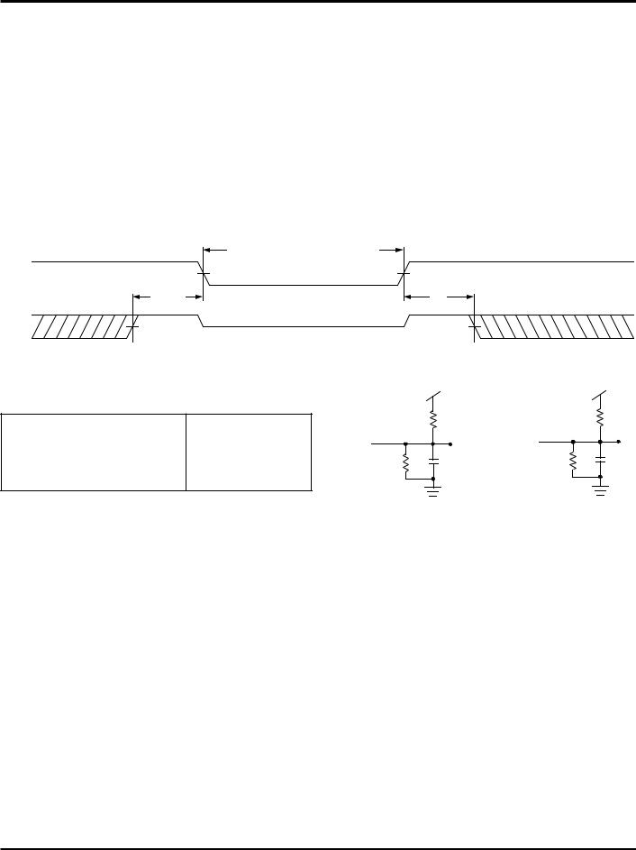
DATA RETENTION WAVEFORM
Vcc
4.5V
|
tCDR |
CE |
VIH |
|
DATA RETENTION MODE |
|
VDR ³ 2V |
4.5V |
|
tR |
VDR |
VIH |
|
|
|
|
|
|
2654 drw 03 |
AC TEST CONDITIONS |
|
5V |
|
|
5V |
|
|
|
|
|
|
Input Pulse Levels |
GND to 3.0V |
|
1250Ω |
|
1250Ω |
|
|
|
|||
Input Rise/Fall Times |
5ns |
DATAOUT |
|
DATAOUT |
|
Input Timing Reference Levels |
1.5V |
BUSY |
|
|
|
INT |
|
775Ω |
5pF |
||
Output Reference Levels |
1.5V |
775Ω |
30pF |
||
|
|
|
|
||
Output Load |
Figures 1 and 2 |
|
|
|
|
2654 drw 04
2654 tbl 07
Figure 1. AC Output Test Load Figure 2. Output Test Load
(For tLZ, tHZ, tWZ, tOW) Including scope and jig.
AC ELECTRICAL CHARACTERISTICS OVER THE
OPERATING TEMPERATURE AND SUPPLY VOLTAGE RANGE(3)
|
|
70121X25 |
70121X35 |
70121X45 |
70121X55 |
|
||||
|
|
70125X25 |
70125X35 |
70125X45 |
70125X55 |
|
||||
Symbol |
Parameter |
|
|
|
|
|
|
|
|
Unit |
Min. |
Max. |
Min. |
Max. |
Min. |
Max. |
Min. |
Max. |
|||
|
|
|
|
|
|
|
|
|
|
|
Read Cycle |
|
|
|
|
|
|
|
|
|
|
|
|
|
|
|
|
|
|
|
|
|
tRC |
Read Cycle Time |
25 |
— |
35 |
— |
45 |
— |
55 |
— |
ns |
|
|
|
|
|
|
|
|
|
|
|
tAA |
Address Access Time |
— |
25 |
— |
35 |
— |
45 |
— |
55 |
ns |
|
|
|
|
|
|
|
|
|
|
|
tACE |
Chip Enable Access Time |
— |
25 |
— |
35 |
— |
45 |
— |
55 |
ns |
|
|
|
|
|
|
|
|
|
|
|
tAOE |
Output Enable Access Time |
— |
12 |
— |
25 |
— |
30 |
— |
35 |
ns |
|
|
|
|
|
|
|
|
|
|
|
tOH |
Output Hold from Address Change |
0 |
— |
0 |
— |
0 |
— |
0 |
— |
ns |
tLZ |
Output Low-Z Time(1,2) |
0 |
— |
0 |
— |
0 |
— |
0 |
— |
ns |
tHZ |
Output High-Z Time(1,2) |
— |
10 |
— |
15 |
— |
20 |
— |
30 |
ns |
tPU |
Chip Enable to Power-Up Time(2) |
0 |
— |
0 |
— |
0 |
— |
0 |
— |
ns |
tPD |
Chip Disable to Power-Down Time(2) |
— |
50 |
— |
50 |
— |
50 |
— |
50 |
ns |
NOTES: |
|
|
|
|
|
|
|
|
2654 tbl 08 |
|
1.Transition is measured ±500mV from Low or High-impedance voltage with the Output Test Load (Figure 2).
2.This parameter guaranteed by device characterization, but is not production tested.
3.“X” in part numbers indicates power rating (S or L).
6.10 |
4 |
 Loading...