


Integrated Device Technology Inc. IDT54FCT16501AT, IDT54FCT16501CT, IDT54FCT16501ET, IDT54FCT162501AT, IDT54FCT162501CT User Manual
...IDT54FCT240ADB
®
Integrated Device Technology, Inc.
FAST CMOS OCTAL |
IDT54/74FCT240/A/C |
|
IDT54/74FCT241/A/C |
||
BUFFER/LINE DRIVER |
||
IDT54/74FCT244/A/C |
||
|
IDT54/74FCT540/A/C |
|
|
IDT54/74FCT541/A/C |
|
|
|
FEATURES:
•IDT54/74FCT240/241/244/540/541 equivalent to FASTTM speed and drive
•IDT54/74FCT240A/241A/244A/540A/541A 25% faster than FAST
•IDT54/74FCT240C/241C/244C/540C/541C up to 55% faster than FAST
•IOL = 64mA (commercial) and 48mA (military)
•CMOS power levels (1mW typ. static)
•Product available in Radiation Tolerant and Radiation Enhanced versions
•Military product compliant to MIL-STD-883, Class B
•Meets or exceeds JEDEC Standard 18 specifications
DESCRIPTION:
The IDT octal buffer/line drivers are built using an advanced dual metal CMOS technology. The IDT54/74FCT240/A/C, IDT54/74FCT241/A/C and IDT54/74FCT244/A/C are designed to be employed as memory and address drivers, clock drivers and bus-oriented transmitter/receivers which provide improved board density.
The IDT54/74FCT540/A/C and IDT54/74FCT541/A/C are similar in function to the IDT54/74FCT240/A/C and IDT54/ 74FCT244/A/C, respectively, except that the inputs and outputs are on opposite sides of the package. This pinout arrangement makes these devices especially useful as output ports for microprocessors and as backplane drivers, allowing ease of layout and greater board density.
FUNCTIONAL BLOCK DIAGRAMS 2529 cnv* 01–03
OEA |
|
OEA |
241 Only |
|
OEB |
|
OEB* |
DA0 |
OA0 |
DA0 |
OA0 |
OB0 |
DB0 |
OB0 |
DB0 |
DA1 |
OA1 |
DA1 |
OA1 |
OB1 |
DB1 |
OB1 |
DB1 |
DA2 |
OA2 |
DA2 |
OA2 |
OB2 |
DB2 |
OB2 |
DB2 |
DA3 |
OA3 |
DA3 |
OA3 |
OB3 |
DB3 |
OB3 |
DB3 |
|
IDT54/74FCT240 |
|
IDT54/74FCT241/244 |
|
|
|
*OEB for 241, OEB for 244 |
OEA 
 OEB
OEB
D0  O0* D1
  O1* D2
  O2* D3
  O3* D4
  O4* D5
  O5* D6
  O6* D7
  O7*
O7*
IDT54/74FCT540/541
*Logic diagram shown for 'FCT540. 'FCT541 is the non-inverting option.
2606 dwg 01–03
The IDT logo is a registered trademark of Integrated Device Technology, Inc.
FAST is a trademark of National Semiconductor Co.
MILITARY AND COMMERCIAL TEMPERATURE RANGES |
MAY 1992 |
|
©1992 Integrated Device Technology, Inc. |
7.8 |
DSC-4610/3 |
1

IDT54/74FCT240/241/244/540/541/A/C
FAST CMOS OCTAL BUFFER/LINE DRIVER
PIN CONFIGURATIONS
IDT54/74FCT240
2529 cnv* 04–09
OEA |
|
1 |
|
20 |
|
VCC |
DA0 |
|
2 |
|
19 |
|
OEB |
|
|
|
||||
OB0 |
|
3 |
|
18 |
|
OA0 |
|
|
|
||||
DA1 |
|
4 |
P20-1 |
17 |
|
DB0 |
|
|
|||||
|
|
|
|
|
||
OB1 |
|
5 |
D20-1 |
16 |
|
OA1 |
|
|
|||||
DA2 |
|
6 |
SO20-2 |
15 |
|
DB1 |
|
|
|||||
OB2 |
|
7 |
& |
14 |
|
OA2 |
|
|
|||||
|
|
|||||
|
E20-1 |
|
||||
DA3 |
|
8 |
13 |
|
DB2 |
|
|
|
|
||||
OB3 |
|
9 |
|
12 |
|
OA3 |
|
|
|
||||
GND |
|
10 |
|
11 |
|
DB3 |
|
|
|
||||
|
DIP/SOIC/CERPACK |
|
||||
|
|
|
TOP VIEW |
|
||
IDT54/74FCT241/244
OEA |
1 |
|
20 |
VCC |
|
DA0 |
2 |
|
19 |
OEB* |
|
OB0 |
3 |
|
18 |
OA0 |
|
DA1 |
4 |
P20-1 |
17 |
DB0 |
|
|
|
|
|
||
OB1 |
5 |
D20-1 |
16 |
OA1 |
|
DA2 |
6 |
SO20-2 |
15 |
DB1 |
|
OB2 |
7 |
& |
14 |
OA2 |
|
E20-1 |
|||||
DA3 |
8 |
13 |
DB2 |
||
|
|||||
OB3 |
9 |
|
12 |
OA3 |
|
GND |
10 |
|
11 |
DB3 |
|
|
DIP/SOIC/CERPACK |
|
|||
|
|
TOP VIEW |
|
||
*OEB for 241, OEB for 244 |
|
|
|
||
IDT54/74FCT540/541
OEA |
1 |
|
20 |
VCC |
|
D0 |
2 |
|
19 |
OEB |
|
D1 |
3 |
|
18 |
O0* |
|
D2 |
4 |
P20-1 |
17 |
O1* |
|
|
|
|
|
||
D3 |
5 |
D20-1 |
16 |
O2* |
|
D4 |
6 |
SO20-2 |
15 |
O3* |
|
D5 |
7 |
& |
14 |
O4* |
|
E20-1 |
|||||
D6 |
8 |
13 |
O5* |
||
|
|||||
D7 |
9 |
|
12 |
O6* |
|
GND |
10 |
|
11 |
O7* |
DIP/SOIC/CERPACK
TOP VIEW
*OX for 540, OX for 541
MILITARY AND COMMERCIAL TEMPERATURE RANGES
INDEX |
OB0 |
DA0 |
OEA |
VCC |
OEB |
|
|
|
|||||
|
3 |
2 |
1 |
20 19 |
|
|
DA1 |
4 |
|
|
18 |
OA0 |
|
|
|
|
||||
OB1 |
5 |
|
|
|
17 |
DB0 |
DA2 |
6 |
L20-2 |
16 |
OA1 |
||
OB2 |
7 |
|
|
|
15 |
DB1 |
DA3 |
8 |
|
|
|
14 |
OA2 |
|
9 |
10 11 12 13 |
|
|||
|
OB3 |
GND |
DB3 |
OA3 |
DB2 |
|
|
|
|
LCC |
|
|
|
|
|
TOP VIEW |
|
|
||
INDEX |
|
|
|
|
* |
|
OB0 |
DA0 |
OEA |
VCC |
OEB |
|
|
|
|
|||||
|
3 |
2 |
1 |
20 19 |
|
|
DA1 |
4 |
|
|
18 |
OA0 |
|
|
|
|
||||
OB1 |
5 |
|
|
|
17 |
DB0 |
DA2 |
6 |
L20-2 |
16 |
OA1 |
||
OB2 |
7 |
|
|
|
15 |
DB1 |
DA3 |
8 |
|
|
|
14 |
OA2 |
|
9 |
10 11 12 13 |
|
|||
|
OB3 |
GND |
DB3 |
OA3 |
DB2 |
|
|
|
|
LCC |
|
|
|
|
|
TOP VIEW |
|
|
||
INDEX |
D1 |
D0 |
OEA |
VCC |
OEB |
|
|
|
|||||
|
3 |
2 |
1 |
20 19 |
|
|
D2 |
4 |
|
|
18 |
O0* |
|
|
|
|
||||
D3 |
5 |
|
|
|
17 |
O1* |
D4 |
6 |
L20-2 |
16 |
O2* |
||
D5 |
7 |
|
|
|
15 |
O3* |
D6 |
8 |
|
|
|
14 |
O4* |
|
9 |
10 11 12 13 |
|
|||
|
D7 |
GND |
O7* |
O6* |
O5* |
|
|
|
|
LCC |
|
|
|
|
|
TOP VIEW |
|
2606 cnv* 04–09 |
||
7.8 |
2 |
IDT54/74FCT240/241/244/540/541/A/C |
|
FAST CMOS OCTAL BUFFER/LINE DRIVER |
MILITARY AND COMMERCIAL TEMPERATURE RANGES |
|
|
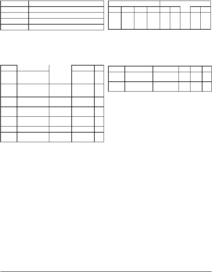
PIN DESCRIPTION |
FUNCTION TABLE |
Pin Names |
Description |
OEA, OEB |
3–State Output Enable Inputs (Active LOW) |
OEB(1) |
3–State Output Enable Input (Active HIGH) |
Dxx |
Inputs |
Oxx |
Outputs |
NOTE: |
2606 tbl 04 |
1. OEB for 241 only.
|
Inputs(1) |
|
|
Outputs(1) |
|
|||
OEA |
OEB |
OEB(2) |
D |
240 |
241 |
244 |
540 |
541 |
L |
L |
H |
L |
H |
L |
L |
H |
L |
L |
L |
H |
H |
L |
H |
H |
L |
H |
H |
H |
L |
X |
Z |
Z |
Z |
Z |
Z |
NOTES: |
|
|
|
|
|
|
|
2606 tbl 05 |
1.H = High Voltage Level X = Don’t Care
L = Low Voltage Level Z = High Impedance
2.OEB for 241 only.
ABSOLUTE MAXIMUM RATINGS(1)
Symbol |
Rating |
Commercial |
Military |
Unit |
VTERM(2) |
Terminal Voltage |
–0.5 to +7.0 |
–0.5 to +7.0 |
V |
|
with Respect to |
|
|
|
|
GND |
|
|
|
VTERM(3) |
Terminal Voltage |
–0.5 to VCC |
–0.5 to VCC |
V |
|
with Respect to |
|
|
|
|
GND |
|
|
|
TA |
Operating |
0 to +70 |
–55 to +125 |
°C |
|
Temperature |
|
|
|
TBIAS |
Temperature |
–55 to +125 |
–65 to +135 |
°C |
|
Under Bias |
|
|
|
TSTG |
Storage |
–55 to +125 |
–65 to +150 |
°C |
|
Temperature |
|
|
|
PT |
Power Dissipation |
0.5 |
0.5 |
W |
IOUT |
DC Output |
120 |
120 |
mA |
|
Current |
|
|
|
NOTES: |
|
|
2606 tbl 01 |
|
1.Stresses greater than those listed under ABSOLUTE MAXIMUM RATINGS may cause permanent damage to the device. This is a stress rating only and functional operation of the device at these or any other conditions above those indicated in the operational sections of this specification is not implied. Exposure to absolute maximum rating conditions for extended periods may affect reliability. No terminal voltage may exceed VCC by +0.5V unless otherwise noted.
2.Input and VCC terminals only.
3.Outputs and I/O terminals only.
CAPACITANCE (TA = +25°C, f = 1.0MHz)
Symbol |
Parameter (1) |
Conditions |
Typ. |
Max. |
Unit |
CIN |
Input |
VIN = 0V |
6 |
10 |
pF |
|
Capacitance |
|
|
|
|
COUT |
Output |
VOUT = 0V |
8 |
12 |
pF |
|
Capacitance |
|
|
|
|
NOTE: |
|
|
|
|
2606 tbl 02 |
1. This parameter is measured at characterization but not tested.
7.8 |
3 |
 Loading...