


Integrated Device Technology Inc IDT79RV464080MUI, IDT79RV464080MU, IDT79RV4640133DU, IDT79RV4640100MUI, IDT79RV4640100MU Datasheet
...
LOW-COST EMBEDDED |
|
ORION™ RISC |
IDT79R4640™ |
MICROPROCESSOR |
IDT79RV4640™ |
Integrated Device Technology, Inc.
FEATURES
•High-performance embedded 64-bit microprocessor
-64-bit integer operations
-64-bit registers
-Based on the MIPS RISC Architecture
-80MHz, 100MHz, 133 MHz and 150MHz operation frequency
-32-bit bus interface brings 64-bit power to 32-bit system cost
•High-performance DSP capability
-75 Million Integer Mul-Accumulate operations/sec @150MHz
-50 MFlops floating-point operations @150MHz
•High-performance microprocessor
-75 M Mul-Add/second @150MHz
-50 MFlops @150MHz
->340,000 dhrystone (2.1)/sec capability @133MHz (197 dhrystone MIPS)
•High level of integration
-64-bit, 150 MHz integer CPU
-50MFlops single-precision floating-point unit
-8KB instruction cache; 8KB data cache
-Integer multiply unit with 75M Mul-Add/sec
•Upwardly software compatible with IDT RISController Family
•Easily upgradable to 64-bit system
•Low-power operation
-Active power management powers-down inactive units
-Standby mode
•Large, efficient on-chip caches
-Separate 8KB Instruction and 8KB Data caches
-Over 1800MB/sec bandwidth from internal caches
-2-set associative
-Write-back and write-through support
-Cache locking to facilitate deterministic response
-High performance write protocols for graphics and data communications
•Bus compatible with ORION family
-System interfaces to 67 MHz, provides bandwidth up to 266 MB/sec
-Direct interface to 32-bit wide systems
-Synchronized to external reference clock for multimaster operation
•Improved real-time support
-Fast interrupt decode
-Optional cache locking
BLOCK DIAGRAM
150 MHz 64-bit ORION CPU |
System Control Coprocessor |
50MFlops Single-Precision FPA |
|||||||
|
|
|
|
|
|
|
|
|
|
|
64-bit Register File |
|
|
Address Translation/ |
|
|
|
FP Register File |
|
|
|
|
|
Cache Attribute Control |
|
|
|
|
|
|
64-bit Adder |
ControlPipeline |
|
|
|
|
ControlPipeline |
Pack/Unpack |
|
|
|
|
|
|
|
||||
|
|
|
|
|
|
|
|||
|
|
|
|
|
|
|
|
|
|
|
Load Aligner |
|
|
Exception Management |
|
|
|
|
|
|
|
|
|
|
|
||||
|
|
|
|
Functions |
|
|
|
FP Add/Sub/Cvt/ |
|
|
Store Aligner |
|
|
|
|
||||
|
|
|
|
|
|
|
|
||
|
|
|
|
|
|
|
|
Div/Sqrt |
|
|
Logic Unit |
|
|
|
|
|
|
|
|
|
|
|
|
|
|
|
|
|
|
|
|
|
|
|
|
|
|
|
|
|
High-Performance |
|
|
|
|
|
|
FP Multiply |
|
|
Integer Multiply |
|
|
|
|
|
|
|
|
|
|
|
|
|
|
|
|
|
|
|
|
|
|
|
|
|
|
|
|
Control Bus |
Data Bus |
Instruction Bus |
|
|
|
|
|
|
|
|
|
|
|
|
|
Instruction Cache |
|
|
|
|
|
|
|
|
|
|
|
|
|
|
|
|
|
|
|
|
||
|
Set A |
|
|
|
|
|
|
Data Cache |
|
||
|
(Lockable) |
|
|
|
|
|
|
Set A |
|
||
|
|
|
|
|
|
|
|
|
(Lockable) |
|
|
|
Instruction Cache |
|
|
|
|
32-bit |
|
|
|
|
|
|
|
|
|
|
|
Data Cache |
|
|
|||
|
|
|
|
|
Synchronized |
|
|
|
|||
|
Set B |
|
|
|
|
|
|
||||
|
|
|
|
|
|
Set B |
|
|
|||
|
|
|
|
|
|
System Interface |
|
|
|||
|
|
|
|
|
|
|
|
|
|
||
|
|
|
|
|
|
|
|
|
|
|
|
The IDT logo is a registered trademark and ORION, R4650, R4640, RV4640, R4600, R3081, R3052, R3051, R3041, R5000, R36100 , RISController, and RISCore |
|||||||||||
are trademarks of Integrated Device Technology, Inc. |
|
|
|
|
|
|
|||||
|
|
|
|
|
|
|
|
|
|
|
|
COMMERCIAL/INDUSTRIAL TEMPERATURE RANGE |
|
MAY 1997 |
|
||||||||
1997 Integrated Device Technology, Inc. |
|
|
|
3486/1 |
|||||||
|
|
|
1 |
|
|||||||

R4640/RV4640 |
|
|
|
|
|
|
|
COMMERCIAL/INDUSTRIAL TEMPERATURE RANGE |
|
|
DESCRIPTION |
|
|
|
|
|
|
R4640 is software-compatible with the R4650, and |
|||
The IDT79R4640 |
is a |
low-cost |
member of |
the |
includes the instruction set found in the R4700 micropro- |
|||||
cessor, targeted at higher performance while maintaining |
||||||||||
Integrated Device Technology, Inc. ORION family, targeted |
||||||||||
binary compatibility with earlier R30xx processors. The |
||||||||||
to a variety of performance-hungry embedded applica- |
||||||||||
extensions result in better code density, greater multi- |
||||||||||
tions. The R4640 continues the ORION tradition of high- |
||||||||||
processing support, improved performance for commonly |
||||||||||
performance through |
high-speed pipelines, high-band- |
|||||||||
used code sequences in operating system kernels, and |
||||||||||
width caches and bus interface, 64-bit architecture, and |
||||||||||
faster execution of floating-point intensive applications. All |
||||||||||
careful attention |
to efficient |
control. The cost |
of |
this |
||||||
performance is |
reduced by |
removing |
functional |
units |
resource dependencies are made transparent to the |
|||||
programmer, insuring transportability among implementa- |
||||||||||
frequently not required for many embedded applications. |
||||||||||
tions of the MIPS instruction set architecture. In addition, |
||||||||||
The R4640 |
supports a wide variety of embedded |
|||||||||
MIPS-III specifies new instructions defined to take |
||||||||||
processor-based applications, such as internetworking |
||||||||||
advantage of the 64-bit architecture of the processor. |
||||||||||
equipment (routers, switches), office automation equip- |
||||||||||
ment (printers, |
scanners), and consumer multimedia |
Finally, the R4640 also implements additional instruc- |
||||||||
tions, which are considered extensions to the MIPS-III |
||||||||||
game systems. Also, being upwardly software-compatible |
||||||||||
architecture. These instructions improve the multiply and |
||||||||||
with the RISController family as well as busand upwardly |
||||||||||
multiply-add throughput of the CPU, making it well suited |
||||||||||
software-compatible with the IDT ORION family, the R4640 |
||||||||||
to a wide variety of imaging and DSP applications. These |
||||||||||
will serve in many of |
the same applications. And, |
the |
||||||||
extensions, which use opcodes allocated by MIPS |
||||||||||
R4640 supports applications that require integer digital |
||||||||||
Technologies for this purpose, are supported by a wide |
||||||||||
signal processing (DSP) functions. |
|
|
|
|
||||||
|
|
|
|
variety of development tools. |
||||||
The R4640 brings ORION performance levels to lower |
||||||||||
The MIPS integer unit implements a load/store archi- |
||||||||||
cost systems. ORION |
performance |
is |
preserved |
by |
||||||
tecture with single cycle ALU operations (logical, shift, |
||||||||||
retaining large on-chip two-way set-associative caches, a |
||||||||||
add, sub) and autonomous multiply/divide unit. The 64-bit |
||||||||||
streamlined high-speed pipeline, high bandwidth, 64-bit |
||||||||||
register resources include: 32 general-purpose |
||||||||||
execution, and facilities such |
as early |
restart for data |
||||||||
orthogonal integer registers, the HI/LO result registers for |
||||||||||
cache misses. |
|
|
|
|
|
|
|
|||
|
|
|
|
|
|
|
the integer multiply/divide unit, and the program counter. |
|||
These techniques allow the system designer over 1.8 |
||||||||||
In addition, the on-chip floating-point co-processor adds |
||||||||||
GB/sec aggregate internal bandwidth, 266 MB/sec bus |
||||||||||
32 floating-point registers, and a floating-point |
||||||||||
bandwidth, almost 200 Dhrystone MIPS, 50MFlops, and |
||||||||||
control/status register. |
||||||||||
75 M Mul-Add/sec. An array of tools facilitates rapid |
||||||||||
|
|
|||||||||
development of R4640-based systems, allowing a wide |
Register File |
|||||||||
variety of customers access to the processor’s high- |
The R4640 has 32 general-purpose 64-bit registers. |
|||||||||
performance capabilities while maintaining short time-to- |
These registers are used for scalar integer operations and |
|||||||||
market goals. |
|
|
|
|
|
|
|
address calculation. The register file consists of two read |
||
HARDWARE OVERVIEW |
|
|
|
|
ports and one write port and is fully bypassed to minimize |
|||||
|
|
|
|
operation latency in the pipeline. |
||||||
Some key elements of the R4640 are briefly described below. More detailed information is available in the IDT79R4640/IDT79R4650 RISC Processor Hardware User’s Manual.
Pipeline
The R4640 uses a 5-stage pipeline that is similar to the IDT79R3000 and the IDT79R4700 processors. The simplicity of this pipeline allows the R4640 to cost less than super-scalar processors and require less power than super-pipelined processors. So, unlike superscalar processors, applications that have large data dependencies or require a great deal of load/stores can still achieve peak performance.
Integer Execution Engine
The R4640 implements the MIPS-III Instruction Set Architecture, and thus is fully upward compatible with applications running on the earlier generation parts. The
R4640/RV4640 |
COMMERCIAL/INDUSTRIAL TEMPERATURE RANGE |
Opcode |
Operand |
Latency |
Repeat |
Stall |
|
|
Size |
|
|
|
|
|
|
|
|
|
|
|
|
|
|
|
|
M U L T / U , |
16 bit |
3 |
2 |
0 |
|
MAD/U |
|
|
|
|
|
32 bit |
4 |
3 |
0 |
||
|
|||||
|
|
|
|
|
|
MUL |
16 bit |
3 |
2 |
1 |
|
|
|
|
|
|
|
|
32 bit |
4 |
3 |
2 |
|
|
|
|
|
|
|
D M U L T, |
any |
6 |
5 |
0 |
|
DMULTU |
|
|
|
|
|
|
|
|
|
|
|
DIV, DIVU |
any |
36 |
36 |
0 |
|
|
|
|
|
|
|
D D I V, |
any |
68 |
68 |
0 |
|
DDIVU |
|
|
|
|
|
|
|
|
|
|
|
Table 1: R4640 Integer Multiply Operation |
|
||||
The floating-point unit of the R4640 directly implements single-precision floating-point operations, which enables the R4640 to perform functions such as graphics rendering without requiring extensive die area or power consumption. The single-precision unit of the R4640 is directly compatible with the single-precision operation of the R4700, and features the same latencies and repeat rates.
The R4640 does not directly implement the doubleprecision operations found in the R4700. However, to maintain software compatibility, the R4640 will signal a trap when a double-precision operation is initiated, allowing the requested function to be emulated in software. Alternatively, the system architect could use a software library emulation of double-precision functions, selected at compile time, to eliminate the overhead associated with trap and emulation.
Floating-Point Units
The MIPS-III architecture defines that the results of a |
The R4640’s floating-point execution units perform |
|
multiply or divide operation are placed in the HI and LO |
||
single precision arithmetic, as specified in IEEE Standard |
||
registers. The values can then be transferred to the |
||
754. The execution unit is broken into a separate multiply |
||
general purpose register file using the MFHI/MFLO |
||
unit and a combined add/convert/divide/square root unit. |
||
instructions. |
||
Overlap of multiply and add/subtract is supported. The |
||
|
The R4640 adds a new multiply instruction, “MUL”, multiplier is partially pipelined, allowing a new multiplica-
which can specify that the multiply results bypass the “Lo” tion instruction to begin every 6 cycles. |
|
register and are placed immediately in the primary |
As in the IDT79R4700, the R4640 maintains fully |
register file. By avoiding the explicit “Move-from-Lo” precise floating-point exceptions while allowing both
instruction required when using “Lo”, throughput of overlapped and pipelined operations. Precise exceptions |
|||
multiply-intensive operations is increased. |
are extremely important in mission-critical environments, |
||
An additional enhancement offered by the R4640 is an |
|||
such as ADA, and highly desirable for debugging in any |
|||
|
|||
atomic “multiply-add” operation, MAD, used to perform environment. |
|||
multiply-accumulate operations. This instruction multiplies |
The floating-point unit’s operation set includes floating- |
||
two numbers and adds the product to the current contents |
|||
point add, subtract, multiply, divide, square root, |
|||
of the HI and LO registers. This operation is used in |
|||
conversion between fixed-point and floating-point format, |
|||
numerous DSP algorithms, and allows the R4640 to cost |
|||
conversion among floating-point formats, and floating- |
|||
reduce systems requiring a mix of DSP and control |
|||
point compare. These operations comply with IEEE |
|||
functions. |
|||
Standard 754. Double precision operations are not |
|||
Finally, aggressive implementation techniques feature |
|||
directly supported; attempts to execute double-precision |
|||
low latency for these operations along with pipelining to |
|||
floating point operations, or refer directly to double- |
|||
allow new operations to be issued before a previous one |
|||
precision registers, result in the R4640 signalling a “trap” |
|||
has fully completed. Table 1 also shows the repeat rate |
|||
to the CPU, enabling emulation of the requested function. |
|||
(peak issue rate), latency, and number of processor stalls |
|||
|
|
||
required for the various operations. The R4640 performs |
|
|
|
automatic operand size detection to determine the size of |
|
|
|
the operand, and implements hardware interlocks to |
|
|
|
prevent overrun, allowing this high-performance to be |
|
|
|
achieved with simple programming. |
|
|
|
Floating-Point Coprocessor |
|
|
|
The R4640 incorporates an entire single-precision |
|
|
|
floating-point coprocessor on chip, including a floating- |
|
|
|
point register file and execution units. The floating-point |
|
|
|
coprocessor forms a “seamless” interface with the integer |
|
|
|
unit, decoding and executing instructions in parallel with |
|
|
|
the integer unit. |
|
|
|
|
|
|
|
|
3 |
|
|

R4640/RV4640 COMMERCIAL/INDUSTRIAL TEMPERATURE RANGE
Table 2 gives the latencies of some of the floating-point |
System Control Coprocessor Registers |
||||||
instructions in internal processor cycles. |
The R4640 incorporates all system control co- |
||||||
|
|
|
|
processor (CP0) registers on-chip. These registers |
|||
|
Operation |
Instruction |
|
provide the path through which the virtual memory |
|||
|
|
system’s address translation is controlled, exceptions are |
|||||
|
Latency |
|
|||||
|
|
|
handled, and operating modes are controlled (kernel vs. |
||||
|
|
|
|
||||
|
|
|
|
user mode, interrupts enabled or disabled, cache |
|||
|
ADD |
4 |
|
||||
|
|
|
|
features). In addition, the R4640 includes registers to |
|||
|
SUB |
4 |
|
||||
|
|
implement a real-time cycle counting facility, which aids in |
|||||
|
|
|
|
||||
|
MUL |
8 |
|
cache diagnostic testing, assists in data error detection, |
|||
|
|
and facilitates software debug. Alternatively, this timer |
|||||
|
|
|
|
||||
|
DIV |
32 |
|
||||
|
|
can be used as the operating system reference timer, and |
|||||
|
|
|
|
can signal a periodic interrupt. |
|||
|
SQRT |
31 |
|
||||
|
|
Table 3 shows the CP0 registers of the R4640. |
|||||
|
|
|
|
||||
|
CMP |
3 |
|
|
|
|
|
|
|
|
|
Number |
Name |
Function |
|
|
FIX |
4 |
|
||||
|
|
|
|
|
|||
|
|
|
|
|
|
|
|
|
|
|
|
0 |
IBase |
Instruction address space base (new in |
|
|
FLOAT |
6 |
|
||||
|
|
|
|
R4640) |
|||
|
|
|
|
|
|
|
|
|
|
|
|
|
|
|
|
|
ABS |
1 |
|
1 |
IBound |
Instruction address space bound (new |
|
|
|
|
|
|
|
in R4640) |
|
|
MOV |
1 |
|
|
|
||
|
|
|
|
|
|||
|
|
2 |
DBase |
Data address space base (new in |
|||
|
|
|
|
||||
|
NEG |
1 |
|
|
|
R4640) |
|
|
|
|
|
|
|||
|
|
|
|
|
|
|
|
|
|
|
|
3 |
DBound |
Data address space bound (new in |
|
|
LWC1 |
2 |
|
||||
|
|
|
|
R4640) |
|||
|
|
|
|
|
|
||
|
SWC1 |
1 |
|
|
|
|
|
|
|
4-7, 10, |
- |
Not used |
|||
|
|
|
|
20-25, |
|
|
|
|
Table 2: Floating-Point Operation |
|
|
||||
|
29, 31 |
|
|
||||
|
|
|
|
|
|
||
Floating-Point General Register File |
|
|
|
||||
8 |
BadVAddr |
Virtual address on address exceptions |
|||||
The floating-point register file is made up of thirty-two |
|
|
|
||||
9 |
Count |
Counts every other cycle |
|||||
32-bit registers. These registers are used as source or |
|||||||
|
|
|
|||||
11 |
Compare |
Generate interrupt when Count = |
|||||
target registers for the single-precision operations. |
|||||||
|
|
Compare |
|||||
References to these registers as 64-bit registers (as |
|
|
|||||
|
|
|
|||||
supported in the R4700) will cause a trap to be signalled |
12 |
Status |
Miscellaneous control/status |
||||
|
|
|
|||||
to the integer unit. |
|
|
13 |
Cause |
Exception/Interrupt information |
||
The floating-point control register space contains two |
|
|
|
||||
14 |
EPC |
Exception PC |
|||||
registers; one for determining configuration and revision |
|
|
|
||||
15 |
PRId |
Processor ID |
|||||
information for the coprocessor and one for control and |
|||||||
|
|
|
|||||
status information. These are primarily involved with |
16 |
Config |
Cache and system attributes |
||||
|
|
|
|||||
diagnostic software, exception handling, state saving and |
17 |
CAlg |
Cache attributes for the 8 512MB |
||||
restoring, and control of rounding modes. |
|
|
regions of the virtual address space |
||||
|
|
|
|
|
|
|
|
System Control Coprocessor (CP0) |
18 |
IWatch |
Instruction breakpoint virtual address |
||||
|
|
|
|||||
The system control coprocessor in the MIPS archi- |
19 |
DWatch |
Data breakpoint virtual address |
||||
tecture is responsible for the virtual to physical address |
|
|
|
||||
26 |
ECC |
Used in cache diagnostics |
|||||
translation and cache protocols, the exception control |
|
|
|
||||
27 |
CacheErr |
Cache diagnostic information |
|||||
system, and the diagnostics capability of the processor. In |
|||||||
|
|
|
|||||
28 |
TagLo |
Cache index information |
|||||
the MIPS architecture, the system control coprocessor |
|||||||
|
|
|
|||||
(and thus the kernel software) is implementation |
30 |
ErrorEPC |
CacheError exception PC |
||||
dependent. |
|
|
|
|
|
||
|
|
|
Table 3: R4640 CPO Registers |
||||
In the R4640, significant changes in CP0 relative to the |
|
||||||
Operation modes |
|
||||||
R4600 have been implemented. These changes are |
|
||||||
designed to simplify memory management, facilitate |
The R4640 supports two modes of operation: user |
||||||
debug, and speed real-time processing. |
mode and kernel mode. |
||||||
|
|
|
|
Kernel mode operation is typically used for exception |
|||
|
|
|
|
handling and operating system kernel functions, including |
|||
|
|
|
|
|
|
|
|
|
|
|
|
|
|
4 |
|

R4640/RV4640 |
COMMERCIAL/INDUSTRIAL TEMPERATURE RANGE |
CP0 management and access to IO devices. In kernel mode, software has access to the entire address space and all of the co-processor 0 registers, and can select whether to enable co-processor 1 accesses. The processor enters kernel mode at reset, and whenever an exception is recognized.
User mode is typically used for applications programs. User mode accesses are limited to a subset of the virtual address space, and can be inhibited from accessing CP0 functions.
0xFFFFFFFF
Kernel virtual address space (kseg2)
Unmapped, 1.0 GB
0xC0000000
0xBFFFFFFF
Uncached kernel physical address space (kseg1)
Unmapped, 0.5GB
0xA0000000
0x9FFFFFFF
Cached kernel physical address space (kseg0)
Unmapped, 0.5GB
0x80000000
0x7FFFFFF
User virtual address space (useg)
Mapped, 2.0GB
0x00000000
Figure 3: Mode Virtual Addressing (32-bit mode)
the virtual address to form the physical address for that reference. If the address is not within bounds, an exception is signalled.
This facility enables multiple user processes in a single physical memory without the use of a TLB. This type of operation is further supported by a number of development tools for the R4640, including real-time operating systems and “position independent code”.
Kernel mode addresses do not use the base-bounds registers, but rather undergo a fixed virtual to physical address translation.
Debug Support
To facilitate software debug, the R4640 adds a pair of “watch” registers to CP0. When enabled, these registers will cause the CPU to take an exception when a “watched” address is appropriately accessed.
Interrupt Vector
The R4640 also adds the capability to speed interrupt exception decoding. Unlike the R4700, which utilizes a single common exception vector for all exception types (including interrupts), the R4640 allows kernel software to enable a separate interrupt exception vector. When enabled, this vector location speeds interrupt processing by allowing software to avoid decoding interrupts from general purpose exceptions.
Cache Memory
To keep the R4640’s high-performance pipeline full and operating efficiently, the R4640 incorporates on-chip instruction and data caches that can each be accessed in a single processor cycle. Each cache has its own 64-bit data path and can be accessed in parallel. The cache subsystem provides the integer and floating-point units with an aggregate bandwidth of over 1800 MB per second at a pipeline clock frequency of 150MHz. The cache subsystem is similar in construction to that found in the R4600, although some changes have been implemented. Table 6 is an overview of the caches found on the R4640.
Virtual-to-Physical Address Mapping |
Instruction Cache |
|
The R4640 incorporates a two-way set associative on- |
||
The 4GB virtual address space of the R4640 is shown |
||
chip instruction cache. This virtually indexed, physically |
||
in figure 3. The 4 GB address space is divided into |
||
tagged cache is 8KB in size and is parity protected. |
||
addresses accessible in either kernel or user mode |
||
Because the cache is virtually indexed, the virtual-to- |
||
(kuseg), and addresses only accessible in kernel mode |
||
physical address translation occurs in parallel with the |
||
(kseg2:0). |
||
cache access, thus further increasing performance by |
||
The R4640 supports the use of multiple user tasks |
||
allowing these two operations to occur simultaneously. |
||
sharing common virtual addresses, but mapped to |
||
The tag holds a 20-bit physical address and valid bit, and |
||
separate physical addresses. This facility is implemented |
||
is parity protected. |
||
via the “base-bounds” registers contained in CP0. |
||
The instruction cache is 64-bits wide, and can be |
||
When a user virtual address is asserted (load, store, or |
||
refilled or accessed in a single processor cycle. |
||
instruction fetch), the R4640 compares the virtual address |
||
|
with the contents of the appropriate “bounds” register Instruction fetches require only 32 bits per cycle, for a (instruction or data). If the virtual address is “in bounds”, peak instruction bandwidth of 600MB/sec at 150MHz. the value of the corresponding “base” register is added to Sequential accesses take advantage of the 64-bit fetch to reduce power dissipation, and cache miss refill, can write
5
R4640/RV4640 |
|
|
|
|
COMMERCIAL/INDUSTRIAL TEMPERATURE RANGE |
64 bits-per-cycle to minimize the cache miss penalty. The |
|
without changing cache contents. |
|||
line size is eight instructions (32 bytes) to maximize |
• |
Writeback. Loads and instruction fetches will first |
|||
performance. |
|
|
|
|
search the cache, reading main memory only if the |
In addition, the contents of one set of the instruction |
|
desired data is not cache resident. On data store opera- |
|||
cache (set “A”) can be “locked” by setting a bit in a CP0 |
tions, the cache is first searched to see if the target |
||||
register. Locking the set prevents its contents from being |
|
address is cache resident. If it is resident, the cache |
|||
overwritten by a subsequent cache miss; refill occurs then |
|
contents will be updated, and the cache line marked for |
|||
only into “set B”. |
|
|
|
|
later writeback. If the cache lookup misses, the target |
This operation effectively “locks” time critical code into |
|
line is first brought into the cache before the cache is |
|||
one 4kB set, while allowing the other set to service other |
|
updated. |
|||
instruction streams in a normal fashion. Thus, the benefits |
• |
Write-through with write allocate. Loads and instruc- |
|||
of cached performance are achieved, while deterministic |
|
tion fetches will first search the cache, reading main |
|||
real-time response is preserved. |
|
|
memory only if the desired data is not cache resident. |
||
Data Cache |
|
|
|
|
On data store operations, the cache is first searched to |
|
|
|
|
see if the target address is cache resident. If it is resi- |
|
For fast, single cycle data access, the R4640 includes |
|
||||
|
dent, the cache contents will be updated and main |
||||
an 8KB on-chip data cache that is two-way set |
|
||||
|
memory will also be written; the state of the “writeback” |
||||
associative with a fixed 32-byte (eight words) line size. |
|
||||
|
bit of the cache line will be unchanged. If the cache |
||||
Table 4 lists the R4640 cache attributes. |
|
|
|||
|
|
lookup misses, the target line is first brought into the |
|||
|
|
|
|
|
|
|
|
|
|
|
cache before the cache is updated. |
Characteristics |
Instruction |
|
Data |
|
|
|
• |
Write-through without write-allocate. Loads and |
|||
|
|
|
|
||
Size |
8KB |
|
8KB |
||
|
|
instruction fetches will first search the cache, reading |
|||
|
|
|
|
|
|
Organization |
2-way set associa- |
|
2-way set associa- |
|
main memory only if the desired data is not cache resi- |
tive |
|
tive |
|
dent. On data store operations, the cache is first |
|
|
|
|
|||
|
|
|
|
|
|
Line size |
32B |
|
32B |
|
searched to see if the target address is cache resident. |
|
|
|
|
|
If it is resident, the cache contents will be updated, and |
Index |
vAddr11..0 |
|
vAddr11..0 |
|
|
|
|
the cache line marked for later writeback. If the cache |
|||
|
|
|
|
|
|
Tag |
pAddr31..12 |
|
pAddr31..12 |
|
|
|
|
lookup misses, then only main memory is written. |
|||
|
|
|
|
|
Associated with the Data Cache is the store buffer. |
Write policy |
n.a. |
|
writeback /writethru |
|
|
|
|
|
|
When the R4640 executes a Store instruction, this single- |
|
|
read sub-block |
|
read sub-block |
||
|
|
entry buffer gets written with the store data while the tag |
|||
Line transfer order |
order |
|
order |
||
|
comparison is performed. If the tag matches, then the |
||||
|
write sequential |
|
write sequential |
||
|
|
data is written into the Data Cache in the next cycle that |
|||
|
|
|
|
||
Miss restart after |
entire line |
|
first word |
||
|
the Data Cache is not accessed (the next non-load cycle). |
||||
transfer of |
|
|
|
||
|
|
|
The store buffer allows the R4640 to execute a store |
||
|
|
|
|
||
Parity |
per-word |
|
per-byte |
||
|
every processor cycle and to perform back-to-back stores |
||||
|
|
|
|
||
Cache locking |
set A |
|
set A |
without penalty. |
|
|
|
|
|
|
|
Table 4: R4640 Cache Attributes |
Write buffer |
|
The data cache is protected with byte parity and its tag |
||
Writes to external memory, whether cache miss write- |
||
is protected with a single parity bit. It is virtually indexed |
||
backs or stores to uncached or write-through addresses, |
||
and physically tagged to allow simultaneous address |
||
use the on-chip write buffer. The write buffer holds up to |
||
translation and data cache access |
||
four address and data pairs. The entire buffer is used for |
||
The normal write policy is writeback, which means that |
||
a data cache writeback and allows the processor to |
||
a store to a cache line does not immediately cause |
||
proceed in parallel with memory update. For uncached |
||
memory to be updated. This increases system perfor- |
||
and write-through stores, the write buffer significantly |
||
mance by reducing bus traffic and eliminating the |
||
increases performance over the R4000 family of |
||
bottleneck of waiting for each store operation to finish |
||
processors. |
||
before issuing a subsequent memory operation. Software |
||
|
||
can however select write-through for certain address |
System Interface |
|
ranges, using the CAlg register in CP0. Cache protocols |
||
The R4640 supports a 64-bit system interface that is |
||
supported for the data cache are: |
||
bus compatible with the R4700 system interface. In |
||
• Uncached. Addresses in a memory area indicated as |
||
addition, the R4640 supports a 32-bit system interface |
||
uncached will not be read from the cache. Stores to |
||
mode, allowing the CPU to interface directly with a lower |
||
such addresses will be written directly to main memory, |
||
cost memory system. |
||
|
||
|
|
|
|
6 |
R4640/RV4640 |
|
|
|
|
|
|
COMMERCIAL/INDUSTRIAL TEMPERATURE RANGE |
||||||||||||
The interface consists of a 64-bit Address/Data bus with |
the R4640 are taken from the input clock. The rate at |
||||||||||||||||||
8 check bits and a 9-bit command bus protected with |
which the CPU transmits data to the system interface is |
||||||||||||||||||
parity. In addition, there are 8 handshake signals and 6 |
programmable via boot time mode control bits. The rate at |
||||||||||||||||||
interrupt inputs. The interface has a simple timing specifi- |
which the processor receives data is fully controlled by |
||||||||||||||||||
cation and is capable of transferring data between the |
the external device. Therefore, either a low cost interface |
||||||||||||||||||
processor and memory at a peak rate of 533MB/sec at |
requiring no read or write buffering or a faster, high perfor- |
||||||||||||||||||
133MHz. |
|
|
|
|
|
|
mance interface can be designed to communicate with |
||||||||||||
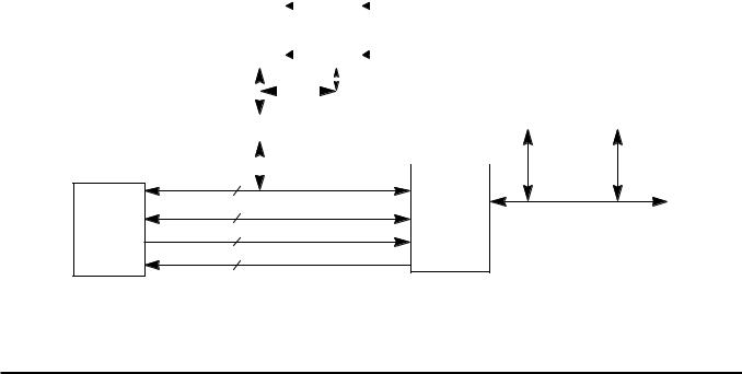
Figure 4 shows a typical system using the R4640. In |
the R4640. Again, the system designer has the flexibility |
||||||||||||||||||
this example two banks of DRAMs are used to supply and |
to make these price/performance trade-offs. |
||||||||||||||||||
accept data with a DDxxDD data pattern. |
|
|
|
|
|
|
System Command Bus |
|
|
|
|||||||||
The R4640 clocking interface allows the CPU to be |
|
|
|
||||||||||||||||
The R4640 interface has a 9-bit System Command |
|||||||||||||||||||
easily mated with external reference clocks. The CPU |
|||||||||||||||||||
(SysCmd) bus. The command bus indicates whether the |
|||||||||||||||||||
input clock is the bus reference clock, and can be |
|||||||||||||||||||
SysAD bus carries an address or data. If the SysAD |
|||||||||||||||||||
between 25 and 67MHz (somewhat dependent on |
|||||||||||||||||||
carries an address, then the SysCmd bus also indicates |
|||||||||||||||||||
maximum pipeline speed for the CPU). |
|
|
|
|
|
|
|||||||||||||
|
|
|
|
|
|
what type of transaction is to take place (for example, a |
|||||||||||||
An on-chip phase-locked-loop generates the pipeline |
|||||||||||||||||||
read or write). If the SysAD carries data, then the SysCmd |
|||||||||||||||||||
clock from the system interface clock by multiplying it up |
|||||||||||||||||||
bus also gives information about the data (for example, |
|||||||||||||||||||
an amount selected at system reset. Supported multi- |
|||||||||||||||||||
this is the last data word transmitted, or the cache state of |
|||||||||||||||||||
pliers are values 2 through 8 inclusive, allowing systems |
|||||||||||||||||||
this data line is clean exclusive). The SysCmd bus is |
|||||||||||||||||||
to implement pipeline clocks at significantly higher |
|||||||||||||||||||
bidirectional to support both processor requests and |
|||||||||||||||||||
frequency than the system interface clock. |
|
|
|
|
|
|
|||||||||||||
|
|
|
|
|
|
external requests to the R4640. Processor requests are |
|||||||||||||
|
|
|
|
|
|
|
|
|
|
||||||||||
System Address/Data Bus |
|
|
|
|
|
|
initiated by the R4640 and responded to by an external |
||||||||||||
The 64-bit System Address Data (SysAD) bus is used |
device. External requests are issued by an external |
||||||||||||||||||
to transfer addresses and data between the R4640 and |
device and require the R4640 to respond. |
||||||||||||||||||
the rest of the system. It is protected with an 8-bit parity |
The R4640 supports single datum (one to eight byte) |
||||||||||||||||||
check bus, SysADC. When initialized for 32-bit operation, |
and 8-word block transfers on the SysAD bus. In the case |
||||||||||||||||||
SysAD can be viewed as a 32-bit multiplexed bus, with 4 |
of a single-datum transfer, the low-order 3 address bits |
||||||||||||||||||
parity check bits. |
|
|
|
|
|
|
gives the byte address of the transfer, and the SysCmd |
||||||||||||
The system interface is configurable to allow easier |
bus indicates the number of bytes being transferred. The |
||||||||||||||||||
interfacing to memory and I/O systems of varying |
choice of 32or 64-bit wide system interface dictates |
||||||||||||||||||
frequencies. The bus frequency and reference timing of |
whether a cache line block transaction requires 4 double |
||||||||||||||||||
|
|
|
|
|
|
|
|
|
|
Address |
|
|
|
||||||
|
Boot |
|
|
DRAM |
|
|
|
|
|||||||||||
|
|
|
|
|
|
|
|
|
|
|
|
|
|||||||
|
ROM |
|
|
(80ns) |
|
Control |
|
|
|
|
|
|
|||||||
|
|
|
|
|
|
|
|
|
|
|
|
|
|
|
|
||||
|
|
|
|
|
|
|
|
|
|
|
|
|
|
|
|
|
|
|
|
|
|
|
|
|
|
|
|
|
|
|
|
|
|
|
|
|
|
|
|
|
|
|
|
|
|
|
|
|
|
|
|
|
|
|
SCSI |
|
ENET |
|
|
|
|
|
|
|
|
|
|
|
|
|
|
|
|
|
|
|
|||
|
|
|
|
|
|
|
|
|
|
|
|
|
|
|
|
|
|||
|
|
|
|
|
|
|
|
|
|
|
|
|
|
|
|
|
|||
|
|
|
|
|
|
|
|
|
|
|
|
|
|
|
|
|
|
||
|
|
|
|
|
|
|
|
|
|
|
|
|
|
|
|
|
|
|
|
|
|
|
|
|
|
|
|
|
|
|
|
|
|
|
|
|
|
|
|
|
|
|
|
|
|
|
|
|
|
|
|
|
|
|
|
|
|
|
|
|
|
|
|
|
|
|
|
|
|
|
|
|
|
|
|
|
|
|
|
|
|
|
|
|
|
|
|
|
|
|
|
|
|
|
|
|
|
|
|
|
|
|
|
|
|
|
|
|
|
|
|
|
|
|
|
|
|
|
|
32 |
Memory I/O |
|
Controller |
||
|
RV4640 |
9 |
|
2 |
|
11 |
Figure 4: Typical R4640 System Architecture
7
 Loading...