


Integrated Device Technology Inc IDT7132LA35FB, IDT7132LA35J, IDT7132LA35JB, IDT7132LA35L48B, IDT7132LA35P Datasheet
...
|
|
|
|
|
|
|
|
|
HIGH-SPEED |
IDT7132SA/LA |
|
|
|
|
|
|
|
|
|
2K x 8 DUAL-PORT |
IDT7142SA/LA |
|
|
|
|
|
|
|
|
|
||
|
|
|
|
|
|
|
|
|
||
|
|
|
|
|
|
|
|
|
STATIC RAM |
|
Integrated Device Technology, Inc. |
|
|
|
|||||||
|
|
|
|
|
|
|
|
|
|
|
|
|
|
|
|
|
|
|
|
|
|
FEATURES:
•High-speed access
—Military: 25/35/55/100ns (max.)
—Commercial: 25/35/55/100ns (max.)
—Commercial: 20ns only in PLCC for 7132
•Low-power operation
—IDT7132/42SA
Active: 550mW (typ.) Standby: 5mW (typ.)
— IDT7132/42LA Active: 550mW (typ.) Standby: 1mW (typ.)
•Fully asynchronous operation from either port
•MASTER IDT7132 easily expands data bus width to 16-or- more bits using SLAVE IDT7142
•On-chip port arbitration logic (IDT7132 only)
•BUSY output flag on IDT7132; BUSY input on IDT7142
•Battery backup operation —2V data retention
•TTL-compatible, single 5V ±10% power supply
•Available in popular hermetic and plastic packages
•Military product compliant to MIL-STD, Class B
•Standard Military Drawing # 5962-87002
•Industrial temperature range (–40°C to +85°C) is available, tested to miliary electrical specifications
DESCRIPTION:
The IDT7132/IDT7142 are high-speed 2K x 8 Dual-Port Static RAMs. The IDT7132 is designed to be used as a standalone 8-bit Dual-Port RAM or as a “MASTER” Dual-Port RAM together with the IDT7142 “SLAVE” Dual-Port in 16-bit-or- more word width systems. Using the IDT MASTER/SLAVE Dual-Port RAM approach in 16-or-more-bit memory system applications results in full-speed, error-free operation without the need for additional discrete logic.
Both devices provide two independent ports with separate control, address, and l/O pins that permit independent, asynchronous access for reads or writes to any location in memory. An automatic power down feature, controlled by CE permits the on-chip circuitry of each port to enter a very low standby power mode.
Fabricated using IDT’s CMOS high-performance technology, these devices typically operate on only 550mW of power. Low-power (LA) versions offer battery backup data retention capability, with each Dual-Port typically consuming 200μW from a 2V battery.
The IDT7132/7142 devices are packaged in a 48-pin sidebraze or plastic DIPs, 48-pin LCCs, 52-pin PLCCs, and 48-lead flatpacks. Military grade product is manufactured in compliance with the latest revision of MIL-STD-883, Class B, making it ideally suited to military temperature applications demanding the highest level of performance and reliability.
FUNCTIONAL BLOCK DIAGRAM
OEL
CEL
R/WL
I/O0L- I/O7L 
(1,2)
BUSYL
A10L
A0L
NOTES:
1.IDT7132 (MASTER): BUSY is open
drain output and requires pullup resistor of 270Ω.
IDT7142 (SLAVE): BUSY is input.
2.Open drain output: requires pullup resistor of 270Ω.
OER
CER
R/WR
I/O |
|
I/O |
I/O0R-I/O7R |
|
|
||
Control |
|
Control |
|
|
|
|
(1,2) |
|
|
|
BUSYR |
Address |
MEMORY |
Address |
A10R |
|
|||
Decoder |
ARRAY |
Decoder |
A0R |
|
|
|
|
11 |
|
11 |
|
|
|
|
|
|
ARBITRATION |
|
|
CEL |
LOGIC |
CER |
|
|
|
||
|
|
|
2692 drw 01 |
The IDT logo is a registered trademark of Integrated Device Technology, Inc.
MILITARY AND COMMERCIAL TEMPERATURE RANGES |
OCTOBER 1996 |
©1996 Integrated Device Technology, Inc. For latest information contact IDT’s web site at www.idt.com or fax-on-demand at 408-492-8391. |
DSC-2692/8 |
6.02 |
1 |
IDT7132SA/LA AND IDT7142SA/LA
HIGH-SPEED 2K x 8 DUAL-PORT STATIC RAM
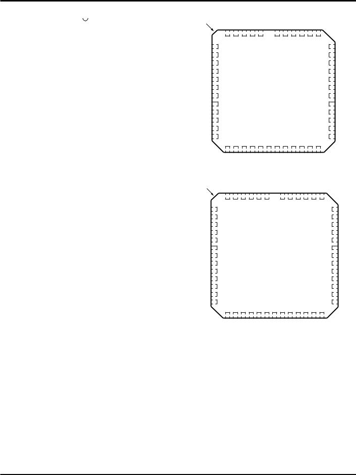
PIN CONFIGURATIONS (1,2)
CEL |
|
1 |
|
48 |
|
VCC |
|
|
|
||||
|
|
|
||||
R/WL |
|
2 |
|
47 |
|
CER |
|
|
|
||||
BUSYL |
|
3 |
|
46 |
|
R/WR |
|
|
|
||||
A10L |
|
4 |
|
45 |
|
BUSYR |
|
|
|
||||
OEL |
|
5 |
|
44 |
|
A10R |
|
|
|
||||
A0L |
|
6 |
|
43 |
|
OER |
|
|
|
||||
A1L |
|
7 |
|
42 |
|
A0R |
|
|
|
||||
A2L |
|
8 |
IDT7132/ |
41 |
|
A1R |
|
|
|||||
A3L |
|
9 |
40 |
|
A2R |
|
|
7142 |
|
||||
A4L |
|
10 |
39 |
|
A3R |
|
|
|
|
||||
A5L |
|
11 |
P48-1 |
38 |
|
A4R |
|
|
|||||
A6L |
|
12 |
37 |
|
A5R |
|
|
& |
|
||||
A7L |
|
13 |
36 |
|
A6R |
|
|
C48-2 |
|
||||
|
|
|||||
A8L |
|
14 |
|
35 |
|
A7R |
|
|
|
||||
A9L |
|
15 |
DIP |
34 |
|
A8R |
|
|
|||||
I/O0L |
|
16 |
TOP |
33 |
|
A9R |
|
|
|||||
I/O1L |
|
17 VIEW (3) |
32 |
|
I/O7R |
|
|
|
|||||
I/O2L |
|
18 |
|
31 |
|
I/O6R |
|
|
|
||||
I/O3L |
|
19 |
|
30 |
|
I/O5R |
|
|
|
||||
I/O4L |
|
20 |
|
29 |
|
I/O4R |
|
|
|
||||
I/O5L |
|
21 |
|
28 |
|
I/O3R |
|
|
|
||||
I/O6L |
|
22 |
|
27 |
|
I/O2R |
|
|
|
||||
I/O7L |
|
23 |
|
26 |
|
I/O1R |
|
|
|
||||
GND |
|
24 |
|
25 |
|
I/O0R |
|
|
|
||||
2692 drw 02
NOTES:
1.All Vcc pins must be connected to the power supply.
2.All GND pins must be connected to the ground supply.
3.This text does not indicate orientation of the actual part-marking.
ABSOLUTE MAXIMUM RATINGS(1)
Symbol |
Rating |
Commercial |
Military |
Unit |
|
|
|
|
|
|
|
VTERM(2) |
Terminal Voltage |
-0.5 to +7.0 |
-0.5 to +7.0 |
V |
|
|
with Respect to |
|
|
|
|
|
GND |
|
|
|
|
TA |
Operating |
0 to +70 |
-55 to +125 |
°C |
|
|
Temperature |
|
|
|
|
TBIAS |
Temperature |
-55 to +125 |
-65 to +135 |
°C |
|
|
Under Bias |
|
|
|
|
TSTG |
Storage |
-55 to +125 |
-65 to +150 |
°C |
|
|
Temperature |
|
|
|
|
IOUT |
DC Output |
50 |
50 |
mA |
|
|
Current |
|
|
|
|
|
|
|
|
|
|
NOTES: |
|
|
|
2692 tbl 01 |
|
1.Stresses greater than those listed under ABSOLUTE MAXIMUM RATINGS may cause permanent damage to the device. This is a stress rating only and functional operation of the device at these or any other conditions above those indicated in the operational sections of the specification is not implied. Exposure to absolute maximum rating conditions for extended periods may affect reliability.
2.VTERM must not exceed Vcc + 0.5V for more than 25% of the cycle time or 10ns maximum, and is limited to < 20mA for the period of VTERM > Vcc + 0.5V.
RECOMMENDED OPERATING TEMPERATURE AND SUPPLY VOLTAGE
|
Ambient |
|
|
Grade |
Temperature |
GND |
VCC |
|
|
|
|
Military |
-55°C to +125°C |
0V |
5.0V ± 10% |
Commercial |
0°C to +70°C |
0V |
5.0V ± 10% |
2692 tbl 02
MILITARY AND COMMERCIAL TEMPERATURE RANGES
INDEX |
|
|
|
A0L |
OEL |
A10L |
BUSYL |
R/WL |
CEL VCC |
CER R/WR |
BUSY R A10R |
OER |
|
|||||
|
|
|
|
6 |
5 |
4 |
3 |
2 |
|
|
48 47 46 45 44 43 |
|
||||||
|
|
|
|
1 |
A0R |
|||||||||||||
A1L |
7 |
|
|
|
|
|
|
|
|
|
|
42 |
||||||
A2L |
8 |
|
|
|
|
|
|
|
|
|
|
|
|
41 |
A1R |
|||
A3L |
9 |
|
|
|
|
|
|
|
|
|
|
|
|
40 |
A2R |
|||
A4L |
10 |
|
|
|
IDT7132/42 |
|
|
39 |
A3R |
|||||||||
|
|
|
|
|
|
|
|
|
|
|
A4R |
|||||||
A5L |
11 |
|
|
|
|
|
L48-1 |
|
|
38 |
||||||||
A6L |
12 |
|
|
|
|
|
|
& |
|
|
|
37 |
A5R |
|||||
|
|
|
|
|
F48-1 |
|
|
|||||||||||
A7L |
13 |
|
48-PIN LCC/ FLATPACK |
|
36 |
A6R |
||||||||||||
A8L |
14 |
|
|
35 |
A7R |
|||||||||||||
|
|
|
TOP VIEW (3) |
|
|
|||||||||||||
A9L |
15 |
|
|
|
|
|
|
|
|
|
|
|
|
34 |
A8R |
|||
I/O0L |
16 |
|
|
|
|
|
|
|
|
|
|
|
|
33 |
A9R |
|||
I/O1L |
17 |
|
|
|
|
|
|
|
|
|
|
|
|
32 |
I/O7R |
|||
I/O2L |
18 |
|
|
|
|
|
|
|
|
|
|
|
|
31 |
I/O6R |
|||
|
|
|
|
19 20 21 22 23 24 25 26 27 28 29 30 |
|
|||||||||||||
|
|
|
|
I/O3L |
I/O4L |
I/O5L |
6LI/O |
7LI/O |
|
GND |
|
0RI/O |
I/O1R I/O2R |
I/O3R |
I/O4R |
I/O5R |
2692 drw 03 |
|
|
|
|
|
|
|
|
|
|
|
|
|
|
|
|
|
|
|
|
|
|
|
|
|
|
|
|
L |
|
|
|
|
|
|
R |
|
|
|
INDEX |
|
|
A0L |
OEL |
A10L |
N/C |
BUSY |
R/WL |
LCE |
VCC CER R/WR BUSY |
N/C A10R |
|
||||||
|
|
|
|
|
|
|||||||||||||
|
|
|
|
7 |
6 |
5 |
4 |
3 |
2 |
|
|
|
52 51 50 49 48 47 |
|
||||
|
|
|
|
|
|
|
|
|||||||||||
A1L |
8 |
|
|
1 |
|
|
|
46 |
OER |
A2L |
9 |
|
|
|
|
|
|
45 |
A0R |
A3L |
10 |
|
|
|
|
|
|
44 |
A1R |
A4L |
11 |
|
|
IDT7132/42 |
|
|
|
43 |
A2R |
A5L |
12 |
|
|
|
|
|
42 |
A3R |
|
|
|
J52-1 |
|
|
|
||||
A6L |
13 |
|
|
52-PIN PLCC |
|
|
|
41 |
A4R |
A7L |
14 |
|
|
|
|
|
40 |
A5R |
|
|
|
TOP VIEW (3) |
|
|
|
||||
A8L |
15 |
|
|
|
|
|
|
39 |
A6R |
A9L |
16 |
|
|
|
|
|
|
38 |
A7R |
I/O0L |
17 |
|
|
|
|
|
|
37 |
A8R |
I/O1L |
18 |
|
|
|
|
|
|
36 |
A9R |
I/O2L |
19 |
|
|
|
|
|
|
35 |
N/C |
I/O3L |
20 |
|
|
|
|
|
|
34 |
I/O7R |
|
21 22 23 24 25 26 27 28 29 30 31 32 33 |
|
|||||||
|
I/O4L |
I/O5L I/O6L |
I/O7L |
N/C GND I/O0R I/O1R I/O2R |
I/O3R |
I/O4R |
I/O5R |
I/O6R |
2692 drw 04 |
|
|
||||||||
NOTES:
1.All Vcc pins must be connected to the power supply.
2.All GND pins must be connected to the ground supply.
3.This text does not indicate orientation of the actual part-marking.
RECOMMENDED
DC OPERATING CONDITIONS
Symbol |
Parameter |
Min. |
Typ. |
Max. |
Unit |
VCC |
Supply Voltage |
4.5 |
5.0 |
5.5 |
V |
|
|
|
|
|
|
GND |
Supply Voltage |
0 |
0 |
0 |
V |
|
|
|
|
|
|
VIH |
Input High Voltage |
2.2 |
— |
6.0(2) |
V |
VIL |
Input Low Voltage |
-0.5(1) |
— |
0.8 |
V |
NOTES: |
2692 tbl 03 |
|
1.VIL (min.) = -1.5V for pulse width less than 10ns.
2.VTERM must not exceed Vcc + 0.5V.
6.02 |
2 |

IDT7132SA/LA AND IDT7142SA/LA |
|
HIGH-SPEED 2K x 8 DUAL-PORT STATIC RAM |
MILITARY AND COMMERCIAL TEMPERATURE RANGES |
DC ELECTRICAL CHARACTERISTICS OVER THE
OPERATING TEMPERATURE AND SUPPLY VOLTAGE RANGE(1,6) (VCC = 5.0V ± 10%)
|
|
|
|
|
7132X20(2) |
7132X25(3) |
7132X35 |
7132X55 |
7132X100 |
|
|||||
|
|
|
|
|
|
|
7142X25(3) |
7142X35 |
7142X55 |
7142X100 |
|
||||
Symbol |
Parameter |
Test Conditions |
Version |
Typ. Max. |
Typ. Max. |
Typ. Max. |
Typ. Max. |
Typ. Max. |
Unit |
||||||
|
|
|
|
|
|
|
|
|
|
|
|
|
|
|
|
ICC |
Dynamic Operating |
CEL and CER = VIL, |
MIL. |
SA |
— |
— |
110 |
280 |
80 |
230 |
65 |
190 |
65 |
190 |
mA |
|
Current (Both Ports |
Outputs open, |
|
LA |
— |
— |
110 |
220 |
80 |
170 |
65 |
140 |
65 |
140 |
|
|
Active) |
f = fMAX(4) |
COM'L. SA |
110 |
250 |
110 |
220 |
80 |
165 |
65 |
155 |
65 |
155 |
|
|
|
|
|
|
LA |
110 |
200 |
110 |
170 |
80 |
120 |
65 |
110 |
65 |
110 |
|
|
|
|
|
|
|
|
|
|
|
|
|
|
|
|
|
ISB1 |
Standby Current |
CEL and CER = VIH, |
MIL. |
SA |
— |
— |
30 |
80 |
25 |
80 |
20 |
65 |
20 |
65 |
mA |
|
(Both Ports - TTL |
f = fMAX(4) |
|
LA |
— |
— |
30 |
60 |
25 |
60 |
20 |
45 |
20 |
45 |
|
|
Level Inputs) |
|
COM'L. SA |
30 |
65 |
30 |
65 |
25 |
65 |
20 |
65 |
20 |
55 |
|
|
|
|
|
|
LA |
30 |
45 |
30 |
45 |
25 |
45 |
20 |
35 |
20 |
35 |
|
|
|
|
|
|
|
|
|
|
|
|
|
|
|
|
|
ISB2 |
Standby Current |
CE"A" = VIL and |
MIL. |
SA |
— |
— |
65 |
160 |
50 |
150 |
40 |
125 |
40 |
125 |
mA |
|
(One Port - TTL |
CE"B" = VIH (7) |
|
LA |
— |
— |
65 |
125 |
50 |
115 |
40 |
90 |
40 |
90 |
|
|
Level Inputs) |
Active Port Outputs |
COM'L. SA |
65 |
165 |
65 |
150 |
50 |
125 |
40 |
110 |
40 |
110 |
|
|
|
|
Open, f = fMAX(4) |
|
LA |
65 |
125 |
65 |
115 |
50 |
90 |
40 |
75 |
40 |
75 |
|
ISB3 |
Full Standby Current |
CEL and |
MIL. |
SA |
— |
— |
1.0 |
30 |
1.0 |
30 |
1.0 |
30 |
1.0 |
30 |
mA |
|
(Both Ports - All |
CER > VCC -0.2V, |
|
LA |
— |
— |
0.2 |
10 |
0.2 |
10 |
0.2 |
10 |
0.2 |
10 |
|
|
CMOS Level Inputs |
VIN > VCC -0.2V or |
COM'L. SA |
1.0 |
15 |
1.0 |
15 |
1.0 |
15 |
1.0 |
15 |
1.0 |
15 |
|
|
|
|
VIN < 0.2V,f = 0(5) |
|
LA |
0.2 |
5 |
0.2 |
5 |
0.2 |
4 |
0.2 |
4 |
0.2 |
4 |
|
ISB4 |
Full Standby Current |
CE"A" < 0.2V and |
MIL. |
SA |
— |
— |
60 |
155 |
45 |
145 |
40 |
110 |
40 |
110 |
mA |
|
(One Port - All |
CE"B" > VCC -0.2V(7) |
|
LA |
— |
— |
60 |
115 |
45 |
105 |
40 |
85 |
40 |
80 |
|
|
CMOS Level Inputs) |
VIN > VCC -0.2V or |
COM'L. SA |
60 |
155 |
60 |
145 |
45 |
110 |
40 |
100 |
40 |
95 |
|
|
|
|
VIN < 0.2V, |
|
LA |
60 |
115 |
60 |
105 |
45 |
85 |
40 |
70 |
40 |
70 |
|
|
|
Active Port Outputs |
|
|
|
|
|
|
|
|
|
|
|
|
|
|
|
Open, f = fMAX(4) |
|
|
|
|
|
|
|
|
|
|
|
|
|
NOTES: |
|
|
|
|
|
|
|
|
|
|
|
|
|
2689 tbl 04 |
|
1.'X' in part numbers indicates power rating (SA or LA).
2.Com'l Only, 0°C to +70°C temperature range. PLCC package only.
3.Not available in DIP packages.
4.At f = fMax, address and control lines (except Output Enable) are cycling at the maximum frequency read cycle of 1/tRC, and using “AC TEST CONDITIONS” of input levels of GND to 3V.
5.f = 0 means no address or control lines change. Applies only to inputs at CMOS level standby.
6.Vcc = 5V, TA=+25°C for Typ. and is not production tested. Vcc DC = 100mA (Typ.)
7.Port "A" may be either left or right port. Port "B" is opposite from port "A".
DC ELECTRICAL CHARACTERISTICS OVER THE
OPERATING TEMPERATURE AND SUPPLY VOLTAGE RANGE (VCC = 5.0V ± 10%)
|
|
|
7132SA |
|
7132LA |
|
|
|
|
|
7142SA |
|
7142LA |
|
|
Symbol |
Parameter |
Test Conditions |
Min. |
Max. |
Max. |
Max. |
Unit |
|
|
|
|
|
|
|
|
|lLl| |
Input Leakage |
VCC = 5.5V, |
— |
10 |
— |
5 |
μA |
|
Current(1) |
VIN = 0V to VCC |
|
|
|
|
|
|lLO| |
Output Leakage |
VCC = 5.5V, |
— |
10 |
— |
5 |
μA |
|
Current(1) |
CE = VIH, VOUT = 0V to VCC |
|
|
|
|
|
VOL |
Output Low Voltage |
lOL = 4mA |
— |
0.4 |
— |
0.4 |
V |
|
(l/O0-l/O7) |
|
|
|
|
|
|
|
|
|
|
|
|
|
|
VOL |
Open Drain Output |
lOL = 16mA |
— |
0.5 |
— |
0.5 |
V |
|
Low Voltage (BUSY, INT) |
|
|
|
|
|
|
|
|
|
|
|
|
|
|
VOH |
Output High Voltage |
lOH = -4mA |
2.4 |
— |
2.4 |
— |
V |
|
|
|
|
|
|
|
|
NOTE: |
|
|
|
|
|
|
2689 tbl 05 |
1. At Vcc < 2.0V leakages are undefined.
6.02 |
3 |
IDT7132SA/LA AND IDT7142SA/LA |
|
HIGH-SPEED 2K x 8 DUAL-PORT STATIC RAM |
MILITARY AND COMMERCIAL TEMPERATURE RANGES |
DATA RETENTION CHARACTERISTICS (LA Version Only)
|
|
|
|
lDT7132LA/IDT7142LA |
|
||
Symbol |
Parameter |
Test Conditions |
|
Min. |
Typ. |
Max. |
Unit |
|
|
|
|
|
|
|
|
VDR |
VCC for Data Retention |
|
|
2.0 |
— |
— |
V |
|
|
|
|
|
|
|
|
ICCDR |
Data Retention Current |
VCC = 2.0V, CE ³ VCC -0.2V |
Mil. |
— |
100 |
4000 |
mA |
|
|
VIN ³ VCC -0.2V or VIN £ 0.2V |
|
|
|
|
|
|
|
Com’l. |
— |
100 |
1500 |
mA |
|
|
|
|
|
|
|
|
|
(3) |
Chip Deselect to Data |
|
|
0 |
— |
— |
ns |
tCDR |
|
|
|||||
|
Retention Time |
|
|
|
|
|
|
|
|
|
|
|
|
|
|
tR(3) |
Operation Recovery |
|
|
tRC(2) |
— |
— |
ns |
|
Time |
|
|
|
|
|
|
NOTES: |
|
|
|
|
|
|
2692 tbl 06 |
1.VCC = 2V, TA = +25°C, and is not production tested.
2.tRC = Read Cycle Time
3.This parameter is guaranteed but not production tested.
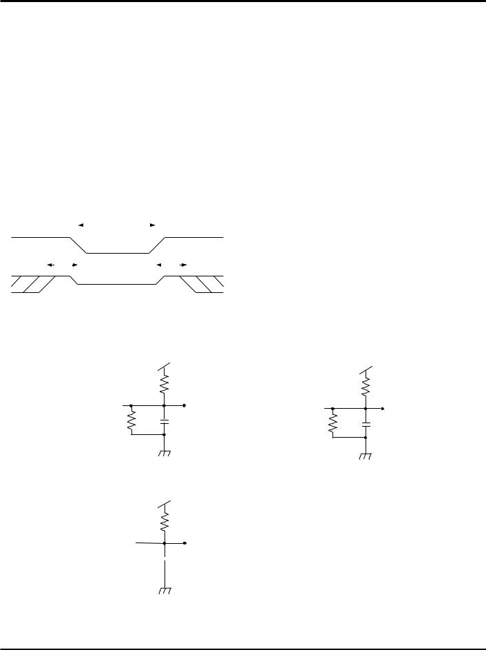
DATA RETENTION WAVEFORM |
|
|
|
|
|
|
AC TEST CONDITIONS |
|
||||||||||||||
|
|
|
|
DATA RETENTION MODE |
|
|
|
|
|
|
Input Pulse Levels |
GND TO 3.0V |
||||||||||
|
|
|
|
|
|
|
|
|
|
Input Rise/Fall Times |
5ns |
|||||||||||
|
|
|
|
|
|
|
|
|
|
|
|
|
|
|
|
|
|
|
|
|
Input Timing Reference Levels |
1.5V |
|
|
|
|
|
|
|
|
|
|
|
|
|
|
|
|
|
|
|
|
|
||
VCC |
|
|
|
|
|
|
|
|
VDR ³2.0V |
|
|
|
|
|
|
|
|
|
|
Output Reference Levels |
1.5V |
|
|
|
|
4.5V |
|
|
|
|
|
4.5V |
|
Output Load |
Figures 1, 2, and 3 |
||||||||||
|
|
|
|
|
|
|
|
|||||||||||||||
|
|
|
|
|
|
|
|
|
|
|
|
|
|
|||||||||
|
|
|
|
|
|
|
|
|
|
|
|
|
|
|
|
|
|
|
|
|
|
|
|
|
|
|
|
|
|
|
|
|
|
|
|
|
|
|
|
|
|
|
|
|
2692 tbl 07 |
CE |
|
|
|
tCDR |
|
|
|
|
VDR |
|
|
|
|
tR |
|
|
|
|
|
|
||
|
|
|
|
|
|
|
|
|
|
|
|
|
|
|
|
|
|
|
|
|||
|
|
|
|
|
|
|
|
|
|
|
|
|
|
|
|
|
|
|
|
|
|
|
|
|
VIH |
|
|
|
|
|
|
|
|
|
VIH |
|
|
2692 drw 05 |
|
||||||
|
|
|
|
|
|
|
|
|
|
|
|
|
|
|
||||||||
|
|
|
|
|
|
|
|
|
|
|
|
|
|
|||||||||
|
|
|
|
|
|
|
|
|
|
|
|
|
|
|
|
|
|
|
|
|
||
|
5V |
|
5V |
|
|
|
|
||
|
1250Ω |
|
1250Ω |
|
|
|
|
||
DATA OUT |
|
DATA OUT |
|
|
775Ω |
|
|
||
30pF* |
775Ω |
5pF* |
||
|
||||
|
100pF for 55 and 100ns versions |
|
|
|
|
|
|
2692 drw 06 |
|
Figure 1. AC Output Test Load |
Figure 2. Output Test Load |
|||
|
|
|
(for tHZ, tLZ, tWZ, and tOW) |
|
5V |
* Including scope and jig |
|
270Ω
BUSY or INT
 30pF*
30pF*
100pF for 55 and 100ns versions
Figure 3. BUSY and INT
AC Output Test Load
6.02 |
4 |
 Loading...