


Integrated Device Technology Inc IDT70V24L25G, IDT70V24L25J, IDT70V24L25PF, IDT70V24L35G, IDT70V24L35J Datasheet
...
HIGH-SPEED 3.3V |
IDT70V24S/L |
4K x 16 DUAL-PORT |
|
STATIC RAM |
|
Integrated Device Technology, Inc.
FEATURES:
•True Dual-Ported memory cells which allow simultaneous access of the same memory location
•High-speed access
—Commercial: 25/35/55ns (max.)
•Low-power operation
—IDT70V24S
Active: 230mW (typ.) Standby: 3.3mW (typ.)
—IDT70V24L
Active: 230mW (typ.) Standby: .66mW (typ.)
•Separate upper-byte and lower-byte control for multiplexed bus compatibility
•IDT70V24 easily expands data bus width to 32 bits or more using the Master/Slave select when cascading more than one device
•M/S = H for BUSY output flag on Master M/S = L for BUSY input on Slave
•Busy and Interrupt Flags
•Devices are capable of withstanding greater than 2001V electrostatic charge.
•On-chip port arbitration logic
•Full on-chip hardware support of semaphore signaling between ports
•Fully asynchronous operation from either port
•LVTTL-compatible, single 3.3V (±0.3V) power supply
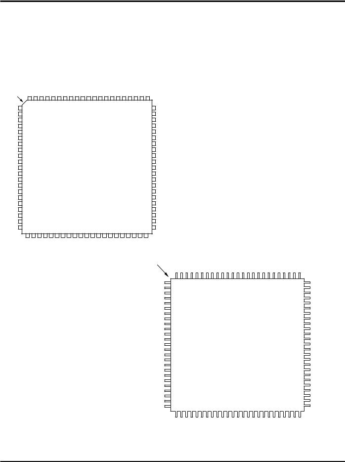
•Available in 84-pin PGA, 84-pin PLCC, and 100-pin TQFP
DESCRIPTION:
The IDT70V24 is a high-speed 4K x 16 Dual-Port Static RAM. The IDT70V24 is designed to be used as a stand-alone 64K-bit Dual-Port RAM or as a combination MASTER/SLAVE
FUNCTIONAL BLOCK DIAGRAM
R/WL |
R/WR |
UBL |
UBR |
LBL |
LBR |
CEL |
CER |
OEL |
OER |
I/O8L-I/O15L |
I/O8R-I/O15R |
I/O |
I/O |
Control |
Control |
I/O0L-I/O7L |
I/O0R-I/O7R |
(1,2)
BUSYL
NOTES:
1.(MASTER): BUSY is output; (SLAVE): BUSY is input.
2.BUSY outputs and INT outputs are non-tri-stated push-pull.
A11L 
A0L 
SEML 
(2)
INTL
|
|
|
BUSYR(1,2) |
Address |
MEMORY |
Address |
A11R |
|
|||
Decoder |
ARRAY |
Decoder |
A0R |
|
|
|
|
|
1 2 |
1 2 |
|
|
|
|
|
|
ARBITRATION |
|
|
CEL |
INTERRUPT |
CER |
|
SEMAPHORE |
|
||
OEL |
OER |
|
|
LOGIC |
|
||
R/WL |
R/WR |
|
|
|
|
||
|
|
|
SEMR |
|
M/S |
|
INTR(2) |
|
|
2911 drw 01 |
The IDT logo is a registered trademark of Integrated Device Technology, Inc.
COMMERCIAL TEMPERATURE RANGE |
OCTOBER 1996 |
|
©1996 Integrated Device Technology, Inc. |
For latest information contact IDT’s web site at www.idt.com or fax-on-demand at 408-492-8391. |
DSC-2911/3 |
|
6.38 |
1 |
IDT70V24S/L |
|
HIGH-SPEED 3.3V 4K x 16 DUAL-PORT STATIC RAM |
COMMERCIAL TEMPERATURE RANGE |
Dual-Port RAM for 32-bit-or-more word systems. Using the IDT MASTER/SLAVE Dual-Port RAM approach in 32-bit or wider memory system applications results in full-speed, errorfree operation without the need for additional discrete logic.
This device provides two independent ports with separate control, address, and I/O pins that permit independent, asynchronous access for reads or writes to any location in
memory. An automatic power down feature controlled by CE permits the on-chip circuitry of each port to enter a very low standby power mode.
Fabricated using IDT’s CMOS high-performance technology, these devices typically operate on only 350mW of power.
The IDT70V24 is packaged in a ceramic 84-pin PGA, an 84-Pin PLCC, and a 100-pin Thin Quad Plastic Flatpack.
PIN CONFIGURATIONS (1,2)
INDEX |
I/O7L |
I/O6L |
I/O5L |
I/O4L |
I/O3L |
I/O2L |
GND |
I/O1L |
I/O0L |
OEL |
VCC R/WL SEML |
CEL |
UBL |
LBL N/C |
A11L |
A10L |
A9L |
A8L |
|
|
|
|
|
|
|
|
|
|
|
|
|
|
|
|
|
|
|
|
|
|
|
I/O8L |
11 10 |
9 |
8 |
7 |
6 |
5 |
4 |
3 |
2 |
1 84 83 82 81 80 79 78 77 76 75 |
A7L |
|
|
|
|
|
|
|
|
|
|
|
|
|
|
|
|
|
|
|
|
|
|
||||||||
12 |
|
|
|
|
|
|
|
|
|
|
|
|
|
|
|
|
74 |
|
|
|
|
|
|
|
|
|
|
|
|
|
|
|
|
|
|
|
|
|
|
||
I/O9L |
13 |
|
|
|
|
|
|
|
|
|
|
|
|
|
|
|
|
73 |
A6L |
|
|
|
|
|
|
|
|
|
|
|
|
|
|
|
|
|
|
|
|
|
|
I/O10L |
14 |
|
|
|
|
|
|
|
|
|
|
|
|
|
|
|
|
72 |
A5L |
|
|
|
|
|
|
|
|
|
|
|
|
|
|
|
|
|
|
|
|
|
|
I/O11L |
15 |
|
|
|
|
|
|
|
|
|
|
|
|
|
|
|
|
71 |
A4L |
|
|
|
|
|
|
|
|
|
|
|
|
|
|
|
|
|
|
|
|
|
|
I/O12L |
16 |
|
|
|
|
|
|
|
|
|
|
|
|
|
|
|
|
70 |
A3L |
|
|
|
|
|
|
|
|
|
|
|
|
|
|
|
|
|
|
|
|
|
|
I/O13L |
17 |
|
|
|
|
|
|
|
|
|
|
|
|
|
|
|
|
69 |
A2L |
|
|
|
|
|
|
|
|
|
|
|
|
|
|
|
|
|
|
|
|
|
|
GND |
18 |
|
|
|
|
|
|
|
|
|
|
|
|
|
|
|
|
68 |
A1L |
|
|
|
|
|
|
|
|
|
|
|
|
|
|
|
|
|
|
|
|
|
|
|
|
|
|
|
|
|
IDT70V24 |
|
|
|
|
|
|
A0L |
|
|
|
|
|
|
|
|
|
|
|
|
|
|
|
|
|
|
|
|
|
|
|||||
I/O14L |
19 |
|
|
|
|
|
|
|
|
|
|
|
|
|
67 |
|
|
|
|
|
|
|
|
|
|
|
|
|
|
|
|
|
|
|
|
|
|
||||
|
|
|
|
|
|
|
|
J84-1 |
|
|
|
|
|
|
|
|
|
|
|
|
|
|
|
|
|
|
|
|
|
|
|
|
|
|
|
|
|
||||
I/O15L |
|
|
|
|
|
|
|
|
|
|
|
|
|
|
|
66 |
INTL |
|
|
|
|
|
|
|
|
|
|
|
|
|
|
|
|
|
|
|
|
|
|
||
20 |
|
|
|
|
|
|
|
|
F84-2 |
|
|
|
|
|
|
|
|
|
|
|
|
|
|
|
|
|
|
|
|
|
|
|
|
|
|
|
|
||||
|
|
|
|
|
|
|
|
|
|
|
|
|
|
|
|
|
|
|
|
|
|
|
|
|
|
|
|
|
|
|
|
|
|
|
|
|
|||||
VCC |
21 |
|
|
|
|
|
|
|
84-PIN PLCC/ |
|
|
|
|
|
|
65 |
BUSYL |
|
|
|
|
|
|
|
|
|
|
|
|
|
|
|
|
|
|
|
|
|
|
||
GND |
22 |
|
|
|
|
|
|
|
|
|
|
|
|
|
64 |
GND |
|
|
|
|
|
|
|
|
|
|
|
|
|
|
|
|
|
|
|
|
|
|
|||
|
|
|
|
|
|
|
FLATPACK |
|
|
|
|
|
|
|
|
|
|
|
|
|
|
|
|
|
|
|
|
|
|
|
|
|
|
|
|
||||||
I/O0R |
23 |
|
|
|
|
|
|
|
TOP VIEW (3) |
|
|
|
|
|
|
63 |
M/S |
|
|
|
|
|
|
|
|
|
|
|
|
|
|
|
|
|
|
|
|
|
|
||
I/O1R |
24 |
|
|
|
|
|
|
|
|
|
|
|
|
|
|
|
|
62 |
BUSYR |
|
|
|
|
|
|
|
|
|
|
|
|
|
|
|
|
|
|
|
|
|
|
I/O2R |
25 |
|
|
|
|
|
|
|
|
|
|
|
|
|
|
|
|
61 |
INTR |
|
|
|
|
|
|
|
|
|
|
|
|
|
|
|
|
|
|
|
|
|
|
VCC |
26 |
|
|
|
|
|
|
|
|
|
|
|
|
|
|
|
|
60 |
A0R |
|
|
|
|
|
|
|
|
|
|
|
|
|
|
|
|
|
|
|
|
|
|
I/O3R |
27 |
|
|
|
|
|
|
|
|
|
|
|
|
|
|
|
|
59 |
A1R |
|
|
|
|
|
|
|
|
|
|
|
|
|
|
|
|
|
|
|
|
|
|
I/O4R |
28 |
|
|
|
|
|
|
|
|
|
|
|
|
|
|
|
|
58 |
A2R |
|
|
|
|
|
|
|
|
|
|
|
|
|
|
|
|
|
|
|
|
|
|
I/O5R |
29 |
|
|
|
|
|
|
|
|
|
|
|
|
|
|
|
|
57 |
A3R |
|
|
|
|
|
|
|
|
|
|
|
|
|
|
|
|
|
|
|
|
|
|
I/O6R |
30 |
|
|
|
|
|
|
|
|
|
|
|
|
|
|
|
|
56 |
A4R |
|
|
|
|
|
|
|
|
|
|
|
|
|
|
|
|
|
|
|
|
|
|
I/O7R |
31 |
|
|
|
|
|
|
|
|
|
|
|
|
|
|
|
|
55 |
A5R |
|
|
|
|
|
|
|
|
|
|
|
|
|
|
|
|
|
|
|
|
|
|
I/O8R |
32 |
|
|
|
|
|
|
|
|
|
|
|
|
|
|
|
|
54 |
A6R |
|
|
|
|
|
|
|
|
|
|
|
|
|
|
|
|
|
|
|
|
|
|
|
33 34 35 36 37 38 39 40 41 42 43 44 45 46 47 48 49 50 51 52 53 |
|
|
|
|
|
|
|
|
|
|
|
|
|
|
|
|
|
|
|
|
|
|
|
|||||||||||||||||
|
I/O9R |
I/O10R |
I/O11R |
I/O12R |
I/O13R |
I/O14R |
GND |
I/O15R |
OER R/WR |
GND SEMR CER |
UBR |
LBR |
N/C A11R |
A10R |
A9R |
A8R |
A7R |
2911drw 02 |
|
|
|
|
|
|
|
|
|
|
|
|
|
|
|
|
|
|
|
|
|
||
|
|
|
|
|
|
|
|
|
|
|
|
|
|
|
|
|
|
|
|
|
|
|
|
||||||||||||||||||
|
|
|
|
|
|
|
|
|
|
|
|
|
|
|
|
|
|
|
Index |
I/O9L |
I/O8L |
I/O7L |
I/O6L |
I/O5L |
I/O4L |
I/O3L I/O2L |
GND |
I/O1L |
I/O0L OEL VCC R/WL SEML CEL UBL LBL |
N/C |
A11L |
A10L |
|
|
|
|
|
|
|||
|
|
|
|
|
|
|
|
|
|
|
|
|
|
|
|
|
|
|
|
A9L |
A8L |
A7L |
A6L |
|
|
||||||||||||||||
|
|
|
|
|
|
|
|
|
|
|
|
|
|
|
|
|
|
|
N/C |
110099 98 97 96 95 94 93 92 91 90 89 88 87 86 85 84 83 82 81 80 79 78 77 76 |
|
N/C |
|||||||||||||||||||
|
|
|
|
|
|
|
|
|
|
|
|
|
|
|
|
|
|
|
N/C |
2 |
|
|
|
|
|
|
|
|
|
|
|
|
|
|
|
|
|
|
75 |
N/C |
|
|
|
|
|
|
|
|
|
|
|
|
|
|
|
|
|
|
|
|
|
|
|
|
|
|
|
|
|
|
|
|
|
|
|
|
|
|
74 |
||||
|
|
|
|
|
|
|
|
|
|
|
|
|
|
|
|
|
|
|
N/C |
3 |
|
|
|
|
|
|
|
|
|
|
|
|
|
|
|
|
|
|
73 |
N/C |
|
|
|
|
|
|
|
|
|
|
|
|
|
|
|
|
|
|
|
|
N/C |
4 |
|
|
|
|
|
|
|
|
|
|
|
|
|
|
|
|
|
|
72 |
N/C |
|
|
|
|
|
|
|
|
|
|
|
|
|
|
|
|
|
|
|
|
I/O10L |
5 |
|
|
|
|
|
|
|
|
|
|
|
|
|
|
|
|
|
|
71 |
A5L |
|
|
|
|
|
|
|
|
|
|
|
|
|
|
|
|
|
|
|
|
I/O11L |
6 |
|
|
|
|
|
|
|
|
|
|
|
|
|
|
|
|
|
|
70 |
A4L |
|
|
|
|
|
|
|
|
|
|
|
|
|
|
|
|
|
|
|
|
I/O12L |
7 |
|
|
|
|
|
|
|
|
|
|
|
|
|
|
|
|
|
|
69 |
A3L |
|
|
|
|
|
|
|
|
|
|
|
|
|
|
|
|
|
|
|
|
I/O13L |
8 |
|
|
|
|
|
|
|
|
|
|
|
|
|
|
|
|
|
|
68 |
A2L |
|
|
|
|
|
|
|
|
|
|
|
|
|
|
|
|
|
|
|
|
GND |
9 |
|
|
|
|
|
|
|
|
|
|
|
|
|
|
|
|
|
|
67 |
A1L |
|
|
|
|
|
|
|
|
|
|
|
|
|
|
|
|
|
|
|
|
I/O14L |
10 |
|
|
|
|
|
|
|
|
IDT70V24 |
|
|
|
|
|
|
|
|
|
66 |
A0L |
|
|
|
|
|
|
|
|
|
|
|
|
|
|
|
|
|
|
|
|
I/O15L |
11 |
|
|
|
|
|
|
|
|
|
|
|
|
|
|
|
|
|
65 |
INTL |
||
|
|
|
|
|
|
|
|
|
|
|
|
|
|
|
|
|
|
|
|
|
|
|
|
|
|
|
PN100-1 |
|
|
|
|
|
|
|
|
|
|||||
|
|
|
|
|
|
|
|
|
|
|
|
|
|
|
|
|
|
|
VCC |
12 |
|
|
|
|
|
|
|
|
|
|
|
|
|
|
|
|
|
64 |
BUSYL |
||
|
|
|
|
|
|
|
|
|
|
|
|
|
|
|
|
|
|
|
|
|
|
|
|
|
|
|
|
|
|
|
|
|
|
|
|
|
|||||
|
|
|
|
|
|
|
|
|
|
|
|
|
|
|
|
|
|
|
GND |
13 |
|
|
|
|
|
|
|
|
100-PIN |
|
|
|
|
|
|
|
|
|
63 |
GND |
|
|
|
|
|
|
|
|
|
|
|
|
|
|
|
|
|
|
|
|
I/O0R |
|
|
|
|
|
|
|
|
|
|
|
|
|
|
|
|
|
|
62 |
M/S |
||
|
|
|
|
|
|
|
|
|
|
|
|
|
|
|
|
|
|
|
14 |
|
|
|
|
|
|
|
|
TQFP |
|
|
|
|
|
|
|
|
|
||||
|
|
|
|
|
|
|
|
|
|
|
|
|
|
|
|
|
|
|
I/O1R |
15 |
|
|
|
|
|
|
|
|
TOP VIEW(3) |
|
|
|
|
|
|
|
|
|
61 |
BUSYR |
|
|
|
|
|
|
|
|
|
|
|
|
|
|
|
|
|
|
|
|
I/O2R |
16 |
|
|
|
|
|
|
|
|
|
|
|
|
|
|
|
|
|
|
60 |
INTR |
|
|
|
|
|
|
|
|
|
|
|
|
|
|
|
|
|
|
|
|
VCC |
17 |
|
|
|
|
|
|
|
|
|
|
|
|
|
|
|
|
|
|
59 |
A0R |
|
|
|
|
|
|
|
|
|
|
|
|
|
|
|
|
|
|
|
|
I/O3R |
18 |
|
|
|
|
|
|
|
|
|
|
|
|
|
|
|
|
|
|
58 |
A1R |
|
|
|
|
|
|
|
|
|
|
|
|
|
|
|
|
|
|
|
|
I/O4R |
19 |
|
|
|
|
|
|
|
|
|
|
|
|
|
|
|
|
|
|
57 |
A2R |
|
|
|
|
|
|
|
|
|
|
|
|
|
|
|
|
|
|
|
|
I/O5R |
20 |
|
|
|
|
|
|
|
|
|
|
|
|
|
|
|
|
|
|
56 |
A3R |
|
|
|
|
|
|
|
|
|
|
|
|
|
|
|
|
|
|
|
|
I/O6R |
21 |
|
|
|
|
|
|
|
|
|
|
|
|
|
|
|
|
|
|
55 |
A4R |
|
|
|
|
|
|
|
|
|
|
|
|
|
|
|
|
|
|
|
|
N/C |
22 |
|
|
|
|
|
|
|
|
|
|
|
|
|
|
|
|
|
|
54 |
N/C |
|
|
|
|
|
|
|
|
|
|
|
|
|
|
|
|
|
|
|
|
N/C |
23 |
|
|
|
|
|
|
|
|
|
|
|
|
|
|
|
|
|
|
53 |
N/C |
|
|
|
|
|
|
|
|
|
|
|
|
|
|
|
|
|
|
|
|
N/C |
24 |
|
|
|
|
|
|
|
|
|
|
|
|
|
|
|
|
|
|
52 |
N/C |
|
|
|
|
|
|
|
|
|
|
|
|
|
|
|
|
|
|
|
|
N/C |
25 |
|
|
|
|
|
|
|
|
|
|
|
|
|
|
|
|
|
|
51 |
N/C |
|
|
|
|
|
|
|
|
|
|
|
|
|
|
|
|
|
|
|
|
|
26 27 28 29 30 31 32 33 34 35 36 37 38 39 40 41 42 43 44 45 46 47 48 49 50 |
|
|
|||||||||||||||||||
|
|
|
|
|
|
|
|
|
|
|
|
|
|
|
|
|
|
|
|
I/O7R |
I/O8R |
I/O9R |
I/O10R |
I/O11R |
I/O12R |
I/O13R I/O14R |
GND |
I/O15R |
ROE R/WR GND SEMR CER |
UBR |
LBR |
N/C |
A11R |
A10R |
A9R |
A8R |
A7R |
A6R |
A5R |
2911 drw 03 |
|
NOTES: |
|
|
|
|
|
|
|
|
|
|
|
|
|
|
|
|
|
|
|
|
|
||||||||||||||||||||
1.All Vcc pins must be connected to the power supply.
2.All GND pins must be connected to the ground supply.
3.This text does not indicate the actual part marking.
6.38 |
2 |

IDT70V24S/L |
|
|
|
|
|
|
|
|
|
|
|
|
|
|
|
|
|
HIGH-SPEED 3.3V 4K x 16 DUAL-PORT STATIC RAM |
|
|
|
|
|
|
|
|
|
COMMERCIAL TEMPERATURE RANGE |
|||||||
|
|
|
|
|
|
|
|
|
|
|
|
|
|
|
|
|
|
PIN CONFIGURATIONS (CONT'D)(1,2) |
|
|
|
|
|
|
|
|
|
|
|
||||||
|
|
|
|
|
|
|
|
|
|
|
|
|
|
|
|
|
|
|
63 |
61 |
60 |
|
|
58 |
55 |
|
54 |
51 |
48 |
46 |
45 |
|
|
42 |
|
11 |
I/O7L |
I/O5L |
I/O4L |
|
I/O2L |
I/O0L |
|
OEL |
SEML |
LBL |
A11L |
A10L |
|
A7L |
|
||
|
|
|
|
|
|||||||||||||
|
|
|
|
|
|
|
|
|
|
|
|
|
|
|
|
|
|
|
66 |
64 |
62 |
|
|
59 |
56 |
|
49 |
50 |
47 |
44 |
43 |
|
|
40 |
|
10 |
I/O10L |
I/O8L |
I/O6L |
|
I/O3L |
I/O1L |
|
UBL |
CEL |
N/C |
A9L |
A8L |
|
A5L |
|
||
|
|
|
|
|
|||||||||||||
|
|
|
|
|
|
|
|
|
|
|
|
|
|
|
|
|
|
|
67 |
65 |
|
|
|
|
57 |
|
53 |
52 |
|
|
41 |
|
|
39 |
|
09 |
I/O11L |
I/O9L |
|
|
|
|
GND |
|
VCC |
R/WL |
|
|
A6L |
|
A4L |
|
|
|
|
|
|
|
|
|
|
|
|
|
|
|
|
|
|
|
|
|
69 |
68 |
|
|
|
|
|
|
|
|
|
|
38 |
|
|
37 |
|
08 |
I/O13L |
I/O12L |
|
|
|
|
|
|
|
|
|
|
A3L |
|
A2L |
|
|
|
|
|
|
|
|
|
|
|
|
|
|
|
|||||
|
|
|
|
|
|
|
|
|
|
|
|
|
|
|
|
|
|
|
72 |
71 |
73 |
|
|
|
|
|
|
|
|
33 |
35 |
|
|
34 |
|
07 |
I/O15L |
I/O14L |
VCC |
|
|
|
|
|
|
|
|
BUSYL |
A0L |
|
INTL |
|
|
|
|
|
|
|
|
|
|
|
|
||||||||
|
|
|
|
|
|
|
|
|
IDT70V24 |
|
|
|
|
|
|
|
|
|
75 |
70 |
74 |
|
|
|
|
|
32 |
31 |
|
|
36 |
|
|||
06 |
I/O0R |
GND |
GND |
|
|
|
|
|
G84-3 |
|
|
GND |
M/S |
|
A1L |
|
|
|
|
|
|
|
|
|
|
|
|
||||||||
|
|
|
|
84-PIN PGA |
|
|
|
||||||||||
|
|
|
|
|
|
|
|
|
|
|
|
|
|
|
|||
|
|
|
|
|
|
|
TOP VIEW (3) |
|
|
|
|
|
|
|
|||
|
76 |
77 |
78 |
|
|
|
|
28 |
29 |
|
|
30 |
|
||||
05 |
I/O1R |
I/O2R |
VCC |
|
|
|
|
|
|
|
A0R |
INT |
R |
|
BUSY |
|
|
|
|
|
|
|
|
|
|
|
|
|
|
|
|
|
R |
|
|
|
|
|
|
|
|
|
|
|
|
|
|
|
|
|
|
|
|
|
79 |
80 |
|
|
|
|
|
|
|
|
|
|
26 |
|
|
27 |
|
04 |
I/O3R |
I/O4R |
|
|
|
|
|
|
|
|
|
|
A2R |
|
A1R |
|
|
|
|
|
|
|
|
|
|
|
|
|
|
|
|||||
|
|
|
|
|
|
|
|
|
|
|
|
|
|
|
|
|
|
|
81 |
83 |
|
|
|
|
7 |
|
11 |
12 |
|
|
23 |
|
|
25 |
|
03 |
I/O5R |
I/O7R |
|
|
|
|
GND |
|
GND |
SEMR |
|
|
A5R |
|
A3R |
|
|
|
|
|
|
|
|
|
|
|
|
||||||||
|
|
|
|
|
|
|
|
|
|
|
|
|
|
|
|
|
|
|
82 |
1 |
2 |
|
|
5 |
8 |
|
10 |
14 |
17 |
20 |
22 |
|
|
24 |
|
02 |
I/O6R |
I/O9R |
I/O10R |
|
I/O13R |
I/O15R |
|
R/WR |
UBR |
A11R |
A8R |
A6R |
|
A4R |
|
||
|
|
|
|
|
|||||||||||||
|
|
|
|
|
|
|
|
|
|
|
|
|
|
|
|
|
|
|
84 |
3 |
4 |
|
|
6 |
9 |
|
15 |
13 |
16 |
18 |
19 |
|
|
21 |
|
01 |
I/O8R |
I/O11R |
I/O12R |
|
I/O14R |
OER |
|
LBR |
CER |
N/C |
A10R |
A9R |
|
A7R |
|
||
|
|
|
|
|
|
|
|
|
|
|
|
|
|
|
|
|
|
|
A |
B |
C |
D |
E |
|
F |
G |
H |
J |
K |
|
|
L |
|||
|
|
|
|
|
|
|
|
|
|
|
|
|
|
|
|
|
2911 drw 04 |
Index |
|
|
|
|
|
|
|
|
|
|
|
|
|
|
|
|
|
NOTES:
1.All VCC pins must be connected to power supply.
2.All GND pins must be connected to ground supply.
3.This text does not indicate the actual part-marking.
PIN NAMES
Left Port |
|
Right Port |
Names |
|
|
|
|
CEL |
|
CER |
Chip Enable |
|
|
|
|
R/WL |
|
R/WR |
Read/Write Enable |
OEL |
|
OER |
Output Enable |
A0L – A11L |
|
A0R – A11R |
Address |
I/O0L – I/O15L |
|
I/O0R – I/O15R |
Data Input/Output |
SEML |
|
SEMR |
Semaphore Enable |
UBL |
|
UBR |
Upper Byte Select |
LBL |
|
LBR |
Lower Byte Select |
INTL |
|
INTR |
Interrupt Flag |
BUSYL |
|
BUSYR |
Busy Flag |
|
|
|
|
|
M/S |
Master or Slave Select |
|
|
|
|
|
|
VCC |
Power |
|
|
|
|
|
|
GND |
Ground |
|
|
|
|
|
|
|
|
2911 tbl 1 |
6.38 |
3 |

IDT70V24S/L |
|
HIGH-SPEED 3.3V 4K x 16 DUAL-PORT STATIC RAM |
COMMERCIAL TEMPERATURE RANGE |
TRUTH TABLE I – NON-CONTENTION READ/WRITE CONTROL
|
|
Inputs(1) |
|
|
Outputs |
|
||
CE |
R/W |
OE |
UB |
LB |
SEM |
I/O8-15 |
I/O0-7 |
Mode |
|
|
|
|
|
|
|
|
|
H |
X |
X |
X |
X |
H |
High-Z |
High-Z |
Deselected: Power Down |
|
|
|
|
|
|
|
|
|
X |
X |
X |
H |
H |
H |
High-Z |
High-Z |
Both Bytes Deselected |
|
|
|
|
|
|
|
|
|
L |
L |
X |
L |
H |
H |
DATAIN |
High-Z |
Write to Upper Byte Only |
|
|
|
|
|
|
|
|
|
L |
L |
X |
H |
L |
H |
High-Z |
DATAIN |
Write to Lower Byte Only |
|
|
|
|
|
|
|
|
|
L |
L |
X |
L |
L |
H |
DATAIN |
DATAIN |
Write to Both Bytes |
|
|
|
|
|
|
|
|
|
L |
H |
L |
L |
H |
H |
DATAOUT |
High-Z |
Read Upper Byte Only |
|
|
|
|
|
|
|
|
|
L |
H |
L |
H |
L |
H |
High-Z |
DATAOUT |
Read Lower Byte Only |
|
|
|
|
|
|
|
|
|
L |
H |
L |
L |
L |
H |
DATAOUT |
DATAOUT |
Read Both Bytes |
|
|
|
|
|
|
|
|
|
X |
X |
H |
X |
X |
X |
HighZ |
High-Z |
Outputs Disabled |
|
|
|
|
|
|
|
|
|
NOTE: |
|
|
|
|
|
|
|
2911 tbl 02 |
1. A0L — A11L ¹ A0R — A11R. |
|
|
|
|
|
(1) |
||
|
|
|
|
|
|
|
|
|
TRUTH TABLE II – SEMAPHORE READ/WRITE CONTROL |
||||||||
|
|
Inputs |
|
|
Outputs |
|
||
CE |
R/W |
OE |
UB |
LB |
SEM |
I/O8-15 |
I/O0-7 |
Mode |
|
|
|
|
|
|
|
|
|
H |
H |
L |
X |
X |
L |
DATAOUT |
DATAOUT |
Read Data in Semaphore Flag |
|
|
|
|
|
|
|
|
|
X |
H |
L |
H |
H |
L |
DATAOUT |
DATAOUT |
Read Data in Semaphore Flag |
|
|
|
|
|
|
|
|
|
H |
|
X |
X |
X |
L |
DATAIN |
DATAIN |
Write DIN0 into Semaphore Flag |
|
|
|
|
|
|
|
|
|
X |
|
X |
H |
H |
L |
DATAIN |
DATAIN |
Write DIN0 into Semaphore Flag |
|
|
|
|
|
|
|
|
|
L |
X |
X |
L |
X |
L |
— |
— |
Not Allowed |
|
|
|
|
|
|
|
|
|
L |
X |
X |
X |
L |
L |
— |
— |
Not Allowed |
|
|
|
|
|
|
|
|
|
NOTE: |
|
|
|
|
|
|
|
2911 tbl 03 |
1. There are eight semaphore flags written to via I/O0 and read from all of the I/O's (I/O0 - I/O15). These eight semaphores are addressed by A0 - A2.
ABSOLUTE MAXIMUM RATINGS(1)
Symbol |
Rating |
Commercial |
Unit |
|
|
|
|
VTERM(2) |
Terminal Voltage |
–0.5 to +4.6 |
V |
|
with Respect |
|
|
|
to GND |
|
|
TA |
Operating |
0 to +70 |
°C |
|
Temperature |
|
|
TBIAS |
Temperature |
–55 to +125 |
°C |
|
Under Bias |
|
|
TSTG |
Storage |
–55 to +125 |
°C |
|
Temperature |
|
|
IOUT |
DC Output |
50 |
mA |
|
Current |
|
|
|
|
|
|
NOTES: |
|
2911 tbl 04 |
|
1.Stresses greater than those listed under ABSOLUTE MAXIMUM RATINGS may cause permanent damage to the device. This is a stress rating only and functional operation of the device at these or any other conditions above those indicated in the operational sections of this specification is not implied. Exposure to absolute maximum rating conditions for extended periods may affect reliability.
2.VTERM must not exceed Vcc +0.5V for more than 25% of the cycle time or 10ns maximum, and is limited to < 20ma for the period over VTERM > Vcc + 0.5V.
RECOMMENDED OPERATING TEMPERATURE AND SUPPLY VOLTAGE
|
Ambient |
|
|
Grade |
Temperature |
GND |
VCC |
|
|
|
|
Commercial |
0°C to +70°C |
0V |
3.3V ± 0.3 |
|
|
|
|
2911 tbl 05
RECOMMENDED DC OPERATING
CONDITIONS
|
Symbol |
Parameter |
Min. |
Typ. |
Max. |
Unit |
|
|
|
|
|
|
|
|
VCC |
Supply Voltage |
3.0 |
3.3 |
3.6 |
V |
|
|
|
|
|
|
|
|
GND |
Supply Voltage |
0 |
0 |
0 |
V |
|
|
|
|
|
|
|
|
VIH |
Input High Voltage |
2.0 |
— |
Vcc+0.3 |
V |
|
|
|
|
|
|
|
|
VIL |
Input Low Voltage |
-0.3(1) |
— |
0.8 |
V |
NOTES: |
|
|
|
2911 tbl 06 |
||
1. |
VIL³ -1.5V for pulse width less than 10ns. |
|
|
|
||
2. |
VTERM must not exceed Vcc + 0.5V. |
|
|
|
|
|
CAPACITANCE(1)
(TA = +25°C, F = 1.0MHZ) TQFP ONLY
Symbol |
Parameter |
Conditions(2) |
|
Max. |
|
Unit |
|
|
|||||
CIN |
Input Capacitance |
VIN = 3dV |
|
9 |
|
pF |
|
|
|
|
|
|
|
COUT |
Output |
VOUT = 3dV |
|
11 |
|
pF |
|
Capacitance |
|
|
|
|
|
|
|
|
|
|
|
|
NOTES: |
|
|
|
|
2911 tbl 07 |
|
1.This parameter is determined by device characterization but is not production tested.
2.3dV references the interpolated capacitance when the input and output signals switch from 0V to 3V or from 3V to 0V.
6.38 |
4 |

IDT70V24S/L |
|
HIGH-SPEED 3.3V 4K x 16 DUAL-PORT STATIC RAM |
COMMERCIAL TEMPERATURE RANGE |
DC ELECTRICAL CHARACTERISTICS OVER THE
OPERATING TEMPERATURE AND SUPPLY VOLTAGE RANGE (VCC = 3.3V ± 0.3V)
|
|
|
IDT70V24S |
IDT70V24L |
|
||
Symbol |
Parameter |
Test Conditions |
Min. |
Max. |
Min. |
Max. |
Unit |
|
|
|
|
|
|
|
|
|ILI| |
Input Leakage Current(1) |
VCC = 3.6V, VIN = 0V to VCC |
— |
10 |
— |
5 |
μA |
|ILO| |
Output Leakage Current |
CE = VIH, VOUT = 0V to VCC |
— |
10 |
— |
5 |
μA |
|
|
|
|
|
|
|
|
VOL |
Output Low Voltage |
IOL = 4mA |
— |
0.4 |
— |
0.4 |
V |
VOH |
Output High Voltage |
IOH = -4mA |
2.4 |
— |
2.4 |
— |
V |
NOTE: |
|
|
|
|
|
|
2911 tbl 08 |
1. At Vcc ≤ 2.0V input leakages are undefined.
DC ELECTRICAL CHARACTERISTICS OVER THE
OPERATING TEMPERATURE AND SUPPLY VOLTAGE RANGE(1) (VCC = 3.3V ± 0.3V)
|
|
|
|
|
70V24X25 |
70V24X35 |
70V24X55 |
|
|||
|
|
Test |
|
|
|
|
|
|
|
|
|
Symbol |
Parameter |
Condition |
Version |
|
Typ.(2) |
Max. |
Typ.(2) |
Max. |
Typ.(2) |
Max. |
Unit |
ICC |
Dynamic Operating |
CE = VIL, Outputs Open |
COM. |
S |
80 |
140 |
70 |
115 |
70 |
115 |
mA |
|
Current |
SEM = VIH |
|
L |
80 |
120 |
70 |
100 |
70 |
100 |
|
|
(Both Ports Active) |
f = fMAX(3) |
|
|
|
|
|
|
|
|
|
|
|
|
|
|
|
|
|
|
|
|
|
ISB1 |
Standby Current |
CER = CEL = VIH |
COM. |
S |
12 |
25 |
10 |
25 |
10 |
25 |
mA |
|
(Both Ports — TTL |
SEMR = SEML = VIH |
|
L |
10 |
20 |
8 |
20 |
8 |
20 |
|
|
Level Inputs) |
f = fMAX(3) |
|
|
|
|
|
|
|
|
|
|
|
|
|
|
|
|
|
|
|
|
|
ISB2 |
Standby Current |
CE"A"=VIL and CE"B"=VIH(5) |
COM. |
S |
40 |
82 |
35 |
72 |
35 |
72 |
mA |
|
(One Port — TTL |
Active Port Outputs Open |
|
L |
40 |
72 |
35 |
62 |
35 |
62 |
|
|
Level Inputs) |
f = fMAX(3) |
|
|
|
|
|
|
|
|
|
|
|
SEMR = SEML = VIH |
|
|
|
|
|
|
|
|
|
ISB3 |
Full Standby Current |
Both Ports CEL and |
COM. |
S |
1.0 |
5 |
1.0 |
5 |
1.0 |
5 |
mA |
|
(Both Ports — All |
CER >VCC - 0.2V |
|
L |
0.2 |
2.5 |
0.2 |
2.5 |
0.2 |
2.5 |
|
|
CMOS Level Inputs) |
VIN > VCC - 0.2V or |
|
|
|
|
|
|
|
|
|
|
|
VIN < 0.2V, f = 0(4) |
|
|
|
|
|
|
|
|
|
|
|
SEMR = SEML > VCC-0.2V |
|
|
|
|
|
|
|
|
|
ISB4 |
Full Standby Current |
CE"A" < 0.2 and |
COM. |
S |
50 |
81 |
45 |
71 |
45 |
71 |
mA |
|
(One Port — All |
CE"B" > VCC - 0.2V(5) |
|
L |
50 |
71 |
45 |
61 |
45 |
61 |
|
|
CMOS Level Inputs) |
SEMR = SEML > VCC-0.2V |
|
|
|
|
|
|
|
|
|
|
|
VIN > VCC - 0.2V or |
|
|
|
|
|
|
|
|
|
|
|
VIN < 0.2V, Active Port |
|
|
|
|
|
|
|
|
|
|
|
Outputs Open, |
|
|
|
|
|
|
|
|
|
|
|
f = fMAX(3) |
|
|
|
|
|
|
|
|
|
|
|
|
|
|
|
|
|
|
|
|
|
NOTES: |
|
|
|
|
|
|
|
|
|
2911 tbl 09 |
|
1."X" in part numbers indicates power rating (S or L).
2.VCC = 3.3V, TA = +25°C, and are not production tested. ICC DC = 70mA (typ.)
3.At f = fMAX, address and control lines (except Output Enable) are cycling at the maximum frequency read cycle of 1/ tRC, and using “AC Test Conditions” of input levels of GND to 3V.
4.f = 0 means no address or control lines change.
5.Port "A" may be either left or right port. Port "B" is the opposite from port "A".
6.38 |
5 |
IDT70V24S/L |
|
HIGH-SPEED 3.3V 4K x 16 DUAL-PORT STATIC RAM |
COMMERCIAL TEMPERATURE RANGE |
AC TEST CONDITIONS
Input Pulse Levels |
|
GND to 3.0V |
|
|
|
|||||||
Input Rise/Fall Times |
|
5ns Max. |
|
|
|
|||||||
Input Timing Reference Levels |
|
1.5V |
|
|
|
|||||||
Output Reference Levels |
|
1.5V |
|
|
|
|||||||
Output Load |
|
Figures 1 and 2 |
|
|||||||||
|
|
|
|
|
|
|
|
|
|
|
|
|
|
|
|
|
|
|
|
2911 tbl 10 |
|||||
|
|
|
3.3V |
|
|
|
||||||
|
|
|
|
|
|
|
|
|
|
590Ω |
||
|
|
|
|
|
|
|
|
|
|
|||
DATAOUT |
|
|
|
|
|
|
|
|
|
|
|
|
BUSY |
|
|
|
|
|
|
|
|
|
|
|
|
|
|
|
|
|
|
|
|
|
|
|
||
INT |
435Ω |
|
|
|
|
30pF |
||||||
|
|
|
|
|
|
|||||||
|
|
|
|
|
|
|
|
|
|
|
|
|
|
|
|
|
|
|
|
|
|
|
|
|
|
|
|
|
|
|
|
|
|
|
|
|
|
|
|
|
|
|
|
|
|
|
|
|
|
|
|
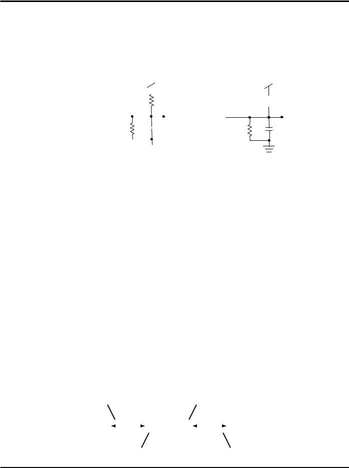
Figure 1. Output Test Load
(for tLZ, tHZ, tWZ, tOW)
3.3V
 590Ω
590Ω
DATAOUT
435Ω |
5pF |
2911 drw 05
Figure 2. Output Test Load (for tLZ, tHZ, tWZ, tOW)
* Including scope and jig.
AC ELECTRICAL CHARACTERISTICS OVER THE
OPERATING TEMPERATURE AND SUPPLY VOLTAGE RANGE(4)
|
|
|
IDT70V24X25 |
IDT70V24X35 |
IDT70V24X55 |
|
|
|||
|
|
|
|
|
|
|
|
|
|
|
|
Symbol |
Parameter |
Min. |
Max. |
Min. |
Max. |
Min. |
Max. |
|
Unit |
|
|
|
|
|
|
|
|
|
|
|
|
READ CYCLE |
|
|
|
|
|
|
|
|
|
|
tRC |
Read Cycle Time |
25 |
— |
35 |
— |
55 |
— |
|
ns |
|
|
|
|
|
|
|
|
|
|
|
|
tAA |
Address Access Time |
— |
25 |
— |
35 |
— |
55 |
|
ns |
|
|
|
|
|
|
|
|
|
|
|
|
tACE |
Chip Enable Access Time(3) |
— |
25 |
— |
35 |
— |
55 |
|
ns |
|
tABE |
Byte Enable Access Time(3) |
— |
25 |
— |
35 |
— |
55 |
|
ns |
|
tAOE |
Output Enable Access Time |
— |
15 |
— |
20 |
— |
30 |
|
ns |
|
|
|
|
|
|
|
|
|
|
|
|
tOH |
Output Hold from Address Change |
3 |
— |
3 |
— |
3 |
— |
|
ns |
|
tLZ |
Output Low-Z Time(1, 2) |
3 |
— |
3 |
— |
3 |
— |
|
ns |
|
tHZ |
Output High-Z Time(1, 2) |
— |
15 |
— |
20 |
— |
25 |
|
ns |
|
tPU |
Chip Enable to Power Up Time(2) |
0 |
— |
0 |
— |
0 |
— |
|
ns |
|
tPD |
Chip Disable to Power Down Time(2) |
— |
25 |
— |
35 |
— |
50 |
|
ns |
|
tSOP |
Semaphore Flag Update Pulse (OE or SEM) |
15 |
— |
15 |
— |
15 |
— |
|
ns |
|
|
|
|
|
|
|
|
|
|
|
|
tSAA |
Semaphore Address Access Time |
— |
35 |
— |
45 |
— |
65 |
|
ns |
|
|
|
|
|
|
|
|
|
|
|
|
NOTES: |
|
|
|
|
|
|
|
2911 tbl 11 |
|
1.Transition is measured ±200mV from Low or High-impedance voltage with Output Test Load (Figure 2).
2.This parameter is guaranteed by device characterization, but is not production tested.
3.To access RAM, CE = VIL, UB or LB = VIL, and SEM = VIH. To access semaphore, CE = VIH or UB and LB = VIH, and SEM = VIL.
4."X" in part numbers indicates power rating (S or L).
TIMING OF POWER-UP POWER-DOWN
CE |
|
|
|
|
|
|
|
|
|
|
|
|
|
|
|
|
|
|
|
|
|
|
|
|
|
|
|
|
|
|
|
|
|
|
|
|
|
|
|
|
|
|
|
|
|
|
|
|
|
|
|
|
|
|
|
|
|
|
|
|
|
|
|
|
|
|
|
|
|
|
|
|
|
|
|
|
|
|
|
|
|
|
|
|
|
|
|
|
|
|
|
|
|
|
|
|
|
|
ICC |
|
|
|
|
|
|
|
tPU |
|
|
|
|
|
|
|
|
|
|
tPD |
|
|
|
|
|
||||||||
|
|
|
|
|
|
|
|
|
|
|
|
|
|
|
|
|
|
|
|
|
|
|
||||||||||
|
|
|
|
|
|
|
|
|
|
|
|
|
||||||||||||||||||||
|
|
|
|
|
|
|
|
|
|
|
|
|
|
|
|
|
|
|
|
|
|
|
|
|
|
|||||||
|
|
|
|
|
|
|
50% |
|
|
|
|
|
|
|
|
|
50% |
|||||||||||||||
ISB |
|
|
|
|
|
|
|
|
|
|
|
|
|
|
|
|
|
|
|
|
|
|
|
|
|
|
|
|||||
|
|
|
|
|
|
|
|
|
|
|
|
|
|
|
|
|
|
|
|
|
|
|
|
|
|
|
||||||
|
|
|
|
|
|
|
|
|
|
|
|
|
|
|
|
|
|
|
|
|
|
|||||||||||
|
|
|
|
|
|
|
|
|
|
|
|
|
|
|
|
|
|
|
|
|
|
|
|
|
|
|
|
|
|
|
|
|
2911 drw 06
6.38 |
6 |
 Loading...