


IDT70T651S010BCI
Integrated Device Technology Inc IDT70T651S010BCI, IDT70T651S010BF, IDT70T651S010BFI, IDT70T651S012BC, IDT70T651S012BCI Datasheet
...
©2003 Integrated Device Technology, Inc.
1
NOVEMBER 2003
DSC-5632/3
CE
0R
R/
W
R
CE
1R
BE
0R
BE
1R
BE
2R
BE
3R
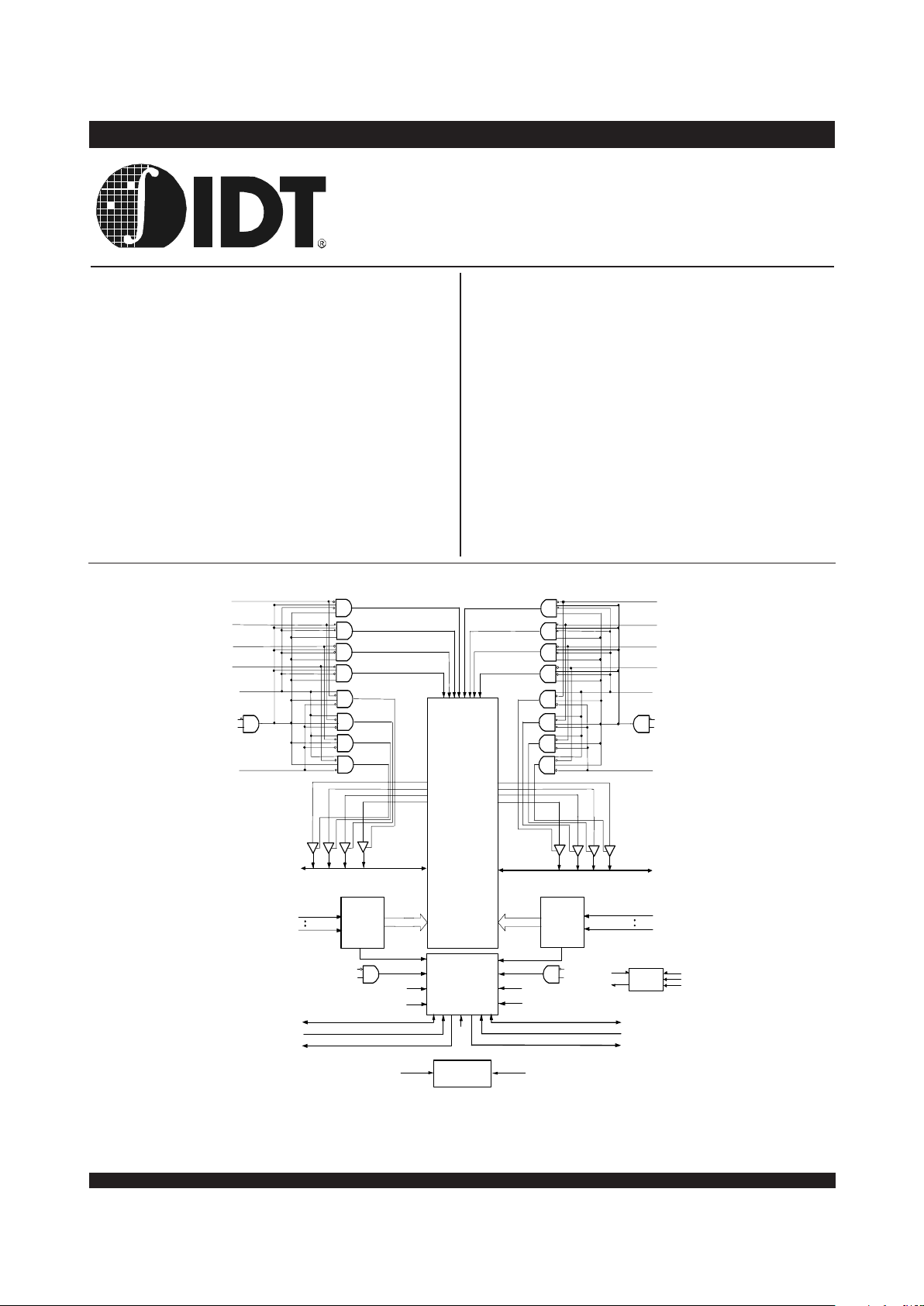
256/128K x 36
MEMORY
ARRAY
Address
Decoder
A
17R
(1)
A
0R
Address
Decoder
CE
0L
R/
W
L
CE
1L
BE
0L
BE
1L
BE
2L
BE
3L
Dout0-8_L
Dout9-17_L
Dout18-26_L
Dout27-35_L
Dout0-8_R
Dout9-17_R
Dout18-26_R
Dout27-35_R
B
E
0
L
B
E
1
L
B
E
2
L
B
E
3
L
B
E
3
R
B
E
2
R
B
E
1
R
B
E
0
R
I/O
0L-
I/O
35L
A
17L
(1)
A
0L
I/O
0R -
I/O
35R
Di n_L
ADDR_L
Di n_R
ADDR_R
OE
R
OE
L
ARBITRATION
INTERRUPT
SEMAPHORE
LOGIC
SEM
L
INT
L
(3)
BUSY
L
(2,3)
M/S
R/W
L
OE
L
R/W
R
OE
R
CE
0L
CE
1L
CE
0R
CE
1R
BUSY
R
(2,3)
SEM
R
INT
R
(3)
4869 drw 01
ZZ
CONTROL
LOGIC
ZZ
L
(4)
ZZ
R
(4)
JTAG
TC K
TRST
TMS
TDI
TD O
Functional Block Diagram
◆◆
◆◆
◆
Busy and Interrupt Flags
◆◆
◆◆
◆
On-chip port arbitration logic
◆◆
◆◆
◆
Full on-chip hardware support of semaphore signaling
between ports
◆◆
◆◆
◆
Fully asynchronous operation from either port
◆
Separate byte controls for multiplexed bus and bus
matching compatibility
◆◆
◆◆
◆
Sleep Mode Inputs on both ports
◆◆
◆◆
◆
Supports JTAG features compliant to IEEE 1149.1
◆◆
◆◆
◆
Single 2.5V (±100mV) power supply for core
◆◆
◆◆
◆
LVTTL-compatible, selectable 3.3V (±150mV)/2.5V (±100mV)
power supply for I/Os and control signals on each port
◆◆
◆◆
◆
Available in a 256-ball Ball Grid Array, 208-pin Plastic Quad
Flatpack and 208-ball fine pitch Ball Grid Array.
◆◆
◆◆
◆
Industrial temperature range (–40°C to +85°C) is available
for selected speeds
Features
◆◆
◆◆
◆
True Dual-Port memory cells which allow simultaneous
access of the same memory location
◆◆
◆◆
◆
High-speed access
– Commercial: 8/10/12/15ns (max.)
– Industrial: 10/12ns (max.)
◆◆
◆◆
◆
RapidWrite Mode simplifies high-speed consecutive write
cycles
◆◆
◆◆
◆
Dual chip enables allow for depth expansion without
external logic
◆◆
◆◆
◆
IDT70T651/9 easily expands data bus width to 72 bits or
more using the Master/Slave select when cascading more
than one device
◆◆
◆◆
◆
M/S = VIH for BUSY output flag on Master,
M/S = VIL for BUSY input on Slave
HIGH-SPEED 2.5V
256/128K x 36
ASYNCHRONOUS DUAL-PORT
STATIC RAM
WITH 3.3V 0R 2.5V INTERFACE
PRELIMINARY
IDT70T651/9S
NOTES:
1. Address A
17x is a NC for IDT70T659.
2. BUSY is an input as a Slave (M/S=V
IL) and an output when it is a Master (M/S=VIH).
3. BUSY and INT are non-tri-state totem-pole outputs (push-pull).
4. The sleep mode pin shuts off all dynamic inputs, except JTAG inputs, when asserted. OPTx, INTx, M/S and the sleep
mode pins themselves (ZZx) are not affected during sleep mode.

IDT70T651/9S Preliminary
High-Speed 2.5V 256/128K x 36 Asynchronous Dual-Port Static RAM Industrial and Commercial Temperature Ranges
2
Description
The IDT70T651/9 is a high-speed 256/128K x 36 Asynchronous
Dual-Port Static RAM. The IDT70T651/9 is designed to be used as a
stand-alone 9216/4608K-bit Dual-Port RAM or as a combination MASTER/SLAVE Dual-Port RAM for 72-bit-or-more word system. Using the
IDT MASTER/SLAVE Dual-Port RAM approach in 72-bit or wider
memory system applications results in full-speed, error-free operation
without the need for additional discrete logic.
This device provides two independent ports with separate control,
address, and I/O pins that permit independent, asynchronous access for
reads or writes to any location in memory. An automatic power down
feature controlled by the chip enables (either CE
0 or CE1) permit the
on-chip circuitry of each port to enter a very low standby power mode.
The IDT70T651/9 has a RapidWrite Mode which allows the designer
to perform back-to-back write operations without pulsing the R/W input
each cycle. This is especially significant at the 8 and 10ns cycle times of
the IDT70T651/9, easing design considerations at these high performance levels.
The 70T651/9 can support an operating voltage of either 3.3V or 2.5V
on one or both ports, controlled by the OPT pins. The power supply for
the core of the device (VDD) is at 2.5V.
3
IDT70T651/9S Preliminary
High-Speed 2.5V 256/128K x 36 Asynchronous Dual-Port Static RAM Industrial and Commercial Temperature Ranges
Pin Configuration
(1,2,3)
NOTES:
1. All V
DD pins must be connected to 2.5V power supply.
2. All V
DDQ pins must be connected to appropriate power supply: 3.3V if OPT pin for that port is set to VDD (2.5V), and 2.5V if OPT pin for that port is
set to V
SS (0V).
3. All V
SS pins must be connected to ground supply.
4. A
17X is a NC for IDT70T659.
5. Package body is approximately 17mm x 17mm x 1.4mm, with 1.0mm ball-pitch.
6. This package code is used to reference the package diagram.
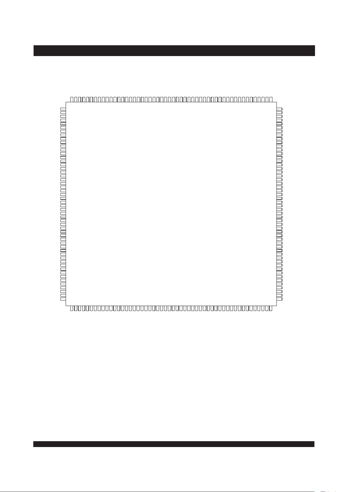
70T651/9BC
BC-256
(5,6)
256-Pin BGA
Top View
E16
I/O
14R
D16
I/O
16R
C16
I/O
16L
B16
NC
A16
NC
A15
NC
B15
I/O
17L
C15
I/O
17R
D15
I/O
15L
E15
I/O
14L
E14
I/O
13L
D14
I/O
15R
D13
V
DD
C12
A
6L
C14
OPT
L
B14
NC
A14
A
0L
A12
A
5L
B12
A
4L
C11
BUSY
L
D12
V
DDQR
D11
V
DDQR
C10
SEM
L
B11
NC
A11
INT
L
D8
V
DDQR
C8
BE
1L
A9
CE
1L
D9
V
DDQL
C9
BE
0L
B9
CE
0L
D10
V
DDQL
C7
A
7L
B8
BE
3L
A8
BE
2L
B13
A
1L
A13
A
2L
A10
OE
L
D7
V
DDQR
B7
A
9L
A7
A
8L
B6
A
12L
C6
A
10L
D6
V
DDQL
A5
A
14L
B5
A
15L
C5
A
13L
D5
V
DDQL
A4
A
17L
(4)
B4
NC
C4
A
16L
D4
V
DD
A3
NC
B3
TDO
C3
V
SS
D3
I/O
20L
D2
I/O
19R
C2
I/O
19L
B2
NC
A2
TDI
A1
NC
B1
I/O
18L
C1
I/O
18R
D1
I/O
20R
E1
I/O
21R
E2
I/O
21L
E3
I/O
22L
E4
V
DDQL
F1
I/O
23L
F2
I/O
22R
F3
I/O
23R
F4
V
DDQL
G1
I/O
24R
G2
I/O
24L
G3
I/O
25L
G4
V
DDQR
H1
I/O
26L
H2
I/O
25R
H3
I/O
26R
H4
V
DDQR
J1
I/O
27L
J2
I/O
28R
J3
I/O
27R
J4
V
DDQL
K1
I/O
29R
K2
I/O
29L
K3
I/O
28L
K4
V
DDQL
L1
I/O
30L
L2
I/O
31R
L3
I/O
30R
L4
V
DDQR
M1
I/O
32R
M2
I/O
32L
M3
I/O
31L
M4
V
DDQR
N1
I/O
33L
N2
I/O
34R
N3
I/O
33R
N4
V
DD
P1
I/O
35R
P2
I/O
34L
P3
TMSP4A
16R
R1
I/O
35L
R2
NCR3TRSTR4NC
T1
NC
T2
TCKT3NCT4A
17R
(4)
P5
A
13R
R5
A
15R
P12
A
6R
P8
BE
1R
P9
BE
0R
R8
BE
3R
T8
BE
2R
P10
SEM
R
T11
INT
R
P11
BUSY
R
R12
A
4R
T12
A
5R
P13
A
3R
P7
A
7R
R13
A
1R
T13
A
2R
R6
A
12R
T5
A
14R
T14
A
0R
R14
OPT
R
P14
I/O
0L
P15
I/O
0R
R15
NC
T15NCT16
NC
R16
NC
P16
I/O
1L
N16
I/O
2R
N15
I/O
1R
N14
I/O
2L
M16
I/O
4L
M15
I/O
3L
M14
I/O
3R
L16
I/O
5R
L15
I/O
4R
L14
I/O
5L
K16
I/O
7L
K15
I/O
6L
K14
I/O
6R
J16
I/O
8L
J15
I/O
7R
J14
I/O
8R
H16
I/O
10R
H15
IO
9L
H14
I/O
9R
G16
I/O
11R
G15
I/O
11L
G14
I/O
10L
F16
I/O
12L
F14
I/O
12R
F15
I/O
13R
R9
CE
0R
R11
M/S
T6
A
11R
T9
CE
1R
A6
A
11L
B10
R/W
L
C13
A
3L
P6
A
10R
R10
R/W
R
R7
A
9R
T10
OE
R
T7
A
8R
,
E5
V
DD
E6
V
DD
E7
V
SS
E8
V
SS
E9
V
SS
E10
V
SS
E11
V
DD
E12
V
DD
E13
V
DDQR
F5
V
DD
F6
NC
F8
V
SS
F9
V
SS
F10
V
SS
F12
V
DD
F13
V
DDQR
G5
V
SS
G6
V
SS
G7
V
SS
G8
V
SS
G9
V
SS
G10
V
SS
G11
V
SS
G12
V
SS
G13
V
DDQL
H5
V
SS
H6
V
SS
H7
V
SS
H8
V
SS
H9
V
SS
H10
V
SS
H11
V
SS
H12
V
SS
H13
V
DDQL
J5
ZZ
R
J6
V
SS
J7
V
SS
J8
V
SS
J9
V
SS
J10
V
SS
J11
V
SS
J12
ZZ
L
J13
V
DDQR
K5
V
SS
K6
V
SS
K7
V
SS
K8
V
SS
L5
V
DD
L6
NC
L7
V
SS
L8
V
SS
M5
V
DD
M6
V
DD
M7
V
SS
M8
V
SS
N5
V
DDQR
N6
V
DDQR
N7
V
DDQL
N8
V
DDQL
K9
V
SS
K10
V
SS
K11
V
SS
K12
V
SS
L9
V
SS
L10
V
SS
L11
V
SS
L12
V
DD
M9
V
SS
M10
V
SS
M11
V
DD
M12
V
DD
N9
V
DDQR
N10
V
DDQR
N11
V
DDQL
N12
V
DDQL
K13
V
DDQR
L13
V
DDQL
M13
V
DDQL
N13
V
DD
F7
V
SS
F11
V
SS
5632 drw 02f
,
03/18/03
IDT70T651/9S Preliminary
High-Speed 2.5V 256/128K x 36 Asynchronous Dual-Port Static RAM Industrial and Commercial Temperature Ranges
4
NOTES:
1. All V
DD pins must be connected to 2.5V power supply.
2. All V
DDQ pins must be connected to appropriate power supply: 3.3V if OPT pin for that port is set to VDD (2.5V) and 2.5V if OPT pin for that port is
set to V
SS (0V).
3. All V
SS pins must be connected to ground.
4. A
17X is a NC for IDT70T659.
5. Package body is approximately 28mm x 28mm x 3.5mm.
6. This package code is used to reference the package diagram.
7. 8ns Commercial and 10ns Industrial speed grades are not available in the DR-208 package.
8. This text does not indicate orientation of the actual part-marking.
1
2
3
4
5
6
7
8
9
10
11
12
13
14
15
16
17
18
19
20
21
22
23
24
25
26
27
28
29
30
31
32
33
34
35
36
37
38
39
40
41
42
43
44
45
46
47
48
49
50
51
52
5
3
5
4
5
5
5
6
5
7
5
8
5
9
6
0
6
1
6
2
6
3
6
4
6
5
6
6
6
7
6
8
6
9
7
0
7
1
7
2
7
3
7
4
7
5
7
6
7
7
7
8
7
9
8
0
8
1
8
2
8
3
8
4
8
5
8
6
8
7
8
8
8
9
9
0
9
1
9
2
9
3
9
4
9
5
9
6
9
7
9
8
9
9
1
0
0
1
0
1
1
0
2
1
0
3
1
0
4
156
155
154
153
152
151
150
149
148
147
146
145
144
143
142
141
140
139
138
137
136
135
134
133
132
131
130
129
128
127
126
125
124
123
122
121
120
119
118
117
116
115
114
113
112
111
110
109
108
107
106
105
2
0
8
2
0
7
2
0
6
2
0
5
2
0
4
2
0
3
2
0
2
2
0
1
2
0
0
1
9
9
1
9
8
1
9
7
1
9
6
1
9
5
1
9
4
1
9
3
1
9
2
1
9
1
1
9
0
1
8
9
1
8
8
1
8
7
1
8
6
1
8
5
1
8
4
1
8
3
1
8
2
1
8
1
1
8
0
1
7
9
1
7
8
1
7
7
1
7
6
1
7
5
1
7
4
1
7
3
1
7
2
1
7
1
1
7
0
1
6
9
1
6
8
1
6
7
1
6
6
1
6
5
1
6
4
1
6
3
1
6
2
1
6
1
1
6
0
1
5
9
1
5
8
1
5
7
70T651/9DR
DR-208
(5,6,7)
208-Pin
PQFP
Top View
(8)
I/O
19L
I/O
19R
I/O
20L
I/O
20R
V
DDQL
V
SS
I/O
21L
I/O
21R
I/O
22L
I/O
22R
V
DDQR
V
SS
I/O
23L
I/O
23R
I/O
24L
I/O
24R
V
DDQL
V
SS
I/O
25L
I/O
25R
I/O
26L
I/O
26R
V
DDQR
ZZ
R
V
DD
V
DD
V
SS
V
SS
V
DDQL
V
SS
I/O
27R
I/O
27L
I/O
28R
I/O
28L
V
DDQR
V
SS
I/O
29R
I/O
29L
I/O
30R
I/O
30L
V
DDQL
V
SS
I/O
31R
I/O
31L
I/O
32R
I/O
32L
V
DDQR
V
SS
I/O
33R
I/O
33L
I/O
34R
I/O
34L
V
S
S
V
D
D
Q
L
I
/
O
3
5
R
I
/
O
3
5
L
V
D
D
T
M
S
T
C
K
T
R
S
T
N
C
N
C
A
1
7
R
(
4
)
A
1
6
R
A
1
5
R
A
1
4
R
A
1
3
R
A
1
2
R
A
1
1
R
A
1
0
R
A
9
R
A
8
R
A
7
R
B
E
3
R
B
E
2
R
B
E
1
R
B
E
0
R
C
E
1
R
C
E
0
R
V
D
D
V
D
D
V
S
S
V
S
S
S
E
M
R
O
E
R
R
/
W
R
B
U
S
Y
R
I
N
T
R
M
/
S
A
6
R
A
5
R
A
4
R
A
3
R
A
2
R
A
1
R
A
0
R
V
D
D
V
S
S
V
S
S
O
P
T
R
I
/
O
0
L
I
/
O
0
R
V
D
D
Q
L
V
S
S
I/O
16L
I/O
16R
I/O
15L
I/O
15R
V
SS
V
DDQL
I/O
14L
I/O
14R
I/O
13L
I/O
13R
V
SS
V
DDQR
I/O
12L
I/O
12R
I/O
11L
I/O
11R
V
SS
V
DDQL
I/O
10L
I/O
10R
I/O
9L
I/O
9R
V
SS
V
DDQR
V
DD
V
DD
V
SS
V
SS
ZZ
L
V
DDQL
I/O
8R
I/O
8L
I/O
7R
I/O
7L
V
SS
V
DDQR
I/O
6R
I/O
6L
I/O
5R
I/O
5L
V
SS
V
DDQL
I/O
4R
I/O
4L
I/O
3R
I/O
3L
V
SS
V
DDQR
I/O
2R
I/O
2L
I/O
1R
I/O
1L
V
S
S
V
D
D
Q
R
I
/
O
1
8
R
I
/
O
1
8
L
V
S
S
V
D
D
T
D
I
T
D
O
N
C
N
C
A
1
7
L
(
4
)
A
1
6
L
A
1
5
L
A
1
4
L
A
1
3
L
A
1
2
L
A
1
1
L
A
1
0
L
A
9
L
A
8
L
A
7
L
B
E
3
L
B
E
2
L
B
E
1
L
B
E
0
L
C
E
1
L
C
E
0
L
V
D
D
V
D
D
V
S
S
V
S
S
S
E
M
L
O
E
L
R
/
W
L
B
U
S
Y
L
I
N
T
L
N
C
A
6
L
A
5
L
A
4
L
A
3
L
A
2
L
A
1
L
A
0
L
V
D
D
V
D
D
V
S
S
O
P
T
L
I
/
O
1
7
L
I
/
O
1
7
R
V
D
D
Q
R
V
S
S
5632 drw 02d
03/18/03
Pin Configurations
(1,2,3)
(con't.)

5
IDT70T651/9S Preliminary
High-Speed 2.5V 256/128K x 36 Asynchronous Dual-Port Static RAM Industrial and Commercial Temperature Ranges
Pin Configurations
(1,2,3)
(con't.)
NOTES:
1. All V
DD pins must be connected to 2.5V power supply.
2. All V
DDQ pins must be connected to appropriate power supply: 3.3V if OPT pin for that port is set to VDD (2.5V) and 2.5V if OPT pin for that port is
set to V
SS (0V).
3. All V
SS pins must be connected to ground.
4. A
17X is a NC for IDT70T659.
5. Package body is approximately 15mm x 15mm x 1.4mm with 0.8mm ball pitch.
6. This package code is used to reference the package diagram.
7. This text does not indicate orientation of the actual part-marking.
1716
15
1412 13
10
9876543
21
11
A
B
C
D
E
F
G
H
J
K
L
M
N
P
R
T
U
I/O
19L
I/O
18LVSS
A4
L
INT
L
SEM
L
BE
1L
A
8L
A
12L
A
16L
V
SS
I/O
17L
OPT
L
A
0L
I/O
20RVSS
I/O
18R
NC
A
1L
A5
L
BUSY
L
V
SS
CE
0L
CE
1L
BE
2L
A
9L
A
13L
A
17L
(4)
I/O16L
V
DDQR
V
SS
V
DDQL
I/O
19R
V
DDQ R
V
DD
A
2L
A6
L
R/
W
L
V
SS
BE
3L
A
10L
A
14L
NC I/O
15L
I/O
16R
V
DD
I/O
22LVSS
I/O
21L
I/O
20L
V
DD
A
3
L
NC
OE
L
I/O
23L
I/O
22RVDDQR
I/O
21R
V
DDQL
I/O
23R
I/O
24LVSS
I/O
26LVSS
I/O
25L
I/O
24R
V
DD
I/O
26R
V
DDQ R
I/O
25R
V
DDQ L
V
DD
VSSZZ
R
I/O
29R
I/O
28LVDDQR
V
DDQL
I/O
29L
I/O
30RVSS
I/O
14R
V
DDQL
I/O
14L
A
15LA11LA7L
BE
0L
I/O
12L
I/O
13R
V
SS
I/O
13L
V
SS
I/O
12R
I/O
11L
I/O9LV
DDQL
I/O
10L
I/O
11R
VDDI/O
9R
VSSI/O
10R
ZZ
L
V
DDQR
I/O
7R
V
DDQL
I/O8R
V
SS
I/O
8L
V
SS
I/O
7L
I/O
6R
A
0R
A
1R
A
2R
A
3R
A
4R
A
5R
A
6R
I/O
3R
I/O
31LVSS
I/O
31R
I/O
30L
A
16RA12RA8R
BE
1R
V
DD
SEM
R
INT
R
V
DDQR
I/O2LI/O
3L
I/O
4L
VSSI/O
33L
I/O
34R
NC
A
13RA9R
BE
2R
CE
0
R
CE
1R
V
DD
V
SS
BUS Y
R
V
SS
V
DD
V
SS
V
DDQL
I/O1RV
DDQ R
I/O
33R
I/O
34LVDDQL
NC
A
17R
(4)
A
14RA10R
BE
3R
V
SS
I/O
4R
I/O
6L
V
SS
I/O
5R
I/O
2R
V
SS
I/O
35L
V
DD
A
15R
A
11RA7R
BE
0R
OE
R
M/
S
R/
W
R
V
DDQL
I/O
5L
OPTRI/O0LI/O
1L
70T651/9BF
BF-208
(5,6)
208-Ball
fpBGA
Top View
(7)
5632 drw 02e
I/O
27L
I/O
28RVSS
I/O
27R
V
SS
I/O
32R
I/O
32LVDDQR
I/O
35R
A
B
C
D
E
F
G
H
J
K
L
M
N
P
R
T
U
V
SS
I/O
0R
I/O
17R
V
DDQR
V
SS
V
DD
V
SS
I/O
15R
V
DD
V
DD
TDO
TDI
TCK
TMS
TRST
V
SS
03/18/03
IDT70T651/9S Preliminary
High-Speed 2.5V 256/128K x 36 Asynchronous Dual-Port Static RAM Industrial and Commercial Temperature Ranges
6
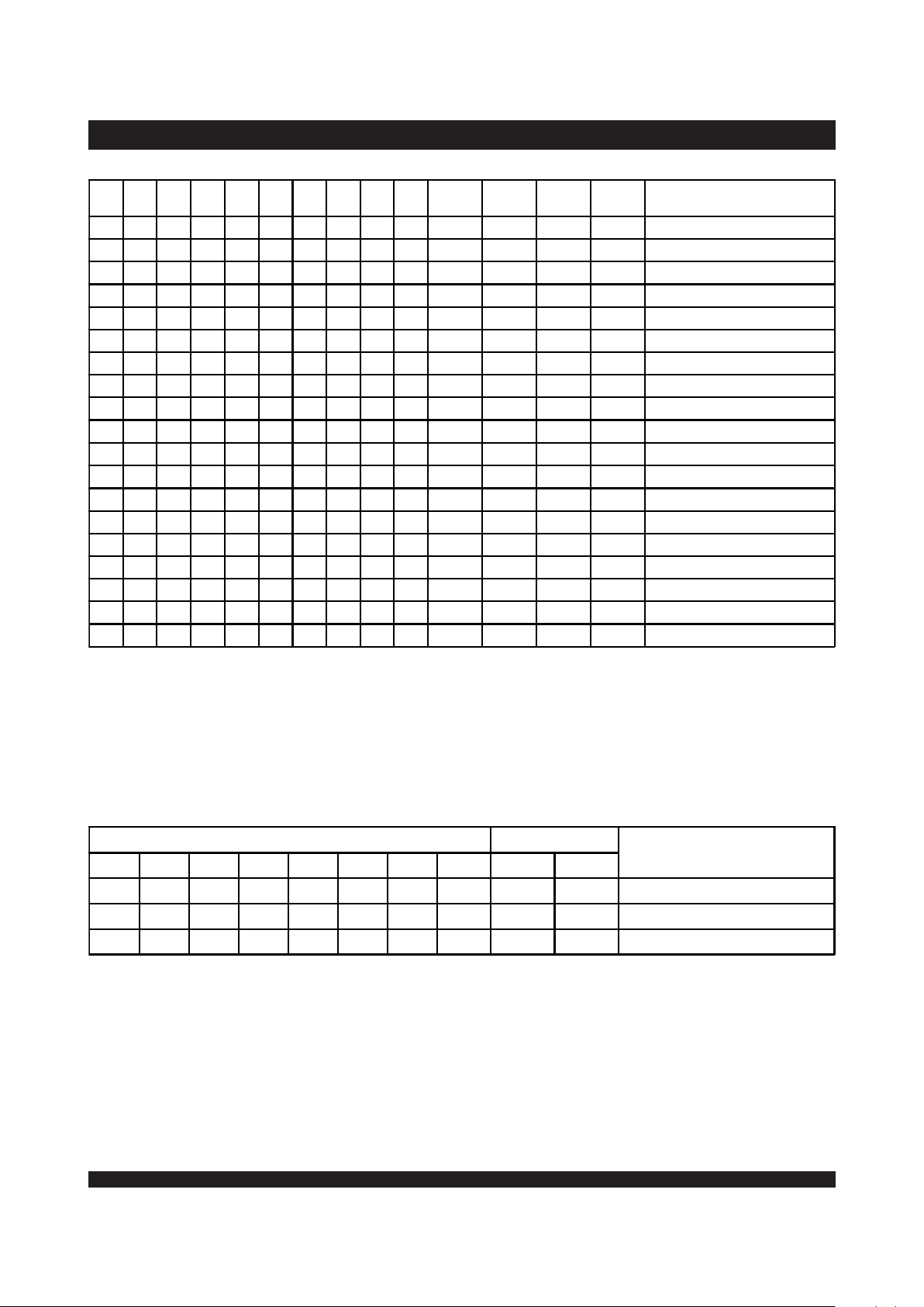
Pin Names
NOTES:
1. Address A
17x is a NC for IDT70T659.
2. V
DD, OPTX, and VDDQX must be set to appropriate operating levels prior to
applying inputs on I/O
X.
3. OPT
X selects the operating voltage levels for the I/Os and controls on that port.
If OPT
X is set to VDD (2.5V), then that port's I/Os and controls will operate at 3.3V
levels and V
DDQX must be supplied at 3.3V. If OPTX is set to VSS (0V), then that
port's I/Os and controls will operate at 2.5V levels and V
DDQX must be supplied
at 2.5V. The OPT pins are independent of one another—both ports can operate
at 3.3V levels, both can operate at 2.5V levels, or either can operate at 3.3V
with the other at 2.5V.
4. The sleep mode pin shuts off all dynamic inputs, except JTAG inputs, when
asserted. OPTx, INTx, M/S and the sleep mode pins themselves (ZZx) are
not affected during sleep mode. It is recommended that boundry scan not be
operated during sleep mode.
5. BUSY is an input as a Slave (M/S=V
IL) and an output when it is a Master
(M/S=V
IH).
Left Port Right Port Names
CE
0L
,
CE
1L
CE
0R
,
CE
1R
Chip Enables (Input)
R/W
L
R/W
R
Read /Write Enable (Inp ut)
OE
L
OE
R
Output Enable (Input)
A
0L
- A
17L
(1)
A0R - A
17R
(1)
Address (Input)
I/O
0L
- I/O
35L
I/O0R - I/O
35R
Data Inp ut/Outp ut
SEM
L
SEM
R
Semapho re Enable (Inp ut)
INT
L
INT
R
Interrup t Fl ag (Output)
BUSY
L
BUSY
R
Busy Flag (Output)
BE
0L
- BE
3L
BE0R - BE
3R
Byte Enab le s (9-bit by tes) (Input)
V
DDQL
V
DDQR
Power (I/O Bus) (3.3V or 2.5V)
(2)
(Input)
OPT
L
OPT
R
Optio n fo r sele c ting V
DDQX
(2,3 )
(Input)
ZZ
L
ZZ
R
Sleep Mode Pin
(4)
(Input)
M/S Master o r Slav e Select (Input)
(5)
V
DD
Power (2.5V)
(2)
(Input)
V
SS
Ground (0V) (Input)
TDI Test Data Inp ut
TDO Tes t Data Outp ut
TCK Test Lo gic Cloc k (10MHz) (Inp ut)
TMS Test Mode Select (Input)
TRST
Reset (Initialize TAP Contro ller) (Input)
5632 tbl 01
7
IDT70T651/9S Preliminary
High-Speed 2.5V 256/128K x 36 Asynchronous Dual-Port Static RAM Industrial and Commercial Temperature Ranges
NOTES:
1. "H" = V
IH, "L" = VIL, "X" = Don't Care.
2. It is possible to read or write any combination of bytes during a given access. A few representative samples have been illustrated here.
Truth Table I—Read/Write and Enable Control
(1,2)
OE SEM CE
0
CE
1
BE3BE2BE1BE
0
R/W ZZ
Byte 3
I/O
27-35
Byte 2
I/O
18-26
Byte 1
I/O
9-1 7
Byte 0
I/O
0-8
MODE
X H H X X X X X X L High-Z High-Z High-Z High-Z Deselected–Power Down
X H X L X X X X X L High-Z High-Z High-Z High-Z Deselected–Power Down
X H L H H H H H X L High-Z High-Z High-Z High-Z All Bytes Deselected
X H L H H H H L L L High-Z Hig h-Z High-Z D
IN
Write to Byte 0 Only
X H L H H H L H L L Hi gh-Z Hi gh- Z D
IN
High-Z Write to Byte 1 Only
XHL HHL HHL LHigh-Z D
IN
High-Z High-Z Write to Byte 2 Only
XHLHLHHHLL D
IN
High-Z High-Z High-Z Write to Byte 3 Only
X H L H H H L L L L Hig h-Z Hig h-Z D
IN
DINWrite to Lower 2 Byte s Only
XHLHLLHHLL D
IN
D
IN
High-Z High-Z Write to Upper 2 bytes Only
XHLHLLLLLL D
IN
D
IN
D
IN
DINWrite to All Bytes
L H L H H H H L H L High-Z Hig h-Z High-Z D
OUT
Read Byte 0 Only
LHLHHHLHHLHigh-ZHigh-Z D
OUT
High-Z Read Byte 1 Only
LHLHHLHHHLHigh-Z D
OUT
High-Z High-Z Read Byte 2 Only
LHLHLHHHHL D
OUT
High-Z High-Z High-Z Re ad By te 3 Only
LHLHHHLLHLHigh-ZHigh-Z D
OUT
D
OUT
Read Lower 2 Bytes Only
LHLHLLHHHL D
OUT
D
OUT
High-Z High-Z Read Upper 2 Bytes Only
LHLHLLLLHL D
OUT
D
OUT
D
OUT
D
OUT
Read All Bytes
H H L H L L L L X L High-Z High-Z High-Z High-Z Outputs Disabled
X X X X X X X X X H High-Z High-Z High-Z High-Z High-Z Sleep Mod e
5632 tb l 02
Truth Table II – Semaphore Read/Write Control
(1)
NOTES:
1. There are eight semaphore flags written to I/O
0 and read from all the I/Os (I/O0-I/O35). These eight semaphore flags are addressed by A0-A2.
2. CE = L occurs when CE
0 = VIL and CE1 = VIH. CE = H when CE0 = VIH and/or CE1 = VIL.
3. Each byte is controlled by the respective BEn. To read data BEn = V
IL.
Inputs
(1)
Outputs
Mode
CE
(2)
R/W
OE BE
3
BE
2
BE
1
BE
0
SEM
I/O
1-3 5
I/O
0
HHLLLLLLDATA
OUT
DATA
OUT
Read Data in Semaphore Flag
(3)
H
↑
XXXXL L X DATAINWrite I/O0 into Semaphore Flag
LXXXXXX L
______ ______
Not Allowed
5632 tbl 03
IDT70T651/9S Preliminary
High-Speed 2.5V 256/128K x 36 Asynchronous Dual-Port Static RAM Industrial and Commercial Temperature Ranges
8
Recommended Operating
Temperature and Supply Voltage
(1)
NOTE:
1. This is the parameter TA. This is the "instant on" case temperature.
Grade
Ambi ent
Temp erature GND V
DD
Commercial 0OC to +70OC0V2.5V + 100mV
Industrial -40
O
C to +85OC0V2.5V + 100mV
5632 tbl 04
NOTES:
1. These parameters are determined by device characterization, but are not
production tested.
2. 3dV references the interpolated capacitance when the input and output switch
from 0V to 3V or from 3V to 0V.
3. C
OUT also references CI/O.
Capacitance
(1)
(TA = +25°C, F = 1.0MHZ) PQFP ONLY
Symbol Parameter Conditions
(2)
Max. Unit
C
IN
Input Capacitance VIN = 3dV 8 pF
C
OUT
(3)
Outp ut Cap acitance V
OUT
= 3dV 10.5 pF
5632 tbl 08
NOTES:
1. Stresses greater than those listed under ABSOLUTE MAXIMUM RATINGS
may cause permanent damage to the device. This is a stress rating only and
functional operation of the device at these or any other conditions above those
indicated in the operational sections of this specification is not implied. Exposure
to absolute maximum rating conditions for extended periods may affect
reliability.
2. This is a steady-state DC parameter that applies after the power supply has
reached its nominal operating value. Power sequencing is not necessary;
however, the voltage on any Input or I/O pin cannot exceed V
DDQ during power
supply ramp up.
3. Ambient Temperature under DC Bias. No AC Conditions. Chip Deselected.
Recommended DC Operating
Conditions with V
DDQ at 2.5V
Symbol Parameter Min. Typ. Max. Unit
V
DD
Core Supp ly Voltag e 2.4 2.5 2.6 V
V
DDQ
I/O Supply Voltage
(3)
2.4 2.5 2.6 V
V
SS
Ground 0 0 0 V
V
IH
Inp ut Hi gh Vo lltage
(Address, Control &
Data I/ O Inputs)
(3)
1.7
____
V
DDQ
+ 100mV
(2)
V
V
IH
Inp ut Hi gh Vo ltag e
_
JTAG
1.7
____
V
DD
+ 100m V
(2)
V
V
IH
Input High Voltage -
ZZ, OP T, M /S
V
DD
- 0.2V
____
V
DD
+ 100m V
(2)
V
V
IL
Inp ut Lo w Voltag e -0.3
(1)
____
0.7 V
V
IL
Input Low Voltage -
ZZ, OP T, M /S
-0.3
(1)
____
0.2 V
5632 tb l 05
NOTES:
1. V
IL (min.) = -1.0V for pulse width less than tRC/2 or 5ns, whichever is less.
2. V
IH (max.) = V DDQ + 1.0V for pulse width less than tRC/2 or 5ns, whichever is
less.
3. To select operation at 2.5V levels on the I/Os and controls of a given port, the
OPT pin for that port must be set to V
SS(0V), and VDDQX for that port must be
supplied as indicated above.
Absolute Maximum Ratings
(1)
Symbol Rating Commercial
& Ind ustri al
Unit
V
TE R M
(VDD)
V
DD
Terminal Voltag e
with Re spec t to GND
-0.5 to 3.6 V
V
TE R M
(2 )
(V
DDQ
)
V
DDQ
Te rminal Voltage
with Re spec t to GND
-0.3 to V
DDQ
+ 0.3 V
V
TER M
(2)
(INPUTS and I/O' s)
Input and I/O Terminal
Voltage with Respect to GND
-0.3 to V
DDQ
+ 0.3 V
T
BIAS
(3)
Tempe rature
Under Bias
-55 to +125
o
C
T
STG
Storage
Tempe rature
-65 to +150
o
C
T
JN
Junc tio n Tempe rature +150
o
C
I
OUT
(Fo r V
DDQ =
3.3V ) DC Output Curre nt 50 mA
I
OUT
(Fo r V
DDQ =
2.5V ) DC Output Curre nt 40 mA
5632 tbl 07
NOTES:
1. V
IL (min.) = -1.0V for pulse width less than tRC/2 or 5ns, whichever is less.
2. V
IH (max.) = V DDQ + 1.0V for pulse width less than tRC/2 or 5ns, whichever is
less.
3. To select operation at 3.3V levels on the I/Os and controls of a given port, the
OPT pin for that port must be set to V
DD (2.5V), and VDDQX for that port must be
supplied as indicated above.
Recommended DC Operating
Conditions with V
DDQ at 3.3V
Symbol Parameter Min. Typ. Max. Unit
V
DD
Core Sup ply Voltag e 2.4 2. 5 2.6 V
V
DDQ
I/O Supply Voltage
(3)
3.15 3. 3 3. 45 V
V
SS
Ground 0 0 0 V
V
IH
Input Hig h Vo ltag e
(Add re ss , Co ntrol
&Data I/O Inp uts )
(3)
2.0
____
V
DDQ
+ 150mV
(2)
V
V
IH
Input Hig h Vo ltag e
_
JTAG
1.7
____
V
DD
+ 100m V
(2)
V
V
IH
Input High Voltage -
ZZ, O P T, M/S
V
DD
- 0.2V
____
V
DD
+ 100m V
(2)
V
V
IL
Input Lo w Voltag e -0.3
(1)
____
0.8 V
V
IL
Input Lo w Vol tag e -
ZZ, O P T, M/S
-0.3
(1)
____
0.2 V
5632 tbl 06
9
IDT70T651/9S Preliminary
High-Speed 2.5V 256/128K x 36 Asynchronous Dual-Port Static RAM Industrial and Commercial Temperature Ranges
DC Electrical Characteristics Over the Operating
Temperature and Supply Voltage Range
(VDD = 2.5V ± 100mV)
NOTES:
1. V
DDQ is selectable (3.3V/2.5V) via OPT pins. Refer to page 6 for details.
2. Applicable only for TMS, TDI and TRST inputs.
3. Outputs tested in tri-state mode.
DC Electrical Characteristics Over the Operating
Temperature and Supply Voltage Range
(3)
(VDD = 2.5V ± 100mV)
NOTES:
1. At f = f
MAX, address and control lines (except Output Enable) are cycling at the maximum frequency read cycle of 1/tRC, using "AC TEST CONDITIONS" at input
levels of GND to 3.3V.
2. f = 0 means no address or control lines change. Applies only to input at CMOS level standby.
3. Port "A" may be either left or right port. Port "B" is the opposite from port "A".
4. V
DD = 3.3V, TA = 25°C for Typ, and are not production tested. IDD DC(f=0) = 100mA (Typ).
5. CE
X = VIL means CE0X = VIL and CE1X = VIH
CEX = VIH means CE0X = VIH or CE1X = VIL
CEX < 0.2V means CE0X < 0.2V and CE1X > VDDQX - 0.2V
CE
X > VDDQX - 0.2V means CE0X > VDDQX - 0.2V or CE1X < 0.2V.
"X" represents "L" for left port or "R" for right port.
6. I
SB1, ISB2 and ISB4 will all reach full standby levels (ISB3) on the appropriate port(s) if ZZL and /or ZZR = VIH.
7. 8ns Commercial and 10ns Industrial speed grades are available in BF-208 and BC-256 packages only.
70T651/9S8
(7)
Com'l Only
70T651/9S10
Com'l
& Ind
(7)
70T651/9S12
Com'l
& Ind
70T651/9S15
Com'l Only
Symbol Parameter Test Condition Version Typ.
(4)
Max. Typ.
(4)
Max. Typ.
(4)
Max. Typ.
(4)
Max. Unit
I
DD
Dynamic Operating
Current (Both
Ports Active)
CE
L
and CER= VIL,
Outputs Disabled
f = f
MAX
(1)
COM'L S 350 475 300 405 300 355 225 305
mA
IND S
____ ____
300 445 300 395
____ ____
I
SB1
(6)
Standb y Current
(Both P orts - TTL
Le ve l Inputs)
CE
L
= CER = V
IH
f = f
MAX
(1)
COM'L S 115 140 90 120 75 105 60 85
mA
IND S
____ ____
90 145 75 130
____ ____
I
SB2
(6)
Standb y Current
(One Port - TTL
Le ve l Inputs)
CE
"A"
= VIL and CE
"B"
= V
IH
(5)
Active Po rt Outputs Disable d,
f = f
MAX
(1)
COM'L S 240 315 200 265 180 230 150 200
mA
IND S
____ ____
200 290 180 255
____ ____
I
SB3
Full Standby Current
(Both P orts - CMOS
Le ve l Inputs)
Both Ports CEL and
CE
R
> VDD - 0.2V, VIN > VDD - 0.2V
or V
IN
< 0.2V, f = 0
(2)
COM'LS210210210210
mA
IND S
____ ____
220220
____ ____
I
SB4
(6)
Full Standby Current
(One Port - CMOS
Le ve l Inputs)
CE
"A"
< 0.2V and CE
"B"
> VDD - 0.2 V
(5)
VIN > VDD - 0.2V or VIN < 0.2V, Ac tiv e
Po rt, Outp uts Dis ab le d , f = f
MAX
(1)
COM'L S 240 315 200 265 180 230 150 200
mA
IND S
____ ____
200 290 180 255
____ ____
IZZSleep Mode Current
(Both P orts - TTL
Le ve l Inputs)
ZZ
L = ZZR = VIH
f = f
MAX
(1)
COM'LS210210210210
mA
IND S
____ ____
220220
____ ____
5632 tbl 10
Symbol Parameter Test Conditions
70T651/9S
UnitMin. Max.
|I
LI
| Inp ut Leakag e Curre nt
(1)
V
DDQ
= Max., VIN = 0V to V
DDQ
___
10 µ A
|I
LI
| JTAG & ZZ Input Leakag e Curre nt
(1,2)
V
DD =
Max., VIN = 0V to V
DD
___
+30 µA
|I
LO
| Outp ut Leakage Curre nt
(1,3)
CE0 = VIH or CE1 = VIL, V
OUT
= 0V to V
DDQ
___
10 µ A
V
OL
(3.3V) Outp ut Low Voltage
(1)
IOL = +4mA, V
DDQ
= Min.
___
0.4 V
V
OH
(3.3V) Output Hig h Voltag e
(1)
IOH = -4mA, V
DDQ
= Min. 2.4
___
V
V
OL
(2.5V) Outp ut Low Voltage
(1)
IOL = +2mA, V
DDQ
= Min.
___
0.4 V
V
OH
(2.5V) Output Hig h Voltag e
(1)
IOH = -2mA, V
DDQ
= Min. 2.0
___
V
5632 tbl 09
 Loading...