


Integrated Device Technology Inc IDT7007L55JI, IDT7007L55PFI, IDT7007S15G, IDT7007L15G, IDT7007L15J Datasheet
...
|
|
HIGH-SPEED |
IDT7007S/L |
32K x 8 DUAL-PORT |
|
STATIC RAM |
|
Features
True Dual-Ported memory cells which allow simultaneous reads of the same memory location
High-speed access
–Military: 25/35/55ns (max.)
–Industrial: 55ns (max.)
–Commercial: 15/20/25/35/55ns (max.)
Low-power operation
–IDT7007S
Active: 850mW (typ.) Standby: 5mW (typ.)
–IDT7007L
Active: 850mW (typ.) Standby: 1mW (typ.)
IDT7007 easily expands data bus width to 16 bits or more
using the Master/Slave select when cascading more than one device
M/S = H for BUSY output flag on Master, M/S = L for BUSY input on Slave
Interrupt Flag
On-chip port arbitration logic
Full on-chip hardware support of semaphore signaling between ports
Fully asynchronous operation from either port
TTL-compatible, single 5V (±10%) power supply
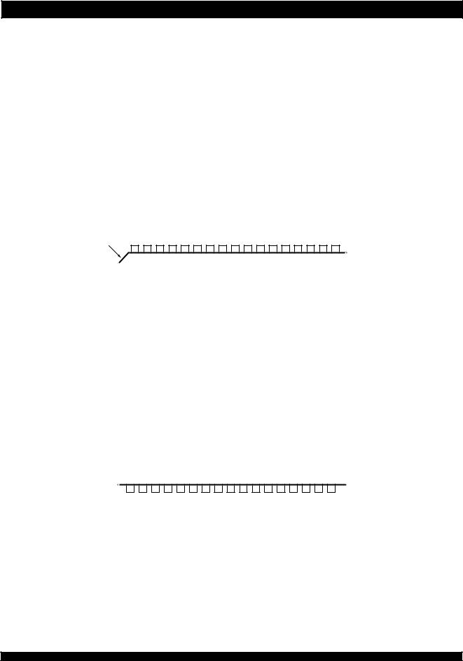
Available in 68-pin PGA and PLCC and a 80-pin TQFP
Industrial temperature range (–40°C to +85°C) is available for selected speeds
Functional Block Diagram
OEL |
CEL |
R/WL |
OER |
CER |
R/WR |
|
I/O0L- I/O7L |
I/O |
|
I/O |
I/O0R-I/O7R |
|
|
|
|
|
|
||
|
|
Control |
|
Control |
|
|
|
(1,2) |
|
|
|
|
(1,2) |
|
BUSYL |
|
|
|
BUSYR |
|
|
A14L |
Address |
MEMORY |
Address |
A14R |
|
|
|
|
|
|||
|
A0L |
Decoder |
ARRAY |
Decoder |
A0R |
|
|
|
15 |
|
15 |
|
|
|
|
|
|
|
|
|
|
|
CEL |
ARBITRATION |
|
|
|
|
|
INTERRUPT |
CER |
|
|
|
|
|
OEL |
SEMAPHORE |
OER |
|
|
|
|
R/WL |
LOGIC |
R/WR |
|
|
|
SEML |
|
M/S |
|
SEMR |
|
|
(2) |
|
|
|
INTR |
(2) |
|
INTL |
|
|
|
|
|
|
|
|
|
|
2940 drw 01 |
|
NOTES: |
|
|
|
|
|
|
1. (MASTER): BUSY is output; (SLAVE): BUSY is input. |
|
|
|
|
||
2. |
BUSY and INT outputs are non-tri-stated push-pull. |
|
|
|
|
|
JUNE 1999
1
DSC 2940/8
IDT7007S/L |
|
High-Speed 32K x 8 Dual-Port Static RAM |
Military, Industrial and Commercial Temperature Ranges |
Description
The IDT7007 is a high-speed 32K x 8 Dual-Port Static RAM. The IDT7007isdesignedtobeusedasastand-alone256K-bitDual-PortRAM or as a combination MASTER/SLAVE Dual-Port RAM for 16-bit-or-more wordsystems.UsingtheIDTMASTER/SLAVEDual-PortRAMapproach in 16-bit or wider memory system applications results in full-speed, errorfree operation without the need for additional discrete logic.
This device provides two independent ports with separate control, address, and I/O pins that permit independent, asynchronous access for reads or writes to any location in memory. An automatic power down
feature controlled by CE permits the on-chip circuitry of each port to enter a very LOW standby power mode.
Fabricated using IDT’s CMOS high-performance technology, these devices typically operate on only 850mW of power.
The IDT7007 is packaged in a 68-pin pin PGA, a 68-pin PLCC, and an 80-pin thin quad flatpack, TQFP. Military grade product is manufactured in compliance with the latest revision of MIL-PRF-38535 QML,ClassB,makingitideallysuitedtomilitarytemperatureapplications demanding the highest level of performance and reliability.
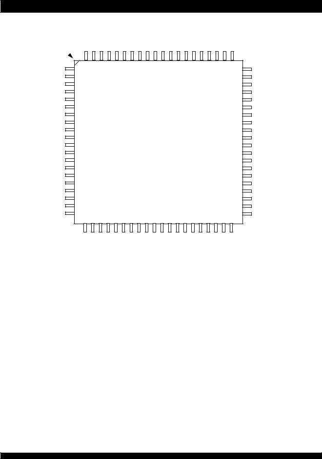
Pin Configurations(1,2,3)
INDEX |
I/O1L |
I/O0L |
N/C OEL |
WR/L |
SEML |
||||
I/O2L |
|
|
9 |
|
8 |
7 |
6 |
5 |
4 |
|
|
10 |
|
|
|
|
|
|
|
|
|
|
|
|
|
|
|
||
I/O3L |
|
|
11 |
|
|
|
|
|
|
|
|
|
|
|
|
|
|
||
I/O4L |
|
|
12 |
|
|
|
|
|
|
|
|
|
|
|
|
|
|||
|
|
|
|
|
|
|
|
||
I/O5L |
|
|
13 |
|
|
|
|
|
|
|
|
|
|
|
|
|
|
||
GND |
|
|
14 |
|
|
|
|
|
|
|
|
|
|
|
|
|
|||
|
|
|
|
|
|
|
|
||
I/O6L |
|
|
15 |
|
|
|
|
|
|
|
|
|
|
|
|
|
|||
|
|
|
|
|
|
|
|
||
I/O7L |
|
|
16 |
|
|
|
|
|
|
|
|
|
|
|
|
|
|||
|
|
|
|
|
|
|
|
||
VCC |
|
|
17 |
|
|
|
|
|
|
|
|
|
|
|
|
|
|||
|
|
|
|
|
|
|
|
||
GND |
|
|
18 |
|
|
|
|
|
|
|
|
|
|
|
|
|
|
||
I/O0R |
|
|
19 |
|
|
|
|
|
|
|
|
|
|
|
|
|
|||
|
|
|
|
|
|
|
|
||
I/O1R |
|
|
20 |
|
|
|
|
|
|
|
|
|
|
|
|
|
|||
|
|
|
|
|
|
|
|
||
I/O2R |
|
|
21 |
|
|
|
|
|
|
|
|
|
|
|
|
|
|||
|
|
|
|
|
|
|
|
||
VCC |
|
|
22 |
|
|
|
|
|
|
|
|
|
|
|
|
|
|||
|
|
|
|
|
|
|
|
||
I/O3R |
|
|
23 |
|
|
|
|
|
|
|
|
|
|
|
|
|
|||
|
|
|
|
|
|
|
|
||
I/O4R |
|
|
24 |
|
|
|
|
|
|
|
|
|
|
|
|
|
|||
|
|
|
|
|
|
|
|
||
I/O5R |
|
|
25 |
|
|
|
|
|
|
|
|
|
|
|
|
|
|||
|
|
|
|
|
|
|
|
||
I/O6R |
|
|
26 |
|
|
|
|
|
|
|
|
|
|
|
|
|
|||
|
|
|
|
|
|
|
|
||
|
|
|
27 |
28 29 |
30 31 |
32 |
|||
CEL |
A14L |
A13L |
VCC |
A12L |
A11L |
A10L |
A9L |
A8L |
A7L |
A6L |
|
|
||||||
3 |
2 |
1 |
68 |
67 66 |
65 64 |
63 62 61 |
|
A5L |
||||||||||
|
||||||||||||||||||
|
|
|
|
|
|
|
|
|
|
|
|
|
|
|
60 |
|
||
|
|
|
|
|
|
|
|
|
|
|
|
|
|
|
|
|||
|
|
|
|
|
|
|
|
|
|
|
|
|
|
|
59 |
|
A4L |
|
|
|
|
|
|
|
|
|
|
|
|
|
|
|
|
|
|||
|
|
|
|
|
|
|
|
|
|
|
|
|
|
|
58 |
|
A3L |
|
|
|
|
|
|
|
|
|
|
|
|
|
|
|
|
|
|||
|
|
|
|
|
|
|
|
|
|
|
|
|
|
|
|
|||
|
|
|
|
|
|
|
|
|
|
|
|
|
|
|
57 |
|
A2L |
|
|
|
|
|
|
|
|
|
|
|
|
|
|
|
|
|
|||
|
|
|
|
|
|
|
|
|
|
|
|
|
|
|
|
|||
|
|
|
|
|
|
|
|
|
|
|
|
|
|
|
56 |
|
A1L |
|
|
|
|
|
|
|
|
|
|
|
|
|
|
|
|
|
|||
|
|
|
|
|
|
|
|
|
|
|
|
|
|
|
|
|||
IDT7007J |
|
|
|
|
|
|
|
|
|
|
|
55 |
|
A0L |
||||
|
|
|
|
|
|
|
|
|
|
|
|
|||||||
|
|
|
|
|
|
|
|
|
|
|
|
|||||||
|
|
|
|
|
|
|
|
|
|
|
54 |
|
INTL |
|||||
|
|
|
|
|
|
|
|
|
|
|
|
|||||||
|
J68-1(4) |
|
|
|
|
|
|
|
|
|
|
|
|
|||||
|
|
|
|
|
|
|
|
|
|
|
|
|
||||||
|
|
|
|
|
|
|
|
|
|
|
|
53 |
|
BUSYL |
||||
|
|
|
|
|
|
|
|
|
|
|
|
|
||||||
|
|
|
|
|
|
|
|
|
|
|
|
|
|
|
|
|||
68-Pin PLCC |
|
|
|
|
|
|
|
|
|
|
52 |
|
GND |
|||||
|
|
|
|
|
|
|
|
|
|
|
||||||||
|
|
|
|
|
|
|
|
|
|
|
||||||||
Top View(5) |
|
|
|
|
|
|
|
|
|
|
|
51 |
|
M/S |
||||
|
|
|
|
|
|
|
|
|
|
|
|
|
|
|||||
|
|
|
|
|
|
|
|
|
|
|
50 |
|
BUSYR |
|||||
|
|
|
|
|
|
|
|
|
|
|
|
|
|
|
|
|||
|
|
|
|
|
|
|
|
|
|
|
|
|
|
|
49 |
|
INTR |
|
|
|
|
|
|
|
|
|
|
|
|
|
|
|
|
|
|||
|
|
|
|
|
|
|
|
|
|
|
|
|
|
|
|
|||
|
|
|
|
|
|
|
|
|
|
|
|
|
|
|
48 |
|
A0R |
|
|
|
|
|
|
|
|
|
|
|
|
|
|
|
|
|
|||
|
|
|
|
|
|
|
|
|
|
|
|
|
|
|
|
|||
|
|
|
|
|
|
|
|
|
|
|
|
|
|
|
47 |
|
A1R |
|
|
|
|
|
|
|
|
|
|
|
|
|
|
|
|
|
|||
|
|
|
|
|
|
|
|
|
|
|
|
|
|
|
|
|||
|
|
|
|
|
|
|
|
|
|
|
|
|
|
|
46 |
|
A2R |
|
|
|
|
|
|
|
|
|
|
|
|
|
|
|
|
|
|||
|
|
|
|
|
|
|
|
|
|
|
|
|
|
|
|
|||
|
|
|
|
|
|
|
|
|
|
|
|
|
|
|
45 |
|
A3R |
|
|
|
|
|
|
|
|
|
|
|
|
|
|
|
|
|
|||
|
|
|
|
|
|
|
|
|
|
|
|
|
|
|
|
|||
33 |
34 35 |
36 37 |
38 39 |
|
|
|
|
|
|
|
|
44 |
|
A4R |
||||
|
|
|
|
|
|
|
|
|
||||||||||
|
|
|
|
|
|
|
|
|
||||||||||
40 41 |
42 43 |
|
|
|||||||||||||||
|
|
|
|
|
|
|
|
|
|
|
|
|
|
|
|
|
|
|
|
|
|
|
|
|
|
|
|
|
|
|
|
|
|
|
|
|
|
I/O7R |
N/C OER |
WR/R |
SEMR |
CER |
NOTES:
1. All Vcc pins must be connected to power supply. 2. All GND pins must be connected to ground supply.
3. Package body is approximately .95 in x .95 in x .17 in.
4. This package code is used to reference the package diagram. 5. This text does not indicate orientation of the actual part marking.
A14R |
A13R |
GND A12R |
A11R |
A10R |
A9R |
A8R |
A7R |
A6R |
A5R |
2940 drw 02
2
IDT7007S/L |
|
High-Speed 32K x 8 Dual-Port Static RAM |
Military, Industrial and Commercial Temperature Ranges |
Pin Configurations(1,2,3) (con't.)
INDEX 

I/O1L |
I/O0L |
N/C OEL |
WR/L |
SEML |
CEL |
N/C A14L |
A13L |
VCC |
A12L |
A11L |
A10L |
A9L |
A8L |
A7L |
A6L |
N/C N/C |
N/C |
1 |
80 |
79 |
78 |
77 |
76 |
75 |
74 |
73 |
72 |
71 |
70 |
69 |
68 |
67 |
66 |
65 |
64 |
63 |
62 |
61 |
N/C |
|
|
|
|
|
|
|
|
|
|
|
|
|
|
|
|
|
|
|
60 |
|||
I/O2L |
2 |
|
|
|
|
|
|
|
|
|
|
|
|
|
|
|
|
|
|
|
59 |
A5L |
I/O3L |
3 |
|
|
|
|
|
|
|
|
|
|
|
|
|
|
|
|
|
|
|
58 |
A4L |
I/O4L |
4 |
|
|
|
|
|
|
|
|
|
|
|
|
|
|
|
|
|
|
|
57 |
A3L |
I/O5L |
5 |
|
|
|
|
|
|
|
|
|
|
|
|
|
|
|
|
|
|
|
56 |
A2L |
GND |
6 |
|
|
|
|
|
|
|
|
|
|
|
|
|
|
|
|
|
|
|
55 |
A1L |
I/O6L |
7 |
|
|
|
|
|
|
|
|
7007PF |
|
|
|
|
|
|
|
54 |
A0L |
|||
I/O7L |
8 |
|
|
|
|
|
|
|
|
|
|
|
|
|
|
|
53 |
INTL |
||||
|
|
|
|
|
|
|
|
PN80-1(4) |
|
|
|
|
|
|
|
|||||||
VCC |
9 |
|
|
|
|
|
|
|
|
|
|
|
|
|
|
|
52 |
BUSYL |
||||
N/C |
10 |
|
|
|
|
|
|
|
80-Pin TQFP |
|
|
|
|
|
|
51 |
GND |
|||||
GND |
11 |
|
|
|
|
|
|
|
|
|
|
|
|
|
50 |
M/S |
||||||
I/O0R |
12 |
|
|
|
|
|
|
|
Top View(5) |
|
|
|
|
|
|
49 |
BUSYR |
|||||
I/O1R |
13 |
|
|
|
|
|
|
|
|
|
|
|
|
|
|
|
|
|
|
|
48 |
INTR |
I/O2R |
14 |
|
|
|
|
|
|
|
|
|
|
|
|
|
|
|
|
|
|
|
47 |
A0R |
VCC |
15 |
|
|
|
|
|
|
|
|
|
|
|
|
|
|
|
|
|
|
|
46 |
A1R |
I/O3R |
16 |
|
|
|
|
|
|
|
|
|
|
|
|
|
|
|
|
|
|
|
45 |
A2R |
I/O4R |
17 |
|
|
|
|
|
|
|
|
|
|
|
|
|
|
|
|
|
|
|
44 |
3R |
|
|
|
|
|
|
|
|
|
|
|
|
|
|
|
|
|
|
|
|
|
A |
|
I/O5R |
18 |
|
|
|
|
|
|
|
|
|
|
|
|
|
|
|
|
|
|
|
43 |
A4R |
I/O6R |
19 |
|
|
|
|
|
|
|
|
|
|
|
|
|
|
|
|
|
|
|
42 |
N/C |
N/C |
20 |
|
22 |
23 |
24 |
25 |
26 |
27 |
28 |
29 |
30 |
31 |
32 |
33 |
34 |
35 |
36 |
37 |
38 |
39 |
41 |
N/C |
|
21 |
40 |
|
|||||||||||||||||||
|
I/O7R |
N/C OER |
WR/R |
SEMR |
CER |
N/C A14R |
A13R |
GND A12R |
A11R |
A10R |
A9R |
A8R |
A7R |
A6R |
A5R |
N/C N/C |
2940 drw 03 |
|||||
|
|
|||||||||||||||||||||
NOTES:
1. All Vcc pins must be connected to power supply. 2. All GND pins must be connected to ground supply.
3. Package body is approximately 14mm x 14mm x 1.4mm.
4. This package code is used to reference the package diagram. 5. This text does not indicate orientation of the actual part marking.
3

IDT7007S/L |
|
|
|
|
|
|
|
|
|
|
|
|
|
High-Speed 32K x 8 Dual-Port Static RAM |
|
|
|
|
Military, Industrial and Commercial Temperature Ranges |
||||||||
Pin Configurations(1,2,3) (con't.) |
|
|
|
|
|
|
|
|
|||||
|
|
|
|
|
|
|
|
|
|
|
|
|
|
11 |
|
51 |
50 |
48 |
|
46 |
44 |
42 |
40 |
38 |
36 |
|
|
|
A5L |
A4L |
A2L |
|
A0L |
BUSYL |
M/S |
INTR |
A1R |
A3R |
|
|
|
|
|
|
|
|
|
|
|
|
|
|
|
|
|
|
|
|
|
|
|
|
|
|
|
|
|
|
|
10 |
53 |
52 |
49 |
47 |
|
45 |
43 |
41 |
39 |
37 |
35 |
34 |
|
A7L |
A6L |
A3L |
A1L |
|
INTL |
GND |
BUSYR |
A0R |
A2R |
A4R |
A5R |
|
|
|
|
|
|||||||||||
|
|
|
|
|
|
|
|
|
|
|
|
|
|
09 |
55 |
54 |
|
|
|
|
|
|
|
|
32 |
33 |
|
A9L |
A8L |
|
|
|
|
|
|
|
|
A7R |
A6R |
|
|
|
|
|
|
|
|
|
|
|
|
|
|
|
|
08 |
57 |
56 |
|
|
|
|
|
|
|
|
30 |
31 |
|
A11L |
A10L |
|
|
|
|
|
|
|
|
A9R |
A8R |
|
|
|
|
|
|
|
|
|
|
|
|
|
|
|
|
07 |
59 |
58 |
|
|
|
IDT7007G |
|
|
28 |
29 |
|
||
VCC |
A12L |
|
|
|
|
|
A11R |
A10R |
|
||||
|
|
|
|
|
|
|
G68-1(4) |
|
|
|
|
|
|
06 |
61 |
60 |
|
|
|
|
|
|
26 |
27 |
|
||
|
|
|
|
|
|
|
|
|
|||||
A14L |
A13L |
|
|
|
68-Pin PGA |
|
|
GND |
A12R |
|
|||
|
|
|
|
|
|
|
|
|
|
|
|||
|
63 |
62 |
|
|
|
|
|
24 |
25 |
|
|||
05 |
|
|
|
Top View(5) |
|
|
|
||||||
SEML |
CEL |
|
|
|
|
|
A14R |
A13R |
|
||||
|
|
|
|
|
|
|
|
|
|
||||
|
|
|
|
|
|
|
|
|
|
|
|
|
|
04 |
65 |
64 |
|
|
|
|
|
|
|
|
22 |
23 |
|
OEL |
R/WL |
|
|
|
|
|
|
|
|
SEMR |
CER |
|
|
|
|
|
|
|
|
|
|
|
|
|
|
|
|
03 |
67 |
66 |
|
|
|
|
|
|
|
|
20 |
21 |
|
I/O0L |
N/C |
|
|
|
|
|
|
|
|
OER |
R/WR |
|
|
|
|
|
|
|
|
|
|
|
|
|
|
|
|
02 |
68 |
1 |
3 |
5 |
|
7 |
9 |
11 |
13 |
15 |
18 |
19 |
|
I/O1L |
I/O2L |
I/O4L |
GND |
|
I/O7L |
GND |
I/O1R |
VCC |
I/O4R |
I/O7R |
N/C |
|
|
|
|
|
|||||||||||
|
|
|
|
|
|
|
|
|
|
|
|
|
|
01 |
|
2 |
4 |
6 |
|
8 |
10 |
12 |
14 |
16 |
17 |
|
|
|
I/O3L |
I/O5L |
I/O6L |
|
VCC |
I/O0R |
I/O2R |
I/O3R |
I/O5R |
I/O6R |
|
|
|
|
|
|
|
|
|
|
|
|
|
|
|
|
|
|
A |
B |
C |
D |
E |
F |
G |
H |
J |
K |
L |
||
INDEX |
|
|
|
|
|
|
|
|
|
|
|
|
|
NOTES:
1. All Vcc pins must be connected to power supply 2. All GND pins must be connected to power supply
3. Package body is approximately 1.8 in x 1.8 in x .16 in.
4. This package code is used to reference the package diagram. 5. This text does not indicate orientation of the actual part marking.
|
|
|
2940 drw 04 |
Pin Names |
|
||
|
|
|
|
Left Port |
|
Right Port |
Names |
|
|
|
|
CEL |
|
CER |
Chip Enables |
|
|
|
|
R/WL |
|
R/WR |
Read/Write Enable |
|
|
|
|
OEL |
|
OER |
Output Enable |
|
|
|
|
A0L - A14L |
|
A0R - A14R |
Address |
|
|
|
|
I/O0L - I/O7L |
|
I/O0R - I/O7R |
Data Input/Output |
|
|
|
|
SEML |
|
SEMR |
Semaphore Enable |
|
|
|
|
INTL |
|
INTR |
Interrupt Flag |
|
|
|
|
BUSYL |
|
BUSYR |
Busy Flag |
|
|
|
|
|
M/S |
Master or Slave Select |
|
|
|
|
|
|
VCC |
Power |
|
|
|
|
|
|
GND |
Ground |
|
|
|
|
|
2940 tbl 01
4

IDT7007S/L |
|
High-Speed 32K x 8 Dual-Port Static RAM |
Military, Industrial and Commercial Temperature Ranges |
Truth Table I: Non-Contention Read/Write Control
|
Inputs(1) |
|
|
Outputs |
|
|
|
|
|
|
|
|
|
CE |
R/W |
|
OE |
SEM |
I/O0-7 |
Mode |
|
|
|
|
|
|
|
H |
X |
|
X |
H |
High-Z |
Deselected: Power-Down |
|
|
|
|
|
|
|
L |
L |
|
X |
H |
DATAIN |
Write to Memory |
|
|
|
|
|
|
|
L |
H |
|
L |
H |
DATAOUT |
Read Memory |
|
|
|
|
|
|
|
X |
X |
|
H |
X |
High-Z |
Outputs Disabled |
|
|
|
|
|
|
|
NOTE: |
2940 tbl 02 |
|
|
1. A0L — A14L ≠ A0R — A14R |
|
Truth Table II: Semaphore Read/Write Control(1)
|
|
Inputs |
|
|
Outputs |
|
|
|
|
|
|
|
|
|
|
CE |
R/W |
|
OE |
SEM |
|
I/O0-7 |
Mode |
|
|
|
|
|
|
|
|
H |
H |
|
L |
L |
|
DATAOUT |
Read Semap hore Flag Data Out (I/O0-I/O7) |
|
|
|
|
|
|
|
|
H |
↑ |
|
X |
L |
|
DATAIN |
Write I/O0 into Semaphore Flag |
|
|
|
|
|
|
|
|
L |
X |
|
X |
L |
|
______ |
Not Allowed |
|
|
|
|
|
|
|
|
|
|
|
|
|
|
|
|
NOTE: |
|
|
|
|
|
|
2940 tbl 03 |
|
|
|
|
|
|
|
|
1. There are eight semaphore flags written to via I/O0 |
and read from all I/O's. These eight semaphores are addressed by A0 - A2. |
||||||
Absolute Maximum Ratings(1)
Symbol |
Rating |
Commercial |
Military |
Unit |
|
|
& Industrial |
|
|
|
|
|
|
|
VTERM(2) |
Terminal Voltage |
-0.5 to +7.0 |
-0.5 to +7.0 |
V |
|
with Respect |
|
|
|
|
to GND |
|
|
|
|
|
|
|
|
TBIAS |
Temperature |
-55 to +125 |
-55 to +135 |
oC |
|
Under Bias |
|
|
|
|
|
|
|
|
TSTG |
Storage |
-55 to +120 |
-65 to +150 |
oC |
|
Temperature |
|
|
|
|
|
|
|
|
IOUT |
DC Output |
50 |
50 |
mA |
|
Current |
|
|
|
|
|
|
|
|
NOTES:
1. Stresses greater than those listed under ABSOLUTE MAXIMUM RATINGS may cause permanent damage to the device. This is a stress rating only and functional operation of the device at these or any other conditions above those indicated in the operational sec-tions of this specification is not implied. Exposure to absolute maxi-mum rating conditions for extended periods may affect reliability.
2. VTERM must not exceed Vcc + 10% for more than 25% of the cycle time or 10ns maximum, and is limited to < 20mA for the period of VTERM > Vcc + 10%.
Capacitance (TA = +25°C, f = 1.0mhz)
Symbol |
Parameter(1) |
Conditions(2) |
Max. |
Unit |
CIN |
Input Capacitance |
VIN = 3dV |
9 |
pF |
|
|
|
|
|
COUT |
Output Capacitance |
VOUT = 3dV |
10 |
pF |
|
|
|
|
|
NOTES:
1. This parameter is determined by device characterization but is not production tested. TQFP package only.
2. 3dV represents the interpolated capacitance when the input and output signals switch from 0V to 3V or from 3V to 0V.
Maximum Operating Temperature
and Supply Voltage(1,2)
|
Ambient |
|
|
|
Grade |
Temperature |
GND |
Vcc |
|
|
|
|
|
|
Military |
-55OC to+125OC |
0V |
5.0V |
+ 10% |
Commercial |
0OC to +70OC |
0V |
5.0V + 10% |
|
Industrial |
-40OC to +85OC |
0V |
5.0V |
+ 10% |
NOTES:
1. This is the parameter TA.
2. Industrial temperature: for other speeds, packages and powers contact your sales office.
RecommendedOperating
Conditions
Symbol |
Parameter |
Min. |
Typ. |
Max. |
Unit |
|
|
|
|
|
|
VCC |
Supply Voltage |
4.5 |
5.0 |
5.5 |
V |
|
|
|
|
|
|
GND |
Ground |
0 |
0 |
0 |
V |
|
|
|
|
|
|
VIH |
Input High Voltage |
2.2 |
____ |
6.0(2) |
V |
VIL |
Input Low Voltage |
-0.5(1) |
____ |
0.8 |
V |
|
2940 tbl 06 |
NOTES: |
|
1. |
VIL > -1.5V for pulse width less than 10ns. |
2. |
VTERM must not exceed Vcc + 10%. |
5

IDT7007S/L |
|
High-Speed 32K x 8 Dual-Port Static RAM |
Military, Industrial and Commercial Temperature Ranges |
DC Electrical Characteristics Over the Operating
Temperature and Supply Voltage Range (VCC = 5.0V ± 10%)
|
|
|
|
7007S |
|
7007L |
|
||
|
|
|
|
|
|
|
|
|
|
Symbol |
Parameter |
Test Conditions |
Min. |
|
Max. |
Min. |
|
Max. |
Unit |
|
|
|
|
|
|
|
|
|
|
|ILI| |
Input Leakage Current(1) |
VCC = 5.5V, VIN = 0V to VCC |
___ |
|
10 |
___ |
|
5 |
µA |
|ILO| |
Output Leakage Current |
CE = VIH, VOUT = 0V to VCC |
___ |
|
10 |
___ |
|
5 |
µA |
|
|
|
|
|
|
|
|
|
|
VOL |
Output Low Voltage |
IOL = 4mA |
___ |
|
0.4 |
___ |
|
0.4 |
V |
|
|
|
|
|
|
|
|
|
|
VOH |
Output High Voltage |
IOH = -4mA |
2.4 |
|
___ |
2.4 |
|
___ |
V |
|
|
|
|
|
|
|
|
|
|
NOTE: |
2940 tbl 08 |
|
|
1. At Vcc < 2.0V, input leakages are undefined. |
|
DC Electrical Characteristics Over the Operating Temperature and Supply Voltage Range(1,6) (VCC = 5.0V ± 10%)
|
|
|
|
|
7007X15 |
7007X20 |
7007X25 |
|
|
|||
|
|
|
|
|
Com'l Only |
Com'l Only |
Com'l & |
|
|
|||
|
|
|
|
|
|
|
|
|
Military |
|
|
|
|
|
|
|
|
|
|
|
|
|
|
|
|
Symbol |
Parameter |
Test Condition |
Version |
|
Typ.(2) |
Max. |
Typ.(2) |
Max. |
Typ.(2) |
Max. |
|
Unit |
CC |
Dynamic Operating |
CE = VIL, Outputs Open |
COM'L |
S |
190 |
325 |
180 |
315 |
170 |
305 |
|
mA |
I |
|
|||||||||||
|
Current |
SEM = VIH |
|
L |
190 |
285 |
180 |
275 |
170 |
265 |
|
|
|
(Both Ports Active) |
f = fMAX(3) |
|
|
|
|
|
|
|
|
|
|
|
MIL & |
S |
___ |
___ |
___ |
___ |
170 |
345 |
|
|
||
|
|
|
|
|
|
|
|
|
||||
|
|
|
IND |
L |
___ |
___ |
___ |
___ |
170 |
305 |
|
|
|
|
|
|
|
|
|
|
|
||||
|
|
|
|
|
|
|
|
|
|
|
|
|
ISB1 |
Standby Current |
CEL = CER = VIH |
COM'L |
S |
35 |
85 |
30 |
85 |
25 |
85 |
|
mA |
|
(Both Ports - TTL Level |
SEMR = SEML = VIH |
|
L |
35 |
60 |
30 |
60 |
25 |
60 |
|
|
|
Inputs) |
f = fMAX(3) |
|
|
|
|
|
|
|
|
|
|
|
MIL & |
S |
___ |
___ |
___ |
___ |
25 |
100 |
|
|
||
|
|
|
|
|
|
|
|
|
||||
|
|
|
IND |
L |
___ |
___ |
___ |
___ |
25 |
80 |
|
|
|
|
|
|
|
|
|
|
|
||||
|
|
|
|
|
|
|
|
|
|
|
|
|
ISB2 |
Standby Current |
CE"A" = VIL and CE"B" = VIH(5) |
COM'L |
S |
125 |
220 |
115 |
210 |
105 |
200 |
|
mA |
|
(One Port - TTL Level |
Active Port Outputs Open, |
|
L |
125 |
190 |
115 |
180 |
105 |
170 |
|
|
|
Inputs) |
f=fMAX(3) |
|
|
|
|
|
|
|
|
|
|
|
|
|
|
|
|
|
|
|
|
|
||
|
|
SEMR = SEML = VIH |
MIL & |
S |
___ |
___ |
___ |
___ |
105 |
230 |
|
|
|
|
|
|
|
|
|
|
|||||
|
|
|
IND |
L |
___ |
___ |
___ |
___ |
105 |
200 |
|
|
|
|
|
|
|
|
|
|
|
||||
|
|
|
|
|
|
|
|
|
|
|
|
|
ISB3 |
Full Standby Current |
Both Ports CEL and |
COM'L |
S |
1.0 |
15 |
1.0 |
15 |
1.0 |
15 |
|
mA |
|
(Both Ports - All CMOS |
CER > VCC - 0.2V |
|
L |
0.2 |
5 |
0.2 |
5 |
0.2 |
5 |
|
|
|
Level Inputs) |
VIN > VCC - 0.2V or |
|
|
|
|
|
|
|
|
|
|
|
|
|
|
|
|
|
|
|
|
|
||
|
|
VIN < 0.2V, f = 0(4) |
MIL & |
S |
___ |
___ |
___ |
___ |
1.0 |
30 |
|
|
|
|
SEMR = SEML > VCC - 0.2V |
IND |
L |
___ |
___ |
___ |
___ |
02. |
10 |
|
|
|
|
|
|
|
|
|
|
|||||
|
|
|
|
|
|
|
|
|
|
|
|
|
ISB4 |
Full Standby Current |
CE"A" < 0.2V and |
COM'L |
S |
120 |
190 |
110 |
185 |
100 |
175 |
|
mA |
|
(One Port - All CMOS |
CE"B" > VCC - 0.2V(5) |
|
L |
120 |
160 |
110 |
160 |
100 |
160 |
|
|
|
Level Inputs) |
SEMR = SEML > VCC - 0.2V |
|
|
|
|
|
|
|
|
|
|
|
MIL & |
S |
___ |
___ |
___ |
___ |
100 |
200 |
|
|
||
|
|
VIN > VCC - 0.2V or VIN < 0.2V |
|
|
||||||||
|
|
|
|
|
|
|
|
|||||
|
|
Active Port Outputs Open |
IND |
L |
___ |
___ |
___ |
___ |
100 |
175 |
|
|
|
|
|
|
|
|
|
|
|||||
|
|
f = fMAX(3) |
|
|
|
|
|
|
|
|
|
|
NOTES: |
|
|
|
|
|
|
|
|
|
|
2940 tbl 09 |
|
|
|
|
|
|
|
|
|
|
|
|
|
|
1.'X' in part numbers indicates power rating (S or L)
2. VCC = 5V, TA = +25°C, and are not production tested. ICCDC = 120mA (Typ.)
3. At f = fMAX, address and control lines (except Output Enable) are cycling at the maximum frequency read cycle of 1/tRC, and using “AC Test Conditions” of input levels of GND to 3V.
4. f = 0 means no address or control lines change.
5. Port "A" may be either left or right port. Port "B" is the opposite from port "A".
6. Industrial temperature: for other speeds, packages and powers contact your sales office.
6

IDT7007S/L |
|
High-Speed 32K x 8 Dual-Port Static RAM |
Military, Industrial and Commercial Temperature Ranges |
DC Electrical Characteristics Over the Operating
Temperature and Supply Voltage Range(1,6) (con't.) (VCC = 5.0V ± 10%)
|
|
|
|
|
7007X35 |
7007X55 |
|
||
|
|
|
|
|
Com'l & |
Com'l, Ind |
|
||
|
|
|
|
|
Military |
& Military |
|
||
|
|
|
|
|
|
|
|
|
|
Symbol |
Parameter |
Test Condition |
Version |
|
Typ.(2) |
Max. |
Typ.(2) |
Max. |
Unit |
ICC |
Dynamic Operating Current |
CE = VIL, Outputs Open |
COM'L |
S |
160 |
295 |
150 |
270 |
mA |
|
(Both Ports Active) |
SEM = VIH |
|
L |
160 |
255 |
150 |
230 |
|
|
|
f = fMAX(3) |
|
|
|
|
|
|
|
|
|
MIL & |
S |
____ |
335 |
150 |
310 |
|
|
|
|
|
|
||||||
|
|
|
IND |
L |
____ |
295 |
150 |
270 |
|
|
|
|
|
|
|
|
|
|
|
ISB1 |
Standby Current |
CEL = CER = VIH |
COM'L |
S |
20 |
85 |
20 |
85 |
mA |
|
(Both Ports - TTL Level |
SEMR = SEML = VIH |
|
L |
20 |
60 |
20 |
60 |
|
|
Inputs) |
f = fMAX(3) |
|
|
|
|
|
|
|
|
MIL & |
S |
____ |
100 |
13 |
100 |
|
||
|
|
|
|
||||||
|
|
|
IND |
L |
____ |
80 |
13 |
80 |
|
|
|
|
|
|
|
|
|
|
|
ISB2 |
Standby Current |
CE"A" = VIL and CE"B" = VIH(5) |
COM'L |
S |
95 |
185 |
85 |
165 |
mA |
|
(One Port - TTL Level Inputs) |
Active Port Outputs Open, |
|
L |
95 |
155 |
85 |
135 |
|
|
|
f=fMAX(3) |
|
|
|
|
|
|
|
|
|
MIL & |
S |
|
215 |
85 |
195 |
|
|
|
|
SEMR = SEML = VIH |
____ |
|
|||||
|
|
|
|
|
|
|
|
|
|
|
|
|
IND |
L |
____ |
185 |
85 |
165 |
|
|
|
|
|
|
|
|
|
|
|
ISB3 |
Full Standby Current (Both |
Both Ports CEL and |
COM'L |
S |
1.0 |
15 |
1.0 |
15 |
mA |
|
Ports - All CMOS Level |
CER > VCC - 0.2V |
|
L |
0.2 |
5 |
0.2 |
5 |
|
|
Inputs) |
VIN > VCC - 0.2V or |
|
|
|
|
|
|
|
|
|
|
|
|
|
|
|
||
|
|
VIN < 0.2V, f = 0(4) |
MIL & |
S |
____ |
30 |
1.0 |
30 |
|
|
|
SEMR = SEML > VCC - 0.2V |
IND |
L |
____ |
10 |
0.2 |
10 |
|
|
|
|
|
|
|
|
|
|
|
ISB4 |
Full Standby Current |
CE"A" < 0.2V and |
COM'L |
S |
90 |
160 |
80 |
135 |
mA |
|
(One Port - All CMOS Level |
CE"B" > VCC - 0.2V(5) |
|
L |
90 |
135 |
80 |
110 |
|
|
Inputs) |
SEMR = SEML > VCC - 0.2V |
|
|
|
|
|
|
|
|
MIL & |
S |
____ |
190 |
80 |
165 |
|
||
|
|
VIN > VCC - 0.2V or VIN < 0.2V |
|
||||||
|
|
Active Port Outputs Open |
IND |
L |
____ |
165 |
80 |
140 |
|
|
|
f = fMAX(3) |
|
|
|
|
|
|
|
NOTES: |
|
|
|
|
|
|
|
|
2940 tbl 10 |
|
|
|
|
|
|
|
|
|
|
1. 'X' in part numbers indicates power rating (S or L)
2. VCC = 5V, TA = +25°C, and are not production tested. ICCDC = 120mA (Typ.)
3. At f = fMAX, address and control lines (except Output Enable) are cycling at the maximum frequency read cycle of 1/tRC, and using “AC Test Conditions” of input levels of GND to 3V.
4. f = 0 means no address or control lines change.
5. Port "A" may be either left or right port. Port "B" is the opposite from port "A".
6. Industrial temperature: for other speeds, packages and powers contact your sales office.
7
 Loading...