


Integrated Device Technology Inc IDT71256L120DB, IDT71256L120LB, IDT71256L120PB, IDT71256L120TDB, IDT71256L120YB Datasheet
...
CMOS STATIC RAM |
IDT71256S |
256K (32K x 8-BIT) |
IDT71256L |
|
Integrated Device Technology, Inc.
FEATURES:
•High-speed address/chip select time
—Military: 25/30/35/45/55/70/85/100/120/150ns (max.)
—Commercial: 20/25/35/45ns (max.) Low Power only.
•Low-power operation
•Battery Backup operation — 2V data retention
•Produced with advanced high-performance CMOS technology
•Input and output directly TTL-compatible
•Available in standard 28-pin (300 or 600 mil) ceramic DIP, 28-pin (600 mil) plastic DIP, 28-pin (300 mil) SOJ and 32-pin LCC
•Military product compliant to MIL-STD-883, Class B
DESCRIPTION:
The IDT71256 is a 262,144-bit high-speed static RAM organized as 32K x 8. It is fabricated using IDT’s highperformance, high-reliability CMOS technology.
Address access times as fast as 20ns are available with power consumption of only 350mW (typ.). The circuit also offers a reduced power standby mode. When CS goes HIGH, the circuit will automatically go to, and remain in, a low-power standby mode as long as CSremains HIGH. In the full standby mode, the low-power device consumes less than 15μW, typically. This capability provides significant system level power and cooling savings. The low-power (L) version also offers a battery backup data retention capability where the circuit typically consumes only 5μW when operating off a 2V battery.
The lDT71256 is packaged in a 28-pin (300 or 600 mil) ceramic DIP, a 28-pin 300 mil J-bend SOlC, and a 28-pin (600 mil) plastic DIP, and 32-pin LCC providing high board-level packing densities.
The IDT71256 military RAM is manufactured in compliance with the latest revision of MIL-STD-883, Class B, making it ideally suited to military temperature applications demanding the highest level of performance and reliability.
FUNCTIONAL BLOCK DIAGRAM
A0
ADDRESS
DECODER
A14
I/O 0
INPUT DATA
CIRCUIT
I/O 7
CS 
OE CONTROL
CIRCUIT
WE
The IDT logo is a registered trademark of Integrated Device Technology, Inc.
|
V CC |
262,144 BIT |
GND |
|
|
MEMORY ARRAY |
|
|
|
I/O CONTROL
2946 drw 01
MILITARY AND COMMERCIAL TEMPERATURE RANGES |
AUGUST 1996 |
©1996 Integrated Device Technology, Inc. |
DSC-2946/7 |
7.2 |
1 |
|
IDT71256 S/L |
|
CMOS STATIC RAM 256K (32K x 8-BIT) |
MILITARY AND COMMERCIAL TEMPERATURE RANGES |
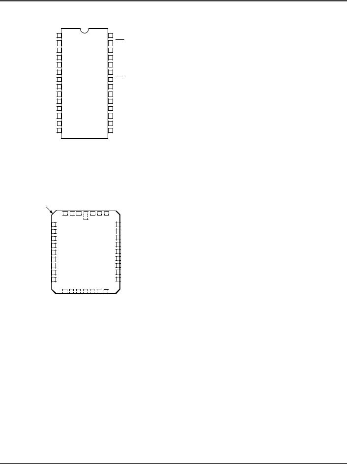
PIN CONFIGURATIONS
A14 |
1 |
|
28 |
V CC |
|
A12 |
2 |
|
27 |
WE |
|
A7 |
3 |
|
26 |
A13 |
|
A6 |
4 |
|
25 |
A8 |
|
A5 |
5 |
D28-3 |
24 |
A9 |
|
A4 |
6 |
23 |
A11 |
||
A3 |
7 |
P28-1 |
22 |
OE |
|
P28-2 |
|||||
A2 |
8 |
21 |
A10 |
||
D28-1 |
|||||
A1 |
9 |
20 |
CS |
||
SO28-5 |
|||||
A0 |
10 |
|
19 |
I/O 7 |
|
I/O 0 |
11 |
|
18 |
I/O 6 |
|
I/O 1 |
12 |
|
17 |
I/O 5 |
|
I/O 2 |
13 |
|
16 |
I/O 4 |
|
GND |
14 |
|
15 |
I/O 3 |
|
|
|
|
2946 drw 02 |
||
DIP/SOJ
TOP VIEW
|
|
A7 |
A12 |
14A |
NC VCC WE |
A |
|
|
INDEX |
|
|
|
|
13 |
|
||
|
|
|
|
|
|
|
||
|
|
|
|
|
|
|
||
|
|
|
|
|
|
|
|
|
|
|
4 |
3 |
2 |
32 31 30 |
|
||
A6 |
5 |
|
|
1 |
29 |
A8 |
||
|
|
|
||||||
A5 |
6 |
|
|
|
28 |
A9 |
||
A4 |
7 |
|
|
|
27 |
A11 |
||
A3 |
8 |
|
L32-1 |
26 |
NC |
|||
A2 |
9 |
|
25 |
OE |
||||
|
|
|
||||||
A1 |
10 |
|
|
|
24 |
A10 |
||
A0 |
11 |
|
|
|
23 |
CS |
||
NC |
|
12 |
|
|
|
22 |
I/O7 |
|
|
|
|
|
|||||
|
|
|
|
|||||
I/O0 |
|
13 |
|
|
|
21 |
I/O6 |
|
|
|
|
|
|||||
|
|
|
|
|||||
|
|
14 15 16 |
17 18 19 20 |
|
|
|||
|
|
I/O1 |
I/O2 |
GND |
NC I/O3 I/O4 |
I/O5 |
2946 drw 03 |
|
32-Pin LCC
TOP VIEW
PIN DESCRIPTIONS
Name |
Description |
|
|
A0–A14 |
Addresses |
|
|
I/O0–I/O7 |
Data Input/Output |
|
|
CS |
Chip Select |
|
|
WE |
Write Enable |
|
|
OE |
Output Enable |
|
|
GND |
Ground |
|
|
VCC |
Power |
|
|
2946 tbl 01
TRUTH TABLE(1)
WE |
CS |
OE |
I/O |
Function |
|
|
|
|
|
X |
H |
X |
High-Z |
Standby (ISB) |
|
|
|
|
|
X |
VHC |
X |
High-Z |
Standby (ISB1) |
|
|
|
|
|
H |
L |
H |
High-Z |
Output Disabled |
|
|
|
|
|
H |
L |
L |
DOUT |
Read Data |
|
|
|
|
|
L |
L |
X |
DIN |
Write Data |
NOTE: |
|
|
|
2946 tbl 02 |
1. H = VIH, L = VIL, X = Don’t Care
ABSOLUTE MAXIMUM RATINGS(1)
Symbol |
Rating |
Com’l. |
Mil. |
|
Unit |
|
|
|
|
|
|
VTERM |
Terminal Voltage |
–0.5 to +7.0 |
–0.5 to +7.0 |
|
V |
|
with Respect |
|
|
|
|
|
to GND |
|
|
|
|
|
|
|
|
|
|
TA |
Operating |
0 to +70 |
–55 to +125 |
|
°C |
|
Temperature |
|
|
|
|
|
|
|
|
|
|
TBIAS |
Temperature |
–55 to +125 |
–65 to +135 |
|
°C |
|
Under Bias |
|
|
|
|
|
|
|
|
|
|
TSTG |
Storage |
–55 to +125 |
–65 to +150 |
|
°C |
|
Temperature |
|
|
|
|
|
|
|
|
|
|
PT |
Power Dissipation |
1.0 |
1.0 |
|
W |
|
|
|
|
|
|
IOUT |
DC Output |
50 |
50 |
|
mA |
|
Current |
|
|
|
|
NOTE: |
|
|
|
2946 tbl 03 |
|
1.Stresses greater than those listed under ABSOLUTE MAXIMUM RATINGS may cause permanent damage to the device. This is a stress rating only and functional operation of the device at these or any other conditions above those indicated in the operational sections of this specification is not implied. Exposure to absolute maximum rating conditions for extended periods may affect reliability.
CAPACITANCE (TA = +25°C, f = 1.0MHz)
Symbol |
Parameter(1) |
Conditions |
Max. |
|
Unit |
CIN |
Input Capacitance |
VIN = 0V |
11 |
|
pF |
|
|
|
|
|
|
CI/O |
I/O Capacitance |
VOUT = 0V |
11 |
|
pF |
|
|
|
|
|
|
NOTE: |
|
|
|
2946 tbl 04 |
|
1.This parameter is determined by device characterization, but is not production tested.
7.2 |
2 |

IDT71256S/L |
|
CMOS STATIC RAM 256K (32K x 8-BIT) |
MILITARY AND COMMERCIAL TEMPERATURE RANGES |
RECOMMENDED OPERATING TEMPERATURE AND SUPPLY VOLTAGE
Grade |
Temperature |
GND |
VCC |
|
|
|
|
Military |
–55°C to +125°C |
0V |
5.0V ± 10% |
|
|
|
|
Commercial |
0°C to +70°C |
0V |
5.0V ± 10% |
|
|
|
|
2946 tbl 05
RECOMMENDED DC OPERATING
CONDITIONS
Symbol |
Parameter |
Min. |
Typ. |
Max. |
Unit |
|
|
|
|
|
|
VCC |
Supply Voltage |
4.5 |
5.0 |
5.5 |
V |
|
|
|
|
|
|
GND |
Supply Voltage |
0 |
0 |
0 |
V |
|
|
|
|
|
|
VIH |
Input High Voltage |
2.2 |
— |
6.0 |
V |
|
|
|
|
|
|
VIL |
Input Low Voltage |
–0.5(1) |
— |
0.8 |
V |
NOTE: |
|
|
|
2946 tbl 06 |
|
1. VIL (min.) = –3.0V for pulse width less than 20ns, once per cycle.
DC ELECTRICAL CHARACTERISTICS(1, 2)
(VCC = 5.0V ± 10%, VLC = 0.2V, VHC = VCC - 0.2V)
|
|
|
|
|
|
71256S/L20 |
|
71256S/L25 |
|
|
71256S/L30 |
|
|
71256S/L35 |
|
|
|||||||||||||||
Symbol |
Parameter |
|
|
Power |
Com’l. |
|
Mil. |
|
Com’l. |
|
Mil. |
|
Com’l. |
|
Mil. |
|
Com’l. |
Mil. |
|
Unit |
|||||||||||
|
|
|
|
|
|
|
|
|
|
|
|
|
|
|
|
|
|
|
|
|
|
|
|
|
|
|
|
|
|
|
|
ICC |
Dynamic Operating Current |
|
|
S |
|
— |
|
|
— |
|
|
— |
|
150 |
|
|
|
— |
|
145 |
|
|
— |
140 |
|
mA |
|||||
|
CS £ VIL, Outputs Open |
|
|
|
|
|
|
|
|
|
|
|
|
|
|
|
|
|
|
|
|
|
|
|
|
|
|
|
|
|
|
|
|
|
|
|
|
|
|
|
|
|
|
|
|
|
|
|
|
|
|
|
|
|
|
|
|
|
|
|
|
|
|
|
VCC = Max., f = fMAX(2) |
|
|
L |
|
135 |
|
|
— |
|
|
115 |
|
130 |
|
|
|
— |
|
125 |
|
105 |
120 |
|
|
||||||
ISB |
Standby Power Supply |
|
|
S |
|
— |
|
|
— |
|
|
— |
|
20 |
|
|
|
— |
|
20 |
|
|
— |
20 |
|
mA |
|||||
|
Current (TTL Level) |
|
|
|
|
|
|
|
|
|
|
|
|
|
|
|
|
|
|
|
|
|
|
|
|
|
|
|
|
|
|
|
|
|
|
|
|
|
|
|
|
|
|
|
|
|
|
|
|
|
|
|
|
|
|
|
|
|
|
|
|
|
|
|
CS ³ VIH, VCC = Max., |
|
|
L |
|
3 |
|
|
— |
|
|
3 |
|
3 |
|
|
|
— |
|
3 |
|
3 |
3 |
|
|
||||||
|
Outputs Open, f = fMAX(2) |
|
|
|
|
|
|
|
|
|
|
|
|
|
|
|
|
|
|
|
|
|
|
|
|
|
|
|
|
|
|
ISB1 |
Full Standby Power Supply |
|
|
S |
|
— |
|
|
— |
|
|
— |
|
20 |
|
|
|
— |
|
20 |
|
|
— |
20 |
|
mA |
|||||
|
Current (CMOS Level) |
|
|
|
|
|
|
|
|
|
|
|
|
|
|
|
|
|
|
|
|
|
|
|
|
|
|
|
|
|
|
|
|
|
|
|
|
|
|
|
|
|
|
|
|
|
|
|
|
|
|
|
|
|
|
|
|
|
|
|
|
|
|
|
CS ³ VHC, VCC = Max., f = 0 |
|
|
L |
|
0.4 |
|
|
— |
|
|
0.4 |
|
1.5 |
|
|
|
— |
|
1.5 |
|
0.4 |
1.5 |
|
|
||||||
|
|
|
|
|
|
|
|
|
|
|
|
|
|
|
|
|
|
||||||||||||||
|
|
|
71256S/L45 |
|
71256S/L55 |
|
71256S/L70 |
|
71256S/L85(3) |
|
71256S/L100(3) |
|
|||||||||||||||||||
|
|
|
|
|
|
|
|
|
|
|
|
|
|
|
|
|
|
||||||||||||||
Symbol |
Parameter |
Power |
Com’l. |
Mil. |
Com’l. |
Mil. |
|
Com’l. |
|
Mil. |
|
Com’l. |
Mil. |
|
Com'l. |
Mil. |
|
Unit |
|||||||||||||
|
|
|
|
|
|
|
|
|
|
|
|
|
|
|
|
|
|
|
|
|
|
|
|
||||||||
ICC |
Dynamic Operating Current |
S |
|
— |
135 |
|
— |
|
135 |
|
— |
|
135 |
|
— |
|
135 |
|
|
— |
135 |
|
mA |
||||||||
|
CS £ VIL, Outputs Open |
|
|
|
|
|
|
|
|
|
|
|
|
|
|
|
|
|
|
|
|
|
|
|
|
|
|
|
|
|
|
|
|
|
|
|
|
|
|
|
|
|
|
|
|
|
|
|
|
|
|
|
|
|
|
|
|
|
|
|
|
|
|
|
VCC = Max., f = fMAX(2) |
L |
100 |
115 |
|
— |
|
115 |
|
— |
|
115 |
|
— |
|
115 |
|
|
— |
115 |
|
|
|||||||||
ISB |
Standby Power Supply |
S |
|
— |
20 |
|
— |
|
|
20 |
|
— |
|
|
20 |
|
— |
|
20 |
|
|
— |
20 |
|
mA |
||||||
|
Current (TTL Level) |
|
|
|
|
|
|
|
|
|
|
|
|
|
|
|
|
|
|
|
|
|
|
|
|
|
|
|
|
|
|
|
CS ³ VIH, VCC = Max., |
L |
3 |
3 |
|
— |
|
|
3 |
|
— |
|
|
3 |
|
— |
|
3 |
|
|
— |
3 |
|
|
|||||||
|
Outputs Open, f = fMAX(2) |
|
|
|
|
|
|
|
|
|
|
|
|
|
|
|
|
|
|
|
|
|
|
|
|
|
|
|
|
|
|
ISB1 |
Full Standby Power Supply |
S |
|
— |
20 |
|
— |
|
|
20 |
|
— |
|
|
20 |
|
— |
|
20 |
|
|
— |
20 |
|
mA |
||||||
|
Current (CMOS Level) |
|
|
|
|
|
|
|
|
|
|
|
|
|
|
|
|
|
|
|
|
|
|
|
|
|
|
|
|
|
|
|
|
|
|
|
|
|
|
|
|
|
|
|
|
|
|
|
|
|
|
|
|
|
|
|
|
|
|
|
|
|
|
|
CS ³ VHC, VCC = Max., f = 0 |
L |
0.4 |
1.5 |
|
— |
|
|
1.5 |
|
— |
|
|
1.5 |
|
— |
|
1.5 |
|
|
— |
1.5 |
|
|
|||||||
|
|
|
|
|
|
|
|
|
|
|
|
|
|
|
|
|
|
|
|
|
|
|
|
|
|
|
|
|
|
|
|
NOTES: |
|
|
|
|
|
|
|
|
|
|
|
|
|
|
|
|
|
|
|
|
|
|
|
|
|
|
|
|
|
2946 tbl 07 |
|
1.All values are maximum guaranteed values.
2.fMAX = 1/tRC, all address inputs cycling at fMAX; f = 0 means no address pins are cycling.
3.Also available: 120 and 150 ns military devices.
7.2 |
3 |
 Loading...